In the absence of confirmation by device specification sheets, SHARP takes no responsibility for any defects that may occur in equipment using any SHARP devices shown in
catalogs, data books, etc. Contact SHARP in order to obtain the latest device specification sheets before using any SHARP device.
1
DESCRIPTION
The LH168R is a 384-output TFT-LCD source
driver IC which can simultaneously display 16.7
million colors in 256 gray scales.
FEATURES
∑ Number of LCD drive outputs : 384
∑ Built-in 8-bit digital input DAC
∑ Dot-inversion drive : Outputs the inverted gray
scale voltages between LCD drive pins next to
each other
∑ 2-port input for each circuit of data inputs R, G
and B, and it is possible to sample and hold
display data of two pixels at the same time
∑ Possible to display 16.7 million colors in 256 gray
scales with reference voltage input of 18 gray
scales : This reference voltage input corresponds
to < correction and intermediate reference voltage
input can be abbreviated
∑ Cascade connection
∑ Sampling sequence :
Output shift direction can be selected
XO
1
, YO
1
, ZO
1
/XO
128
, YO
128
, ZO
128
or
ZO
128
, YO
128
, XO
128
/ZO
1
, YO
1
, XO
1
∑ Shift clock frequency : 65 MHz (MAX.)
∑ Supply voltages
≠ V
CC
(for logic system) : +2.5 to +3.6 V
≠ V
LS
(for LCD drive) : +13 V (MAX.)
∑ Package : 464-pin TCP (Tape Carrier Package)
PIN CONNECTIONS
LH168R
LH168R
384-output TFT-LCD Source Driver IC
XO
128
YO
128
ZO
128
382
383
384
XO
1
YO
1
ZO
1
1
2
3
CHIP SURFACE
GND
V
LS
GND
XB
7
XB
0
XA
7
XA
0
YA
7
YA
0
SPOI
VH
0
VH
32
VH
64
VH
96
VH
128
VH
160
VH
192
VH
224
VH
256
VL
256
VL
224
VL
192
VL
160
VL
128
VL
96
VL
64
VL
32
VL
0
POLB
POLA
CK
SPIO
LS
REV
YB
7
YB
0
ZB
7
ZB
0
ZA
7
ZA
0
LBR
V
CC
V
LS
GND
464
463
462
461
454
453
446
445
438
437
436
435
434
433
432
431
430
429
428
427
426
425
424
423
422
421
420
419
418
417
416
415
414
413
412
405
404
397
396
389
388
387
386
385
464-PIN TCP
TOP VIEW
NOTE :
Doesn't prescribe TCP outline.
LH168R
2
PIN NO.
SYMBOL
I/O
DESCRIPTION
1 to 384
XO
1
-ZO
128
O
LCD drive output pins
385, 462, 464
GND
≠
Ground pins
386
V
LS
≠
Power supply pin for analog circuit
387
V
CC
≠
Power supply pin for digital circuit
388
LBR
I
Shift direction selection input pin
389 to 396
ZA
0
-ZA
7
I
Data input pins
397 to 404
ZB
0
-ZB
7
I
Data input pins
405 to 412
YB
0
-YB
7
I
Data input pins
413
REV
I
LCD drive output polarity exchange input pin
414
LS
I
Latch input pin
415
SPIO
I/O
Start pulse input/cascade output pin
416
CK
I
Shift clock input pin
417, 418
POLA, POLB
I
Input data polarity exchange input pins
419 to 427
VL
0
-VL
256
I
Reference voltage input pins
428 to 436
VH
256
-VH
0
I
Reference voltage input pins
Data input pins
I
XB
0
-XB
7
454 to 461
Data input pins
I
XA
0
-XA
7
446 to 453
Data input pins
I
YA
0
-YA
7
438 to 445
Start pulse input/cascade output pin
I/O
SPOI
437
463
V
LS
≠
Power supply pin for analog circuit
PIN DESCRIPTION
LH168R
4
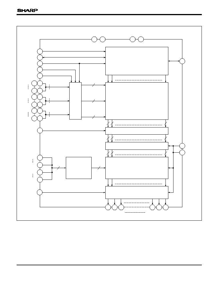
BLOCK
FUNCTION
Shift Register
Used as a bi-directional shift register which performs the shifting operation by CK and
selects bits for data sampling.
Data Latch
Used to temporary latch the input data which is sent to the sampling memory.
Sampling Memory
Used to sample the data to be entered by time sharing.
Hold memory
Used for latch processing of data in the sampling memory by LS input.
Level Shifter
Used to shift the data in the hold memory to the power supply level of the analog circuit
unit and sends the shifted data to DA converter.
Reference Voltage
Generation Circuit
Used to generate a gamma-corrected 256 x 2-level voltage by the resistor dividing circuit.
DA Converter
Used to generate an analog signal according to the display data and sends the signal to
the output circuit.
Output Circuit
Used as a voltage follower, configured with an operational amplifier and an output buffer,
which outputs analog signals of 256 x 2 gray scales to LCD drive output pin.
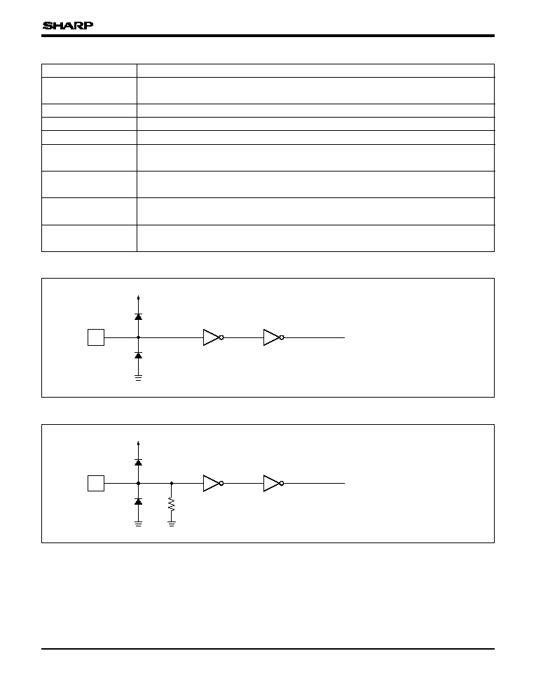
INPUT/OUTPUT CIRCUITS
I
V
CC
GND
To Internal Circuit
Fig. 1 Input Circuit (1)
øApplicable pins°
CK, LS, REV, LBR,
XA
0
-XA
7
, XB
0
-XB
7
,
YA
0
-YA
7
, YB
0
-YB
7
,
ZA
0
-ZA
7
, ZB
0
-ZB
7
I
V
CC
GND
GND
To Internal Circuit
Fig. 2 Input Circuit (2)
øApplicable pins°
POLA, POLB
FUNCTIONAL OPERATIONS OF EACH BLOCK