 | –≠–ª–µ–∫—Ç—Ä–æ–Ω–Ω—ã–π –∫–æ–º–ø–æ–Ω–µ–Ω—Ç: LH1694 | –°–∫–∞—á–∞—Ç—å:  PDF PDF  ZIP ZIP |
Document Outline
- ˛ˇ
- ˛ˇ
- ˛ˇ
- ˛ˇ
- ˛ˇ
- ˛ˇ
- ˛ˇ
- ˛ˇ
- ˛ˇ
- ˛ˇ
- ˛ˇ
- ˛ˇ
- ˛ˇ
In the absence of confirmation by device specification sheets, SHARP takes no responsibility for any defects that may occur in equipment using any SHARP devices shown in
catalogs, data books, etc. Contact SHARP in order to obtain the latest device specification sheets before using any SHARP device.
1
DESCRIPTION
The LH1694 is a 256-output TFT-LCD gate driver
IC.
FEATURES
∑ Number of LCD drive outputs : 256
∑ LCD drive output sequence :
Output shift direction can be selected
OG
1
/OG
256
or OG
256
/OG
1
∑ Enable chain connection
∑ Usable with both positive/negative power supplies
∑ Output signal masking function
∑ Input signal voltage : +2.7 to +3.6 V
∑ LCD drive voltage : +16.0 to +42.0 V
∑ Operating temperature : ≠30 to +85 ∞C
∑ Package : 277-pin TCP (Tape Carrier Package)
PIN CONNECTIONS
LH1694
LH1694
256-output TFT-LCD Gate Driver IC
OG
254
OG
255
OG
256
254
255
256
OG
1
OG
2
OG
3
1
2
3
CHIP SURFACE
V
DD
V
EE
V
SS
V
CC
V
LS
GND
SVIO
R/L
CKV
OE
1
OE
2
OE
3
SVOI
GND
TEST
2
TEST
1
V
LS
V
CC
V
SS
V
EE
V
DD
277
276
275
274
273
272
271
270
269
268
267
266
265
264
263
262
261
260
259
258
257
277-PIN TCP
TOP VIEW
NOTE :
Doesn't prescribe TCP outline.
2
LH1694
PIN DESCRIPTION
BLOCK DIAGRAM
PIN NO.
SYMBOL
I/O
DESCRIPTION
1 to 256
OG
1
-OG
256
O
LCD drive output pins
257, 277
V
DD
≠
Power supply pins for LCD drive
258, 276
V
EE
≠
Power supply pins for LCD drive
259, 275
V
SS
≠
Power supply pins for logic system
260, 274
V
CC
≠
Power supply pins for logic system
261, 273
V
LS
≠
Power supply pins for logic input/output systems
265
SVOI
I/O
Vertical scanning start pulse input/output pin
266 to 268
OE
3
-OE
1
I
Input pins for output enable
269
CKV
I
Vertical shift clock input pin
270
R/L
I
Pin for selecting bi-directional shift register and setting cascade sequence
257
V
DD
262
263
TEST
1
TEST
2
SVOI
OE
3
OE
2
OE
1
CKV
R/L
SVIO
265
266
267
268
269
270
271
V
DD
277
261
V
LS
V
LS
273
264
GND GND
272
260
V
CC
V
CC
274
258
V
EE
V
EE
276
259
V
SS
V
SS
275
OG
1
1
OG
256
256
OUTPUT CIRCUIT
LEVEL SHIFTER
BI-DIRECTIONAL SHIFT
REGISTER
CONTROL
LOGIC
1
256
1
256
1
256
IC test pins
I
TEST
1
, TEST
2
262, 263
Ground pins for logic input
≠
GND
264, 272
Vertical scanning start pulse input/output pin
I/O
SVIO
271
3
LH1694
FUNCTIONAL OPERATIONS OF EACH BLOCK
BLOCK
FUNCTION
Control Logic
Used to create signals necessary for mode selecting signal, cascade sequence setting
signal and for operation of bi-directional shift register.
Bi-directional Shift
Register
Used as transfer circuit of LCD drive output start signal. It is possible to set LCD drive
output sequence of OG
1
/
OG
256
direction or OG
256
/
OG
1
direction.
Level Shifter
Used as circuit which shifts LCD drive output signals transferred by bi-directional shift
register to V
DD
-V
EE
level.
Output Circuit
Configured with output buffers to output V
DD
-V
EE
level.
INPUT/OUTPUT CIRCUITS
I
V
LS
Level Shifter
(V
LS
-GND
/
V
CC
-V
SS
)
Internal Logic
(V
CC
-V
SS
)
V
SS
To Internal Circuit
,
Fig. 1 Input Circuit
øApplicable pins°
CKV, R/L, OE
1
-OE
3
,
TEST
1
, TEST
2
V
LS
V
SS
(V
LS
-GND)
Output Signal
Output Control Signal
V
LS
Level Shifter
(V
LS
-GND
/
V
CC
-V
SS
)
V
SS
To Internal
Circuit
I
O
Fig. 2 Input/Output Circuit
øApplicable pins°
SVIO, SVOI
4
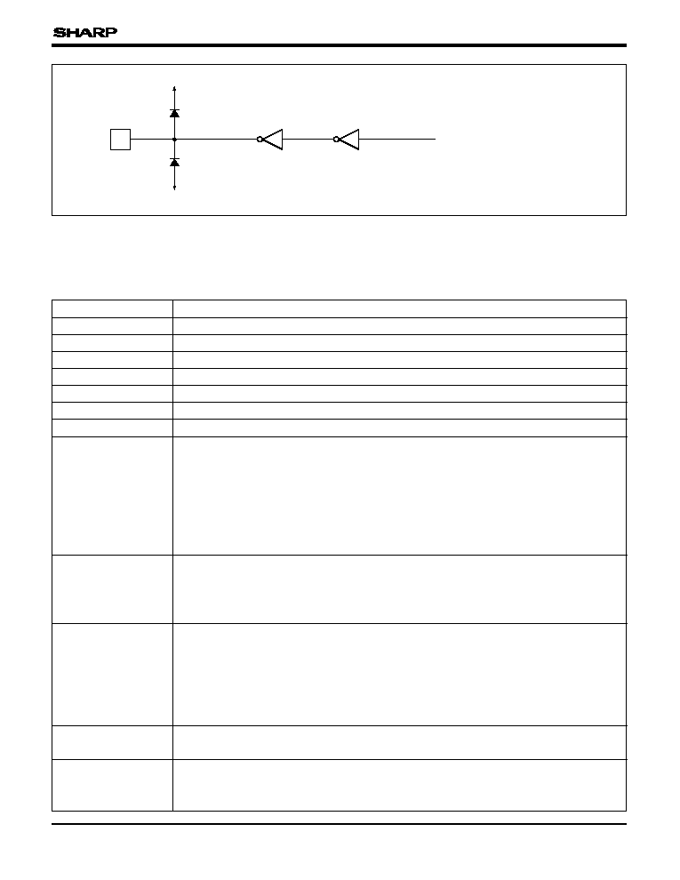
LH1694
O
V
DD
(V
DD
-V
EE
)
V
EE
From Internal Circuit
Fig. 3 Output Circuit
øApplicable pins°
OG
1
-OG
256
FUNCTIONAL DESCRIPTION
Pin Functions
SYMBOL
FUNCTION
V
DD
Used as power supply pin for high level LCD drive.
V
LS
Used as power supply pin for input level shifters.
V
CC
Used as power supply pin for logic system, normally connected to V
SS
+ 5.0 V.
V
EE
Used as power supply pin for low level LCD drive.
V
SS
Used as logic system power supply pin.
CKV
Used as vertical shift clock pulse input pin.
SVIO
SVOI
Used as vertical scanning start pulse input/output pins.
Data input/output pins for shift register. During input, data is read at the rising edge of the
CKV. During output, data is output at the falling edge of the CKV.
∑ When R/L = "H".
SVOI is set to data output pin for next cascade, and SVIO is set to input pin for shift data.
∑ When R/L = "L".
SVOI is set to input pin for shift data, and SVIO is set to data output pin for next cascade.
R/L
Used as input pin for selecting the shift direction of bi-directional shift register and for
setting the sequence of cascade connection.
LCD drive outputs shift from OG
1
to OG
256
when set to "H". LCD drive outputs shift from
OG
256
to OG
1
when set to "L".
OE
1
OE
2
OE
3
Input pins for output-enable. LCD drive output is set to "L", when OE
1
, OE
2
, and OE
3
pins
are set to "H", and it has no relation with clock input.
Relationship between enable control and output pins;
OE
1
: OG
1
, OG
4
OG
250
, OG
253
, OG
256
OE
2
: OG
2
, OG
5
OG
251
, OG
254
OE
3
: OG
3
, OG
6
OG
252
, OG
255
TEST
1
TEST
2
Used as input pins for IC testing.
Must be set to "H".
OG
1
-OG
256
Used as output pins for LCD drive output, and which output data at 2 levels.
∑ Selecting data is output at V
DD
level .
∑ Non-selecting data is output at V
EE
level .
Used as power supply pin for input level shifters.
GND
5
LH1694
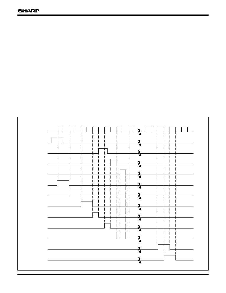
Example of Input/Output Timing (R/L = "H")
1
2
3
4
5
6
7
255
256
257
258
CKV
SVIO
(Input)
OE
1
OE
2
OE
3
OG
1
OG
2
OG
3
OG
4
OG
5
OG
6
OG
256
SVIO
(Output)
∑
∑
∑
∑
∑
Functional Operations
LH1694 can select the LCD drive output level (OG
1
to OG
256
) by the set of the input signal (CKV,
SVIO, SVOI, OE
1
, OE
2
, OE
3
).
When the pin for selecting the bi-directional shift
register (R/L) is set to "H", LCD drive outputs shift
from OG
1
to OG
256
, and when set to "L", LCD
drive outputs shift from OG
256
to OG
1
.
OE
1
,OE
2
and OE
3
are signals for output-enable.
Output pins output non-selecting data (V
EE
level)
when OE
1
to OE
3
pins are set to "H" and it has no
relation with input clock.
While R/L = "H" input data from SVIO is read at the
rising edge of shift clock (CKV), and outputs to
LCD drive output pin OG
1
at the width for one
cycle of shift clock. Next LCD drive output pins from
OG
2
to OG
256
are sequentially shifted at the rising
edge of the CKV for one cycle. Shift signal of
OG
256
is read at the falling edge of the clock
signal, and the input data for the next cascade is
output from the SVOI pin.
While R/L = "L" input data from SVOI is read at the
rising edge of shift clock (CKV), and outputs to LCD
drive output pin OG
256
at the width for one cycle of
shift clock. Next LCD drive output pins from OG
255
to
OG
1
are sequentially shifted at the rising edge of the
CKV for one cycle. Shift signal of OG
1
is read at the
falling edge of the clock signal and the input data for
the next cascade is output from the SVIO pin.