Data Sheet
1
LH28F016SCT
Data Sheet
16M Flash Memory
FEATURES
∑ SmartVoltage Technology
≠ 2.7 V (Read Only), 3.3 V or 5 V V
CC
≠ 3.3 V, 5 V, or 12 V V
PP
∑ High Performance Read Access Time
≠ 95 ns (5 V ±0.25 V)
≠ 100 ns (5 V ±0.5 V)
≠ 120 ns (3.3 V ±0.3 V)
≠ 150 ns (2.7 V - 3.6 V)
∑ High Density Symmetrically-Blocked Architecture
≠ Thirty-two 64KB Erasable Blocks
∑ Low Power Management
≠ Deep Power Down Mode
≠ Automatic Power Savings Mode Decreases I
CC
in Static Mode
∑ Enhanced Data Protection Features
≠ Absolute Protection with V
PP
= GND
≠ Flexible Block Locking
≠ Block Erase/Byte Write Lockout during Power
Transitions
∑ Automated Byte Write and Block Erase
≠ Command User Interface
≠ Status Register
∑ Enhanced Automated Suspend Options
≠ Byte Write Suspend to Read
≠ Block Erase Suspend to Byte Write
≠ Block Erase Suspend to Read
∑ Extended Cycling Capability
≠ 100,000 Block Erase Cycles
≠ 3.2 Million Block Erase Cycles/Chip
∑ SRAM Compatible Write Interface
∑ Industry Standard Packaging
≠ 40-Lead TSOP
∑ Operating Temperature
≠ 0∞C to +70∞C
∑ ETOXTM Nonvolatile Flash Technology
∑ CMOS Process (P-type Silicon Substrate)
∑ Not Designed or Rated as Radiation Hardened
DESCRIPTION
SHARP's LH28F016SCT Flash memory with Smart-
Voltage technology is a high density, low cost, nonvol-
atile, read/write storage solution for a wide range of
applications. Its symmetrically blocked architecture,
flexible voltage, and extended cycling provide for
highly flexible component suitable for resident flash
arrays, SIMMs and memory cards. Its enhanced sus-
pend capabilities provide for an ideal solution for code
and data storage applications. For secure code stor-
age applications, such as networking, where code is
either directly executed out of flash or downloaded to
DRAM, the LH28F016SCT offers three levels of pro-
tection: absolute protection with V
PP
at GND, selective
hardware block locking, or flexible software block lock-
ing. These alternatives give designers ultimate control
of their code security needs.
The LH28F016SCT is manufactured on SHARP's
0.38
µ
m ETOXTM V process technology. Available in
the industry-standard package of 40-lead TSOP, it is
i d e al fo r bo a r d- c o n s t ra i n e d a pp l i c a ti o n s . T he
LH28F0016SCT is based on the 28F008SA architec-
ture, and is a quick and easy upgrade for designs
demanding the state-of-the-art.
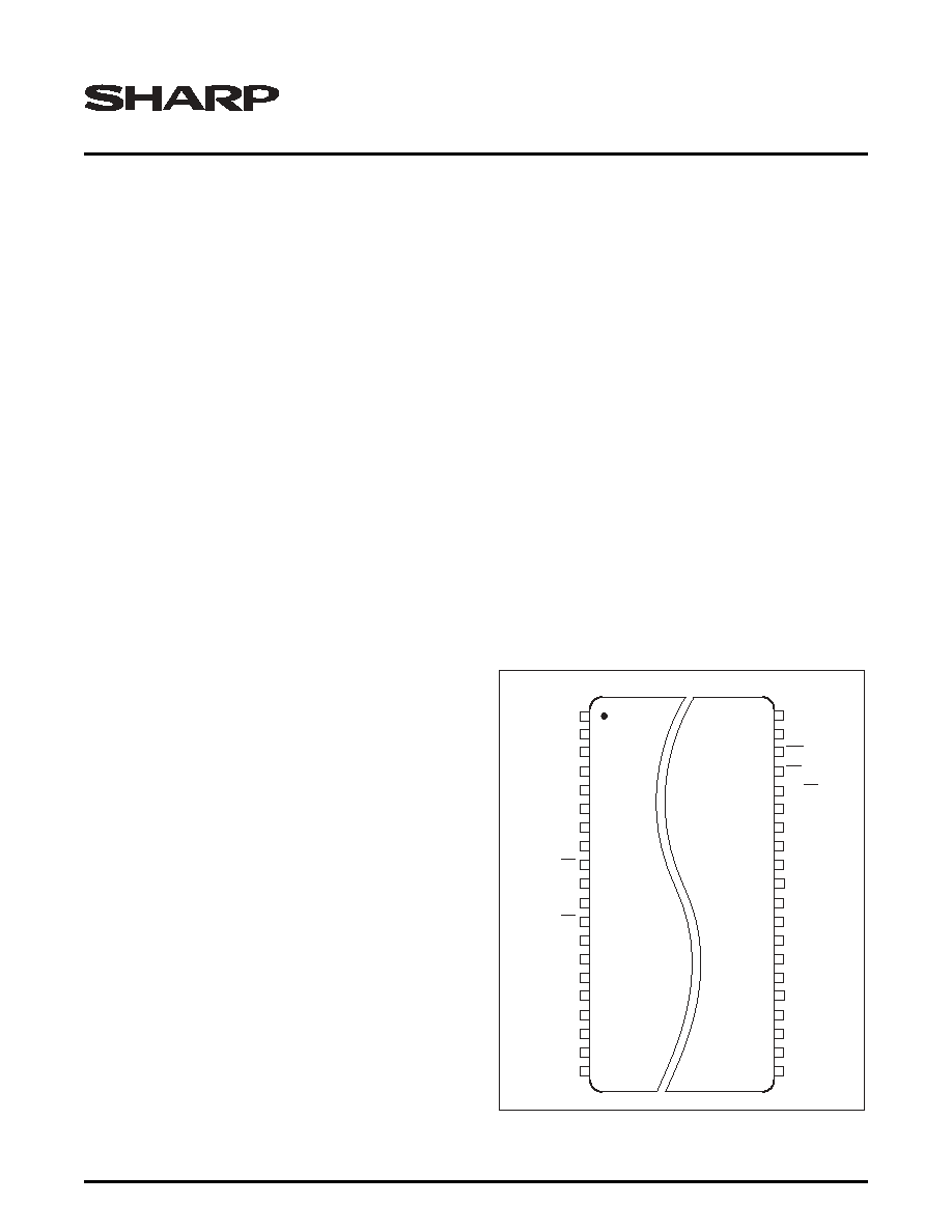
Figure 1. LH28F016SCT Pinout
28F016SCT-L95-1
TOP VIEW
40-PIN TSOP
2
3
4
5
8
9
A
12
A
15
37
36
35
34
33
32
29
26
6
7
A
13
A
14
A
16
A
19
A
17
A
18
31
30
OE
DQ
6
10
11
12
39
38
WE
13
28
DQ
3
DQ
2
DQ
1
27
DQ
7
RY/BY
A
20
14
15
16
17
18
19
20
23
25
24
22
21
A
0
A
1
A
2
A
3
A
6
A
5
A
7
A
4
A
10
A
9
A
11
A
8
NC
DQ
5
DQ
4
V
CC
GND
DQ
0
40
1
V
PP
V
CC
RP
CE
GND
* ETOX is a trademark of Intel Corporation.
LH28F016SCT
16M Flash Memory
2
Data Sheet
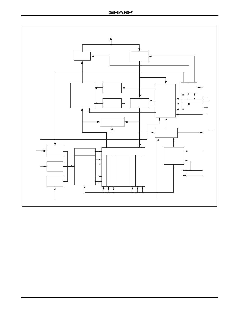
Figure 2. LH28F016SCT Block Diagram
OUTPUT
BUFFER
INPUT
BUFFER
DQ
7
-
DQ
0
IDENTIFIER
REGISTER
OUTPUT
MULTIPLEXER
STATUS
REGISTER
DATA
REGISTER
WRITE STATE
MACHINE
DATA
COMPARATOR
COMMAND
REGISTER
I/O
LOGIC
. . .
Y GATING
32
64KB
BLOCKS
Y-DECODER
X DECODER
WE
CE
OE
V
CC
RP
PROGRAM/
ERASE
VOLTAGE
SWITCH
V
PP
V
CC
GND
ADDRESS
COUNTER
ADDRESS
LATCH
INPUT
BUFFER
A
20
- A
0
. . .
28F016SCT-L95-2
RY/BY

16M Flash Memory
LH28F016SCT
Data Sheet
3
Table 1. Pin Descriptions
SYMBOL
TYPE
DESCRIPTION
A
20
- A
0
Input
Address Inputs
Inputs for addresses during read and write operations. Addresses are in-
ternally latched during a write cycle.
DQ
7
- DQ
0
Input/
Output
Data Input/Outputs
Inputs data and commands during CUI write cycles; outputs data dur-
ing memory array, status register, and identifier code read cycles. Data pins float to high-
impedance when the chip is deselected or outputs are disabled. Data is internally latched
during a write cycle.
CE
Input
Chip Enable
Activates the device's control logic, input buffers, decoders, and sense am-
plifiers. CE HIGH deselects the device and reduces power consumption to standby levels.
RP
Input
Reset/Deep Power-down
Puts the device in deep power-down mode and resets internal
automation. RP HIGH enables normal operation. When driven LOW, RP inhibits write oper-
ations which provides data protection during power transitions. Exiting from deep power-
down sets the device to read array mode. RP at V
HH
enables setting of the master lock-bit
and enables configuration of block lock-bits when the master lock-bit is set. RP = V
HH
over-
rides block lock-bits thereby enabling block erase and byte write operations to locked mem-
ory blocks. Block erase, byte write, or lock-bit configuration with V
IH
< RP < V
HH
produce
spurious results and should not be attempted.
OE
Input
Output Enable
Gates the device's outputs during a read cycle.
WE
Input
Write Enable
Controls writes to the CUI and array blocks. Addresses and data are latched
on the rising edge of the WE pulse.
RY/BY
Output
Read/Busy
Indicates the status of the internal WSM. When LOW, the WSM is performing
an internal operation (block erase, byte write, or lock-bit configuration). RY/BY HIGH indi-
cates that the WSM is ready for new commands, block erase is suspended, and byte write
is inactive, byte write is suspended, or the device is in deep power-down mode. RY/BY is
always active and does not float when the chip is deselected or data outputs are disabled.
V
PP
Supply
Block Erase, Byte Write, Lock Bit Configuration Power Supply
For erasing array
blocks, writing bytes, or configuring lock-bits. With V
PP
V
PPLK
, memory contents cannot be
altered. Block erase, byte write, and lock-bit configuration with an invalid V
PP
(see DC Char-
acteristics) produce spurious results and should not be attemped.
V
CC
Supply
Device Power Supply
Internal detection configures the device for 2.7 V, 3.3 V, or 5 V
operation. To switch from one voltage to another, ramp V
CC
down to GND and then ramp
V
CC
to the new voltage. Do not float any power pins. With V
CC
V
LKO
, all write attempts to
the flash memory are inhibited. Device operations at invalid V
CC
voltage (see `DC Charac-
teristics) produce spurious results and should not be attempted. Block erase, byte write and
lock-bit configuration operations with V
CC
< 3.0 V are not supported.
GND
Supply Ground
Do not float any ground pins.
NC
Non-connect
Lead is not internal connected; it may be driven or floated.

LH28F016SCT
16M Flash Memory
4
Data Sheet
OVERVIEW
The LH28F160SCT-L95 is a high-performance 16M
SmartVoltage Flash memory organized as 2MB ◊ 8
bits. The 2MB of data is arranged in thirty-two 64KB
blocks which are indivdually eraseable, lockable, and
unlockable in-system. The memory map is shown in
Figure 3.
SmartVoltage technology provides a choice of V
CC
and V
PP
combinations, as shown in Table 2, to meet
system performance and power expectations. 2.7 V
V
CC
consumes approximately one-fifth the power of
5 V V
CC
, V
PP
at 3.3 V, and 5 V eliminates the need for
a separate 12 V converter, while V
PP
= 12 V maximizes
block erase and byte write performance. In addition to
flexible erase and program voltages, the dedicated V
PP
pin gives complete data protection when V
PP
V
PPLK
.
NOTE: Block erase, byte write and lock-bit configuration operations
with V
CC
< 3 V are not supported.
Internal V
CC
and V
PP
detection cicuitry automati-
cally configures the device for optimized read and write
operations.
A Command User Interface (CUI) serves as the
interfaces between the system processor and internal
operation of the device. A valid command sequence
written to the CUI initiates device automation. An inter-
nal Write State Machine (WSM) automatically executes
the algorithms and timings necessary for block erase,
byte write, and lock-bit configuration operations.
A block erase operation erases one of the device's
64KB blocks typically within 1 second (5 V V
CC
,
12 V V
PP
) independent of other blocks. Each block can
be independently erased 100,000 times. (3.2 million
block erases per device). Block erase suspend mode
allows system software to suspend block erase to read
from or write data to any other block.
Writing memory data is performed in byte increments
typically within 6 µs (5 V V
CC
, 12 V V
PP
). Byte write sus-
pend mode enables the system to read data or execute
code from any other flash memory array location.
Individual block locking uses a combination of bits,
thirty-two block lock-bits and a master lock-bit, to lock
and unlock blocks. Block lock-bits gate block erase and
byte write operations, while the master lock-bit gates
block lock-bit modification. Lock-bit confifuration oper-
ations (Set Block Lock-Bit, Set Master Lock-Bit, and
Clear Block Lock-Bits commands) set and cleared
lock-bits.
The status register indicates when the WSM's block
erase, byte write, or lock-bit configuration operation is
finished.
Figure 3. Memory Map
15
1F0000
1FFFFF
1EFFFF
1E0000
1DFFFF
1D0000
1CFFFF
1C0000
1BFFFF
1B0000
1AFFFF
1A0000
19FFFF
190000
18FFFF
180000
17FFFF
170000
16FFFF
160000
15FFFF
150000
14FFFF
140000
13FFFF
130000
12FFFF
120000
11FFFF
110000
10FFFF
100000
0FFFFF
0F0000
0EFFFF
0E0000
0DFFFF
0D0000
0CFFFF
0C0000
0BFFFF
0B0000
0AFFFF
0A0000
09FFFF
090000
08FFFF
080000
07FFFF
070000
06FFFF
060000
05FFFF
050000
04FFFF
040000
03FFFF
030000
02FFFF
020000
01FFFF
010000
00FFFF
000000
14
13
12
11
10
9
8
7
6
5
4
3
2
0
64KB BLOCK
16
64KB BLOCK
17
64KB BLOCK
18
64KB BLOCK
19
64KB BLOCK
20
64KB BLOCK
21
64KB BLOCK
22
64KB BLOCK
23
64KB BLOCK
24
64KB BLOCK
25
64KB BLOCK
26
64KB BLOCK
27
64KB BLOCK
28
64KB BLOCK
29
64KB BLOCK
30
64KB BLOCK
31
64KB BLOCK
64KB BLOCK
64KB BLOCK
64KB BLOCK
64KB BLOCK
64KB BLOCK
64KB BLOCK
64KB BLOCK
64KB BLOCK
64KB BLOCK
64KB BLOCK
64KB BLOCK
64KB BLOCK
64KB BLOCK
1
64KB BLOCK
64KB BLOCK
28F016SCT-L95-3
Table 2. V
CC
and V
PP
Voltage Combinations
Offered by SmartVoltage Technology
V
CC
VOLTAGE
V
PP
VOLTAGE
2.7 V (See Note)
3.3 V
3.3 V, 5 V, 12 V
5 V
5 V, 12 V

16M Flash Memory
LH28F016SCT
Data Sheet
5
The RY/BY output gives an additional indicator of
WSM activity by providing both a hardware signal of
status (versus software polling) and status masking
(interrupt masking for background block erase, for
example). Status polling using RY/BY minimizes both
CPU overhead and system power consumption. When
LOW, RY/BY indicates that the WSM is performing a
block erase, byte write, or lock-bit configuration.
RY/BY HIGH indicates that the WSM is ready for a
new command, block erase is suspended (and byte
write is inactive), byte is suspended, (and byte write is
inactive), byte write is suspended, or the device is in
deep power-down mode.
The access time is 95 ns (t
AVQV
) over the commeri-
cal temperature range (0∞C to 70∞C) and V
CC
supply
voltage range of 4.75 V - 5.25 V. At lower V
CC
voltages,
the access times are 100 ns (4.5 V - 5.5 V), 120 ns
(3.0 V - 3.6 V) and 150 ns (2.7 V - 3.6 V).
The Automatic Power Savings (APS) feature sub-
stantially reduces active current when the device is in
static mode (address not switching). In APS mode, the
typical I
CCR
current is 1 mA at 5 V V
CC
.
When CE
and RP pins are at V
CC
, the I
CC
CMOS
standby mode is enabled. When the RP pin is at GND,
deep power-down mode is enabled which minimizes
power consumption and provides write protection dur-
ing Reset. A reset time (t
PHQV
) is required from RP
going HIGH until outputs are valid. Likewise, the device
has a wake time (t
PHEL
) from RP HIGH until writes to
the CUI are recognized. With RP at GND, the WSM is
reset and the status register is cleared. The device is
available in 40-pin TSOP packaging. Pinout is as shown
in Figure 1.
PRINCIPLES OF OPERATION
The LH28F016SCT SmartVoltage flash memory
includes an on-chip Write State Machine (WSM) to
manage block erase, byte write, and lock-bit configura-
tion functions. It allows for: 100% TTL-level control
inputs, fixed power supplies during block erasure, byte
write, and lock-bit configuration, and minimal process
overhead with RAM-like interface timings.
After initial device power-up or return from Reset
mode (see `Bus Operations' section), the device
defaults to read array mode. Manipulation of external
memory control pins allow array read, standby, and
output disable operations.
Status register and identifier codes can be accessed
through the Command User Interface (CUI), indepen-
dent of the V
PP
voltage. High voltage on V
PP
enables
successful block erase, byte writing, and lock-bit config-
uration. All functions associated with altering memory
contents-block erase, byte write, lock-bit configuration,
status, and identifier codes are accessed via the CUI
and verified through the status register.
Commands are written using standard microproces-
sor write timings. The CUI contents serve as input to
the WSM, which controls the block erase, byte write,
and lock-bit configuration. The internal algorithms are
regulated by the WSM, including pulse repetition, inter-
nal verification, and margining of data. Addresses and
data are internally latch during write cycles. Writing the
appropriate command outputs array data, accesses
the identifier codes, or outputs status register data.
Interface software that initiates and polls progress of
block erase, byte write, and lock-bit configuration can
be stored in any block. This code is copied to and exe-
cuted from system RAM during flash memory updates.
After successful completion, reads are again possible
via the Read Array command. Block erase suspend
allows system software to suspend a block erase to
read or write data from any other block. Byte write sus-
pend allows system software to suspend a byte write to
read data from any other flash memory array location.
Data Protection
Depending on the application, the system designer
may choose to make the V
PP
power supply switchable
(available only when memory block erase, byte writes,
or lock-bit configurations are required) or hardwired to
V
PPH1/2/3
. The device accommodates either design
practice and encourages optimaization of the proces-
sor-memory interface.
When V
PP
V
PPLK
, memory contents cannot be
altered. The CUI, with the two-step block erase, byte
write, or lock-bit configuration command sequences,
provides protection from unwanted operations even
when high voltage is applied to V
PP
. All write functions
are disabled when V
CC
is below the write lockout volt-
age V
LKO
or when RP is at V
IL
. The device's block lock-
ing capability provides additional protection from
inadvertent code or data alteration by gating block
erase, and byte write operations.
BUS OPERATION
The local CPU reads and writes the flash memory in-
system. All bus cycles to or from the flash memory con-
form to standard microprocessor bus cycles.