
1
LH28F020SU-N
2M (256K ◊ 8) Flash Memory
Figure 1. TSOP Configuration
28F020SUN80-1
TOP VIEW
32-PIN TSOP
2
3
4
5
8
9
A
14
29
28
27
26
25
24
21
18
6
7
A
17
A
13
A
11
A
8
A
9
23
22
DQ
4
10
11
12
31
30
CE
13
20
A
0
A
1
A
2
19
DQ
5
DQ
6
DQ
7
A
10
OE
14
15
16
17
A
15
A
16
A
12
A
7
A
6
A
5
A
4
DQ
3
DQ
1
DQ
2
DQ
0
GND
A
3
32
1
V
PP
V
CC
WE
Figure 2. SOP Configuration
28F020SUN80-20
TOP VIEW
32-PIN SOP
2
3
4
5
8
9
A
7
29
28
27
26
25
24
21
18
6
7
A
5
A
4
A
3
A
6
A
12
V
PP
A
15
A
16
23
22
A
9
10
11
12
31
30
13
20
DQ
6
DQ
7
DQ
5
DQ
4
19
A
8
A
13
A
17
A
14
V
CC
14
15
16
17
A
1
A
2
A
0
DQ
0
DQ
1
DQ
2
GND
WE
A
11
OE
A
10
CE
DQ
3
32
1
FEATURES
∑
256K ◊ 8 Bit Configuration
∑
5 V Write/Erase Operation (5 V V
PP
)
≠ No Requirement for DC/DC Converter to
Write Erase
∑
80 ns Maximum Access Time
∑
16 Independently Lockable Blocks (16K)
∑
100,000 Erase Cycles per Block
∑
Automated Byte Write/Block Erase
≠ Command User Interface
≠ Status Register
∑
System Performance Enhancement
≠ Erase Suspend for Read
≠ Two-Byte Write
≠ Full Chip Erase
∑
Data Protection
≠ Hardware Erase/Write Lockout during
Power Transitions
≠ Software Erase/Write Lockout
∑
Independently Lockable for Write/Erase on
Each Block (Lock Block and Protect
Set/Reset)
∑
5 µA (TYP.) I
CC
in CMOS Standby
∑
State-of-the-Art 0.55 µm ETOXTM Flash
Technology
∑
Packages
≠ 32-Pin, 525 mil. SOP Package
≠ 32-Pin, 1.2 mm ◊ 8 mm ◊ 20 mm
TSOP (Type I) Package
LH28F020SU-N
2M (256K ◊ 8) Flash Memory
2
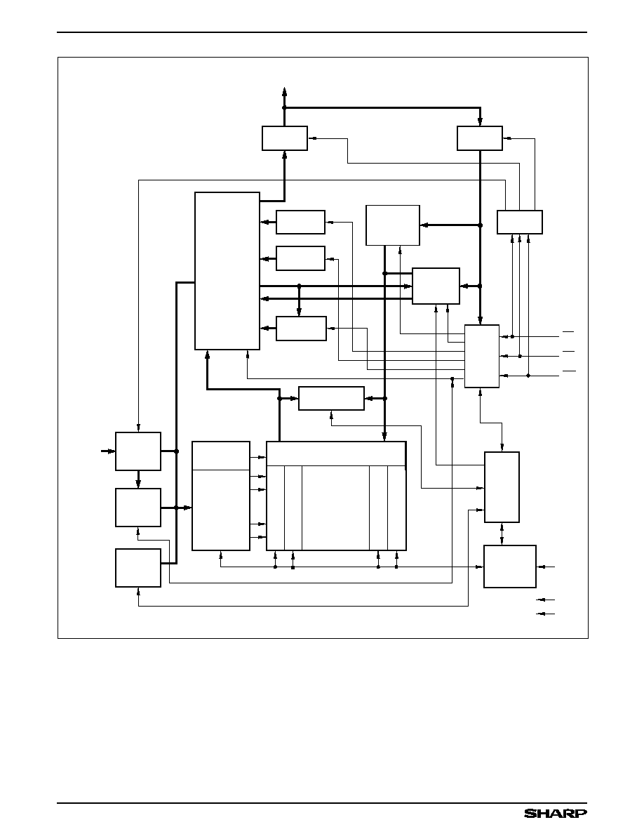
Figure 3. LH28F020SU-N Block Diagram
OUTPUT
BUFFER
INPUT
BUFFER
DQ
0
-
DQ
7
ID
REGISTER
OUTPUT
MULTIPLEXER
CSR
ESRs
DATA
COMPARATOR
DATA
QUEUE
REGISTER
REGISTER
I/O
LOGIC
CUI
WSM
16KB BLOCK 0
16KB BLOCK 1
16KB BLOCK 14
16KB BLOCK 15
. . .
. . .
Y GATING/SENSING
Y-DECODER
X-DECODER
OE
CE
WE
PROGRAM/
ERASE
VOLTAGE
SWITCH
V
PP
V
CC
GND
ADDRESS
COUNTER
ADDRESS
QUEUE
LATCH
INPUT
BUFFER
A
0
- A
17
. . .
28F020SUN80-2

2M (256K ◊ 8) Flash Memory
LH28F020SU-N
3
INTRODUCTION
Sharp's LH28F020SU-N 2M Flash Memory is a revo-
lutionary architecture which enables the design of truly
mobile, high performance, personal computing and com-
munication products. With innovative capabilities, 5.0 V
single voltage operations and very high read/write per-
formance, the LH28F020SU-N is also the ideal choice
for designing embedded mass storage flash memory
systems.
The LH28F020SU-N is a very high density, highest
performance non-volatile read/write solution for solid-
state storage applications. Its independently lockable
16 symmetrical blocked architecture (16K each)
extended cycling, low power operation, very fast write
and read performance and selective block locking pro-
vide a highly flexible memory component suitable for
high density memory cards, Resident Flash Arrays and
PCMCIA-ATA Flash Drives. The LH28F020SU-N single
voltage power supply operation enables the design of
memory cards which can be read/written in 5.0 V sys-
tems. Its x8 architecture allows the optimization of
memory to processor interface. The flexible block lock-
ing option enables bundling of executable application
software in a Resident Flash Array or memory card.
Manufactured on Sharp's 0.55 µm ETOXTM process
technology, the LH28F020SU-N is the most cost-
effective, high density 5.0 V flash memory.
Description
The LH28F020SU-N is a high performance 2M
(2,097,152 bit) block erasable non-volatile random
access memor y organized as 256K ◊ 8. The
LH28F020SU-N includes sixteen 16K (16,384) blocks.
A chip memory map is shown in Figure 4.
The implementation of a new architecture, with many
enhanced features, will improve the device operating
characteristics and results in greater product reliability
and ease of use.
Among the significant enhancements of the
LH28F020SU-N80:
∑
5 V Read, Write/Erase Operation
(5 V V
CC,
5.0 V V
PP
)
∑
Lower Power Capability
∑
Improved Write Performance
∑
Dedicated Block Write/Erase Protection
∑
Command-Controlled Memory Protection
Set/Reset Capability
The LH28F020SU-N will be available in a 32-pin,
525 mil. SOP package. This form factor and pinout al-
low for very high board layout densities.
PIN DESCRIPTION
SYMBOL
TYPE
NAME AND FUNCTION
A
0
- A
13
INPUT
BYTE-SELECT ADDRESSES
: Select a byte within one 16K block. These
addresses are latched during Data Writes.
A
14
- A
17
INPUT
BLOCK-SELECT ADDRESSES
: Select 1 of 16 Erase Blocks. These addresses are
latched during Data Writes, Erase and Lock-Block operations.
DQ
0
- DQ
7
INPUT/OUTPUT
DATA INPUT/OUTPUT:
Inputs data and commands during CUI write cycles.
Outputs array, buffer, identifier or status data in the appropriate Read mode.
Floated when the chip is de-selected or the outputs are disabled.
CE
ª
INPUT
CHIP ENABLE INPUTS
: Activate the device's control logic, input buffers, decoders
and sense amplifiers. CE
ª
must be low to select the device.
OE
ª
INPUT
OUTPUT ENABLE
: Gates device data through the output buffers when low. The
outputs float to tri-state off when OE
ª
is high.
WE
INPUT
WRITE ENABLE:
Controls access to the CUI, Page Buffers, Data Queue Registers
and Address Queue Latches. WE is active low, and latches both address and data
(command or array) on its rising edge.
V
P P
SUPPLY
ERASE/WRITE POWER SUPPLY (5.0 V ±0.5 V)
: For erasing memory array blocks
or writing words/bytes/pages into the flash array.
V
CC
SUPPLY
DEVICE POWER SUPPLY (5.0 V ±0.5 V)
: Do not leave any power pins floating.
GND
SUPPLY
GROUND FOR ALL INTERNAL CIRCUITRY:
Do not leave any ground pins floating.

LH28F020SU-N
2M (256K ◊ 8) Flash Memory
4
The LH28F020SU-N will be available in a 32-pin, 1.2
mm thick, 8 mm ◊ 20 mm TSOP (Type I) package. This
form factor and pinout allow for very high board layout
densities.
A Command User Interface (CUI) serves as the sys-
tem interface between the microprocessor or
microcontroller and the internal memory operation.
Internal Algorithm Automation allows Byte Writes and
Block Erase operations to be executed using a Two-
Write command sequence to the CUI in the same way
as the LH28F008SA 8M Flash memory.
A Superset of commands have been added to the
basic LH28F008SA command-set to achieve higher
write performance and provide additional capabilities.
These new commands and features include:
∑
Software Locking of Memory Blocks
∑
Memory Protection Set/Reset Capability
∑
Two-Byte Serial Writes in 8-bit Systems
∑
Erase All Unlocked Blocks
Writing of memory data is performed typically within
13 µs. A Block Erase operation erases one of the 16
blocks in typically 0.6 seconds, independent of the other
blocks.
LH28F020SU-N allows to erase all unlocked blocks.
It is desirable in case you have to implement Erase
operation maximum 16 times.
LH28F020SU-N enables two-byte serial Write
which is operated by three times command input. This
feature can improve system write performance by up to
typically 10 µs per byte.
All operations are started by a sequence of Write
commands to the device. Status Register (described in
detail later) provide information on the progress of the
requested operation.
Same as the LH28F008SA, LH28F020SU-N
requires an operation to complete before the next
operation can be requested, also it allows to suspend
block erase to read data from any other block, and al-
low to resume erase operation.
The LH28F020SU-N provides user-selectable block
locking to protect code or data such as Device Drivers,
PCMCIA card information, ROM-Executable OS or
Application Code. Each block has an associated
non-volatile lock-bit which determines the lock status of
the block. In addition, the LH28F020SU-N has a soft-
ware controlled master Write Protect circuit which pre-
vents any modifications to memory blocks whose
lock-bits are set.
When the device power-up, Write Protect Set/
Confirm command must be written. Otherwise, all lock
bits in the device remain being locked, can't perform
the Write to each block and single Block Erase. Write
Protect Set/Confirm command must be written to
reflect the actual lock status. However, when the device
power-on, Erase All Unlocked Blocks can be used. If
used, Erase is performed with reflecting actual lock sta-
tus, and after that Write and Block Erase can be used.
The LH28F020SU-N contains Status Register to
accomplish various functions:
∑
A Compatible Status Register (CSR) which is
100% compatible with the LH28F008SA Flash
memory's Status Register. This register, when used
alone, provides a straightforward upgrade capabil-
ity to the LH28F020SU-N from a LH28F008SA
based design.
The LH28F020SU-N is specified for a maximum
access time of 80 ns (t
ACC
) at 5 V operation (4.5 to
5.5 V) over the commercial temperature range (0 to
+70∞C).
The LH28F020SU-N incorporates an Automatic
Power Saving (APS) feature which substantially reduces
the active current when the device is in static mode of
operation (addresses not switching).
In APS mode, the typical I
CC
current is 2 mA at 5.0 V.
A chip reset mode of operation is enabled when CE
ª
,
WE
ª
and OE
ª
hold low more than 5 µs. In this mode, all
operations are aborted, WSM is reset and CSR regis-
ter is cleared. If CE
ª
and or WE
ª
and or OE
ª
and or goes
high, chip reset mode will be finished. It needs more
than 500 ns from one of the CE
ª
, WE
ª
or OE
ª
goes high
until output data are valid.
A CMOS Standby mode of operations is enabled
when CE
ª
transitions high will all input control pins at
CMOS levels. In this mode, the device draws an I
CC
standby current of 10 µA.
2M (256K ◊ 8) Flash Memory
LH28F020SU-N
5
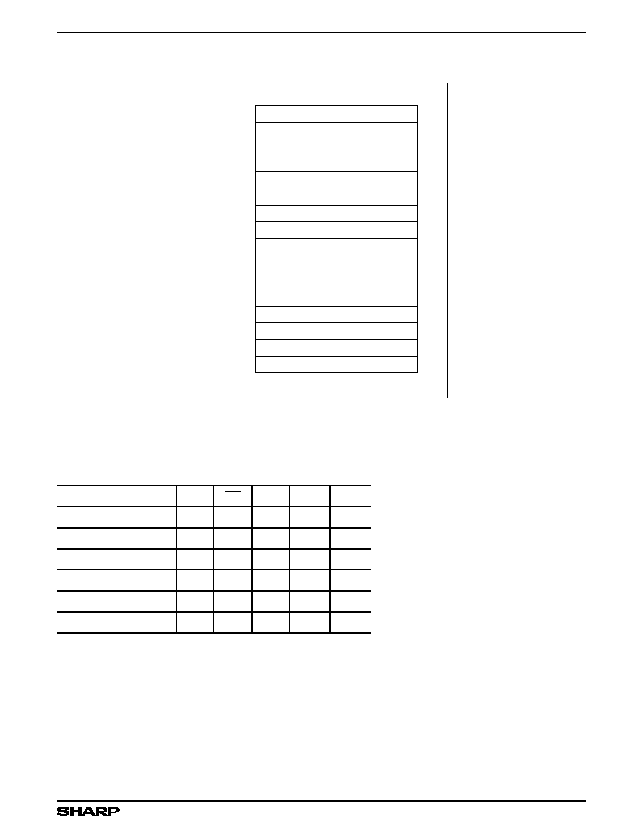
MEMORY MAP
MODE
CE
ª
OE
ª
WE
A
0
DQ
0-7
NOTE
Read
V
IL
V
IL
V
IH
X
D
OUT
1
Output Disable
V
IL
V
IH
V
IH
X
High-Z
1
Standby
V
IH
X
X
X
High-Z
1
Manufacturer ID
V
IL
V
IL
V
IH
V
IL
B0H
2
Device ID
V
IL
V
IL
V
IH
V
IH
ID
2
Write
V
IL
V
IH
V
IL
X
D
IN
1, 3
BUS OPERATIONS, COMMANDS AND STATUS REGISTER DEFINITIONS
Bus Operations
NOTES:
1. X can be V
IH
or V
IL
for address or control pins, which is either V
OL
or V
OH
.
2. A
0
at V
IL
provide manufacturer ID codes. A
0
at V
IH
provide device ID codes.
Device ID Code = 30H. All other addresses are set to zero.
3. Commands for different Erase operations, Data Write operations of Lock-Block
operations can only be successfully completed when V
PP
= V
PPH
.
Figure 4. Chip Memory Map
15
3FFFFH
3C000H
3BFFFH
38000H
37FFFH
34000H
33FFFH
30000H
2FFFFH
2C000H
2BFFFH
28000H
27FFFH
24000H
23FFFH
20000H
1FFFFH
1C000H
1BFFFH
18000H
17FFFH
14000H
13FFFH
10000H
0FFFFH
0C000H
0BFFFH
08000H
07FFFH
04000H
03FFFH
00000H
14
13
12
11
10
9
8
7
6
5
4
3
2
0
16KB BLOCK
16KB BLOCK
16KB BLOCK
16KB BLOCK
16KB BLOCK
16KB BLOCK
16KB BLOCK
16KB BLOCK
16KB BLOCK
16KB BLOCK
16KB BLOCK
16KB BLOCK
16KB BLOCK
16KB BLOCK
1
16KB BLOCK
16KB BLOCK
28F020SUN80-3