LH28F160S5-L/S5H-L
DESCRIPTION
The LH28F160S5-L/S5H-L flash memories with
Smart 5 technology are high-density, low-cost,
nonvolatile, read/write storage solution for a wide
range of applications, having high programming
performance is achieved through highly-optimized
page buffer operations. Their symmetrically-blocked
architecture, flexible voltage and enhanced cycling
capability provide for highly flexible component
suitable for resident flash arrays, SIMMs and
memory cards. Their enhanced suspend
capabilities provide for an ideal solution for code +
data storage applications. For secure code storage
applications, such as networking, where code is
either directly executed out of flash or downloaded
to DRAM, the LH28F160S5-L/S5H-L offer three
levels of protection : absolute protection with V
PP
at
GND, selective hardware block locking, or flexible
software block locking. These alternatives give
designers ultimate control of their code security
needs. The LH28F160S5-L/S5H-L are conformed
to the flash Scalable Command Set (SCS) and the
Common Flash Interface (CFI) specification which
enable universal and upgradable interface, enable
the highest system/device data transfer rates and
minimize device and system-level implementation
costs.
FEATURES
∑ Smart 5 technology
≠ 5 V V
CC
≠ 5 V V
PP
∑ High speed write performance
≠ Two 32-byte page buffers
≠ 2 µs/byte write transfer rate
∑ Common Flash Interface (CFI)
≠ Universal & upgradable interface
∑ Scalable Command Set (SCS)
∑ High performance read access time
LH28F160S5-L70
≠ 70 ns (5.0±0.25 V)/80 ns (5.0±0.5 V)
LH28F160S5H-L70
≠ 70 ns (5.0±0.25 V)/90 ns (5.0±0.5 V)
LH28F160S5-L10/S5H-L10
≠ 100 ns (5.0±0.5 V)
∑ Enhanced automated suspend options
≠ Write suspend to read
≠ Block erase suspend to write
≠ Block erase suspend to read
∑ Enhanced data protection features
≠ Absolute protection with V
PP
= GND
≠ Flexible block locking
≠ Erase/write lockout during power transitions
∑ SRAM-compatible write interface
∑ User-configurable x8 or x16 operation
∑ High-density symmetrically-blocked architecture
≠ Thirty-two 64 k-byte erasable blocks
∑ Enhanced cycling capability
≠ 100 000 block erase cycles
≠ 3.2 million block erase cycles/chip
∑ Low power management
≠ Deep power-down mode
≠ Automatic power saving mode decreases I
CC
in static mode
∑ Automated write and erase
≠ Command user interface
≠ Status register
∑ ETOX
TM
V nonvolatile flash technology
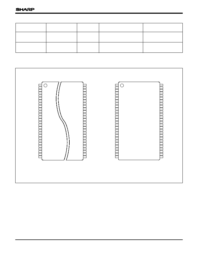
∑ Packages
≠ 56-pin TSOP Type I (TSOP056-P-1420)
Normal bend/Reverse bend
≠ 56-pin SSOP (SSOP056-P-0600)
5
[LH28F160S5-L]
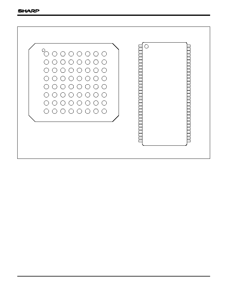
≠ 64-ball CSP (FBGA064-P-0811)
≠ 64-pin SDIP (SDIP064-P-0750)
5
ETOX is a trademark of Intel Corporation.
5
Under development
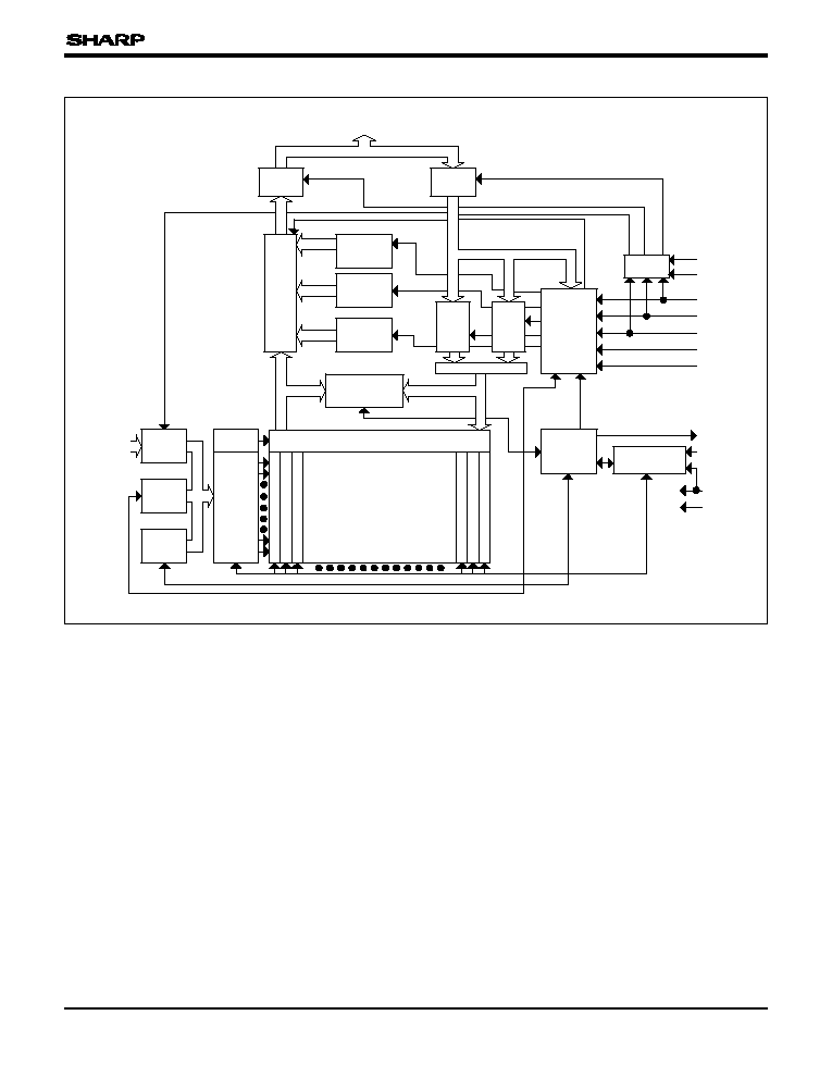
LH28F160S5-L/S5H-L
16 M-bit (2 MB x 8/1 MB x 16) Smart 5
Flash Memories (Fast Programming)
- 1 -
In the absence of confirmation by device specification sheets, SHARP takes no responsibility for any defects that may occur in equipment using any SHARP devices shown in catalogs, data books,
etc. Contact SHARP in order to obtain the latest device specification sheets before using any SHARP device.
LH28F160S5-L/S5H-L
- 5 -
PIN DESCRIPTION
SYMBOL
TYPE
NAME AND FUNCTION
ADDRESS INPUTS : Inputs for addresses during read and write operations. Addresses
are internally latched during a write cycle.
A
0
-A
20
INPUT
A
0 :
Byte Select Address. Not used in x16 mode (can be floated).
A
1
-A
4 :
Column Address. Selects 1 of 16-bit lines.
A
5
-A
15 :
Row Address. Selects 1 of 2 048-word lines.
A
16
-A
20
: Block Address.
DATA INPUT/OUTPUTS :
DQ
0
-DQ
7 :
Inputs data and commands during CUI write cycles; outputs data during
memory array, status register, query, and identifier code read cycles. Data pins float to
high-impedance when the chip is deselected or outputs are disabled. Data is internally
latched during a write cycle.
DQ
8
-DQ
15 :
Inputs data during CUI write cycles in x16 mode; outputs data during memory
array read cycles in x16 mode; not used for status register, query and identifier code read
mode. Data pins float to high-impedance when the chip is deselected, outputs are
disabled, or in x8 mode (BYTE# = V
IL
). Data is internally latched during a write cycle.
CE
0
#, CE
1
#
INPUT
CHIP ENABLE : Activates the device's control logic, input buffers decoders, and sense
amplifiers. Either CE
0
# or CE
1
# V
IH
deselects the device and reduces power
consumption to standby levels. Both CE
0
# and CE
1
# must be V
IL
to select the devices.
RP#
INPUT
RESET/DEEP POWER-DOWN : Puts the device in deep power-down mode and resets
internal automation. RP# V
IH
enables normal operation. When driven V
IL
, RP# inhibits
write operations which provide data protection during power transitions. Exit from deep
power-down sets the device to read array mode.
OE#
INPUT
OUTPUT ENABLE : Gates the device's outputs during a read cycle.
WE#
INPUT
WRITE ENABLE : Controls writes to the CUI and array blocks. Addresses and data are
latched on the rising edge of the WE# pulse.
STS (RY/BY#) : Indicates the status of the internal WSM. When configured in level
mode (default mode), it acts as a RY/BY# pin. When low, the WSM is performing an
internal operation (block erase, full chip erase, (multi) word/byte write or block lock-bit
configuration). STS High Z indicates that the WSM is ready for new commands, block
erase is suspended, and (multi) word/byte write is inactive, (multi) word/byte write is
suspended or the device is in deep power-down mode. For alternate configurations of
the STATUS pin, see the Configuration command (Table 3 and Section 4.14).
WP#
INPUT
WRITE PROTECT : Master control for block locking. When V
IL
, locked blocks can not
be erased and programmed, and block lock-bits can not be set and reset.
BYTE#
INPUT
BYTE ENABLE : BYTE# V
IL
places device in x8 mode. All data are then input or output
on DQ
0-7
, and DQ
8-15
float. BYTE# V
IH
places the device in x16 mode, and turns off the
A
0
input buffer.
BLOCK ERASE, FULL CHIP ERASE, (MULTI) WORD/BYTE WRITE, BLOCK LOCK-
BIT CONFIGURATION POWER SUPPLY : For erasing array blocks, writing bytes or
configuring block lock-bits. With V
PP
V
PPLK
, memory contents cannot be altered. Block
erase, full chip erase, (multi) word/byte write and block lock-bit configuration with an
invalid V
PP
(see Section 6.2.3 "DC CHARACTERISTICS") produce spurious results
and should not be attempted.
V
CC
SUPPLY
DEVICE POWER SUPPLY : Internal detection configures the device for 5 V operation.
Do not float any power pins. With V
CC
V
LKO
, all write attempts to the flash memory
are inhibited. Device operations at invalid V
CC
voltage (see Section 6.2.3 "DC
CHARACTERISTICS") produce spurious results and should not be attempted.
GND
SUPPLY
GROUND : Do not float any ground pins.
NC
NO CONNECT : Lead is not internal connected; recommend to be floated.
DQ
0
-DQ
15
INPUT/
OUTPUT
OPEN
STS
DRAIN
OUTPUT
V
PP
SUPPLY