LH28F320S3TD-L10
LH28F320S3TD-L10
32 M-bit (2 MB x 8/1 MB x 16 x 2-Bank)
Smart 3 Dual Work Flash Memory
DESCRIPTION
The LH28F320S3TD-L10 Dual Work flash memory
with Smart 3 technology is a high-density, low-cost,
nonvolatile, read/write storage solution for a wide
range of applications, having high programming
performance is achieved through highly-optimized
page buffer operations. Its symmetrically-blocked
architecture, flexible voltage and enhanced cycling
capability provide for highly flexible component
suitable for resident flash arrays, SIMMs and
memory cards. Its enhanced suspend capabilities
provide for an ideal solution for code + data storage
applications. For secure code storage applications,
such as networking, where code is either directly
executed out of flash or downloaded to DRAM, the
LH28F320S3TD-L10 offers three levels of
protection : absolute protection with V
PP
at GND,
selective hardware block locking, or flexible
software block locking. These alternatives give
designers ultimate control of their code security
needs. LH28F320S3TD-L10 is conformed to the
flash Scalable Command Set (SCS) and the
Common Flash Interface (CFI) specification which
enable universal and upgradable interface, enable
the highest system/device data transfer rates and
minimize device and system-level implementation
costs.
FEATURES
∑ Smart 3 Dual Work technology
≠ 2.7 V or 3.3 V V
CC
≠ 2.7 V, 3.3 V or 5 V V
PP
≠ Capable of performing erase, write and read
for each bank independently (Impossible to
perform read from both banks at a time).
∑ High-speed write performance
≠ Two 32-byte page buffers/bank
≠ 2.7 µs/byte write transfer rate
∑ Common Flash Interface (CFI)
≠ Universal & upgradable interface
∑ Scalable Command Set (SCS)
∑ High performance read access time
≠ 100 ns (3.3±0.3 V)/120 ns (2.7 to 3.6 V)
∑ Enhanced automated suspend options
≠ Write suspend to read
≠ Block erase suspend to write
≠ Block erase suspend to read
∑ Enhanced data protection features
≠ Absolute protection with V
PP
= GND
≠ Flexible block locking
≠ Erase/write lockout during power transitions
∑ SRAM-compatible write interface
∑ User-configurable x8 or x16 operation
∑ High-density symmetrically-blocked architecture
≠ Sixty-four 64 k-byte erasable blocks
∑ Enhanced cycling capability
≠ 100 000 block erase cycles
≠ 3.2 million block erase cycles/bank
∑ Low power management
≠ Deep power-down mode
≠ Automatic power saving mode decreases Icc
in static mode
∑ Automated write and erase
≠ Command user interface
≠ Status register
∑ ETOX
TM
V nonvolatile flash technology
∑ Package
≠ 56-pin TSOP Type I (TSOP056-P-1420)
Normal bend
ETOX is a trademark of Intel Corporation.
- 1 -
In the absence of confirmation by device specification sheets, SHARP takes no responsibility for any defects that may occur in equipment using any SHARP devices shown in catalogs, data books,
etc. Contact SHARP in order to obtain the latest device specification sheets before using any SHARP device.

- 2 -
LH28F320S3TD-L10
PIN CONNECTIONS
56-PIN TSOP (Type I)
(TSOP056-P-1420)
1
2
3
4
5
6
7
8
9
10
11
12
13
14
15
16
17
18
19
20
21
22
23
24
25
26
27
28
56
55
54
53
52
51
50
49
48
47
46
45
44
43
42
41
40
39
38
37
36
35
34
33
32
31
30
29
NC
BE
1L
#
BE
1H
#
A
20
A
19
A
18
A
17
A
16
V
CC
A
15
A
14
A
13
A
12
BE
0
#
V
PP
RP#
A
11
A
10
A
9
A
8
GND
A
7
A
6
A
5
A
4
A
3
A
2
A
1
WP#
WE#
OE#
STS
DQ
15
DQ
7
DQ
14
DQ
6
GND
DQ
13
DQ
5
DQ
12
DQ
4
V
CC
GND
DQ
11
DQ
3
DQ
10
DQ
2
V
CC
DQ
9
DQ
1
DQ
8
DQ
0
A
0
BYTE#
NC
NC
TOP VIEW
- 3 -
LH28F320S3TD-L10
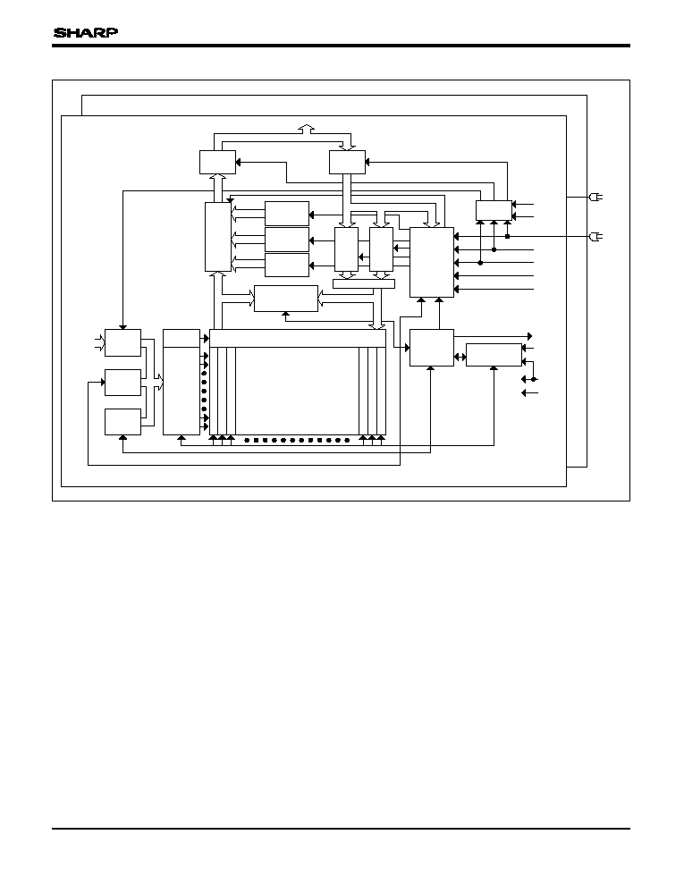
BLOCK DIAGRAM
Y GATING
Y
DECODER
INPUT
BUFFER
OUTPUT
BUFFER
DQ
0
-DQ
15
V
CC
WE#
OE#
RP#
WP#
ADDRESS
LATCH
DATA
COMPARATOR
PROGRAM/ERASE
VOLTAGE SWITCH
STATUS
REGISTER
COMMAND
USER
INTERFACE
MULTIPLEXER
WRITE
STATE
MACHINE
DATA
REGISTER
DATA
REGISTER
OUTPUT
MULTIPLEXER
QUERY
ROM
ADDRESS
COUNTER
A
0
-A
20
X
DECODER
32
64 k-BYTE
BLOCKS
BYTE#
V
CC
GND
V
PP
STS
INPUT
BUFFER
I/O
LOGIC
Bank0
Bank1
BE
0
#
BE
1L
#
BE
0
#
BE
1H
#
IDENTIFIER
REGISTER

- 4 -
LH28F320S3TD-L10
SYMBOL
TYPE
NAME AND FUNCTION
ADDRESS INPUTS : Inputs for addresses during read and write operations. Addresses
are internally latched during a write cycle.
A
0
: Byte Select Address. Not used in x16 mode (can be floated).
A
1
-A
4
: Column Address. Selects 1 of 16-bit lines.
A
5
-A
15
: Row Address. Selects 1 of 2 048-word lines.
A
16
-A
20
: Block Address.
DATA INPUT/OUTPUTS :
DQ
0
-DQ
7
: Inputs data and commands during CUI write cycles; outputs data during
memory array, status register, query, and identifier code read cycles. Data pins float to
high-impedance when the chip is deselected or outputs are disabled. Data is internally
latched during a write cycle.
DQ
8
-DQ
15
: Inputs data during CUI write cycles in x16 mode; outputs data during
memory array read cycles in x16 mode; not used for status register, query and identifier
code read mode. Data pins float to high-impedance when the chip is deselected, outputs
are disabled, or in x8 mode (BYTE# = V
IL
). Data is internally latched during a write cycle.
BANK ENABLE : Activates the device's control logic, input buffers, decoders, and sense
amplifiers. When BE
0
# and BE
1L
# "low", bank0 is in active. When BE
0
# and BE
1H
# are
"low", bank1 is in active. BE
0
# and BE
1L
#, BE
1H
# must not be low at the same time.
RP#
INPUT
RESET/DEEP POWER-DOWN : Puts the device in deep power-down mode and resets
internal automation. RP# V
IH
enables normal operation. When driven V
IL
, RP# inhibits
write operations which provide data protection during power transitions. Exit from deep
power-down sets the device to read array mode.
OE#
INPUT
OUTPUT ENABLE : Gates the device's outputs during a read cycle.
WE#
INPUT
WRITE ENABLE : Controls writes to the CUI and array blocks. Addresses and data are
latched on the rising edge of the WE# pulse.
STS (RY/BY#) : Indicates the status of the internal WSM. When configured in level
mode (default mode) , it acts as a RY/BY# pin. When low, the WSM is performing an
internal operation (block erase, bank erase, (multi) word/byte write or block lock-bit
configuration). STS High Z indicates that the WSM is ready for new commands, block
ease is suspended, and (multi) word/byte write is inactive, (multi) word/byte write is
suspended or the device is in deep power-down mode. For alternate configurations of
the STATUS pin, see the Configuration command (Table 3 and Section 4.14).
WP#
INPUT
WRITE PROTECT : Master control for block locking. When V
IL
, locked blocks can not
be erased and programmed, and block lock-bits can not be set and reset.
BYTE#
INPUT
BYTE ENABLE : BYTE# V
IL
places device in x8 mode. All data are then input or output
on DQ
0-7
, and DQ
8-15
float. BYTE# V
IH
places the device in x16 mode, and turns off the
A
0
input buffer.
BLOCK ERASE, BANK ERASE, (MULTI) WORD/BYTE WRITE, BLOCK LOCK-BIT
CONFIGURATION POWER SUPPLY : For erasing array blocks, writing bytes or
configuring block lock-bits. With V
PP
V
PPLK
, memory contents cannot be altered. Block
erase, bank erase, word/byte write, and block lock-bit configuration with an invalid V
PP
(see Section 6.2.3 "DC CHARACTERISTICS") produce spurious results and should
not be attempted.
DEVICE POWER SUPPLY : Internal detection configures the device for 2.7 V or 3.3 V
operation. To switch from one voltage to another, ramp V
CC
down to GND and then ramp
V
CC
to the new voltage. Do not float any power pins. With V
CC
V
LKO
, all write attempts
to the flash memory are inhibited. Device operations at invalid V
CC
voltage (see Section
6.2.3 "DC CHARACTERISTICS") produce spurious results and should not be attempted.
GND
SUPPLY
GROUND : Do not float any ground pins.
NC
NO CONNECT : Lead is not internal connected; recommend to be floated.
DQ
0
-DQ
15
INPUT/
OUTPUT
OPEN
STS
DRAIN
OUTPUT
A
0
-A
20
INPUT
V
PP
SUPPLY
V
CC
SUPPLY
PIN DESCRIPTION
BE
0
#,
INPUT
BE
1L
#, BE
1H
#

LH28F320S3TD-L10
1 INTRODUCTION
This datasheet contains LH28F320S3TD-L10
specifications. Section 1 provides a flash memory
overview. Sections 2, 3, 4, and 5 describe the memory
organization and functionality. Section 6 covers
electrical specifications. The LH28F320S3TD-L10
flash memory documentation also includes ordering
information which is referenced in Section 7.
1.1
Product Overview
The LH28F320S3TD-L10 is a high-performance
32 M-bit Smart 3 Dual Work flash memory
organized as 2 MB x8/1 MB x 16 x 2-Bank. The
4 MB of data is arranged in sixty-four 64 k-byte
blocks which are individually erasable, lockable,
and unlockable in-system. The memory map is
shown in Fig. 1.
Smart 3 technology provides a choice of V
CC
and
V
PP
combinations, as shown in Table 1, to meet
system performance and power expectations. V
PP
at 2.7 V, 3.3 V and 5 V eliminates the need for a
separate 12 V converter. In addition to flexible
erase and program voltages, the dedicated V
PP
pin
gives complete data protection when V
PP
V
PPLK
.
Table 1 V
CC
and V
PP
Voltage Combinations
Offered by Smart 3 Technology
Internal V
CC
and V
PP
detection circuitry auto-
matically configures the device for optimized read
and write operations.
A Command User Interface (CUI) serves as the
interface between the system processor and internal
operation of the device. A valid command sequence
written to the CUI initiates device automation. An
internal Write State Machine (WSM) automatically
executes the algorithms and timings necessary for
block erase, bank erase, (multi) word/byte write and
block lock-bit configuration operations.
A block erase operation erases one of the device's
64 k-byte blocks typically within 0.41 second (3.3 V
V
CC
, 5 V V
PP
) independent of other blocks. Each
block can be independently erased 100 000 times
(3.2 million block erases per bank). Block erase
suspend mode allows system software to suspend
block erase to read data from, or write data to any
other block.
A word/byte write is performed in byte increments
typically within 12.95 µs (3.3 V V
CC
, 5 V V
PP
). A
multi word/byte write has high speed write
performance of 2.7 µs/byte (3.3 V V
CC
, 5 V V
PP
).
(Multi) word/byte write suspend mode enables the
system to read data from, or write data to any other
flash memory array location.
Individual block locking uses a combination of bits
and WP#, sixty-four block lock-bits per bank, to lock
and unlock blocks. Block lock-bits gate block erase,
bank erase and (multi) word/byte write operations.
Block lock-bit configuration operations (Set Block
Lock-Bit and Clear Block Lock-Bits commands) set
and cleared block lock-bits.
The status register indicates when the WSM's block
erase, bank erase, (multi) word/byte write or block
lock-bit configuration operation is finished.
The STS output gives an additional indicator of
WSM activity by providing both a hardware signal
of status (versus software polling) and status
masking (interrupt masking for background block
erase, for example). Status polling using STS
minimizes both CPU overhead and system power
consumption. STS pin can be configured to
different states using the Configuration command.
The STS pin defaults to RY/BY# operation. When
low, STS indicates that the WSM is performing a
block erase, bank erase, (multi) word/byte write or
block lock-bit configuration. STS High Z indicates
that the WSM is ready for a new command, block
erase is suspended and (multi) word/byte write are
V
CC
VOLTAGE
V
PP
VOLTAGE
2.7 V
2.7 V, 3.3 V, 5 V
3.3 V
3.3 V, 5 V
- 5 -