- 1 -
In the absence of confirmation by device specification sheets, SHARP takes no responsibility for any defects that may occur in equipment using any SHARP devices shown in catalogs, data books,
etc. Contact SHARP in order to obtain the latest device specification sheets before using any SHARP device.
LH28F800BG-L
(FOR SOP)
8 M-bit (512 kB x 16) SmartVoltage
Flash Memory
LH28F800BG-L (FOR SOP)
DESCRIPTION
The LH28F800BG-L flash memory with Smart
Voltage technology is a high-density, low-cost,
nonvolatile, read/write storage solution for a wide
range of applications. The LH28F800BG-L can
operate at V
CC
= 2.7 V and V
PP
= 2.7 V. Its low
voltage operation capability realizes longer battery
life and suits for cellular phone application. Its boot,
parameter and main-blocked architecture, flexible
voltage and enhanced cycling capability provide for
highly flexible component suitable for portable
terminals and personal computers. Its enhanced
suspend capabilities provide for an ideal solution for
code + data storage applications. For secure code
storage applications, such as networking, where
code is either directly executed out of flash or
downloaded to DRAM, the LH28F800BG-L offers
two levels of protection : absolute protection with
V
PP
at GND, selective hardware boot block locking.
These alternatives give designers ultimate control of
their code security needs.
FEATURES
∑ SmartVoltage technology
≠ 2.7 V, 3.3 V or 5 V V
CC
≠ 2.7 V, 3.3 V, 5 V or 12 V V
PP
∑ High performance read access time
LH28F800BG-L85
≠ 85 ns (5.0±0.25 V)/90 ns (5.0±0.5 V)/
100 ns (3.3±0.3 V)/120 ns (2.7 to 3.6 V)
LH28F800BG-L12
≠ 120 ns (5.0±0.5 V)/130 ns (3.3±0.3 V)/
150 ns (2.7 to 3.6 V)
∑ Enhanced automated suspend options
≠ Word write suspend to read
≠ Block erase suspend to word write
≠ Block erase suspend to read
∑ Enhanced data protection features
≠ Absolute protection with V
PP
= GND
≠ Block erase/word write lockout during power
transitions
≠ Boot blocks protection except RP# = V
HH
∑ SRAM-compatible write interface
∑ Optimized array blocking architecture
≠ Two 4 k-word boot blocks
≠ Six 4 k-word parameter blocks
≠ Fifteen 32 k-word main blocks
≠ Top or bottom boot location
∑ Enhanced cycling capability
≠ 100 000 block erase cycles
∑ Low power management
≠ Deep power-down mode
≠ Automatic power saving mode decreases I
CC
in static mode
∑ Automated word write and block erase
≠ Command user interface
≠ Status register
∑ ETOX
TM
V nonvolatile flash technology
∑ Package
≠ 44-pin SOP (SOP044-P-0600)
ETOX is a trademark of Intel Corporation.
LH28F800BG-L (FOR SOP)
- 2 -
PIN CONNECTIONS
44-PIN SOP
(SOP044-P-0600)
V
PP
A
18
A
17
A
7
A
6
A
5
A
4
A
3
A
2
A
1
A
0
CE#
GND
OE#
DQ
0
DQ
8
DQ
1
DQ
9
DQ
2
DQ
10
DQ
3
DQ
11
1
2
3
4
5
6
7
8
9
10
11
12
13
14
15
16
17
18
19
20
21
22
44
43
42
41
40
39
38
37
36
35
34
33
32
31
30
29
28
27
26
25
24
23
RP#
WE#
A
8
A
9
A
10
A
11
A
12
A
13
A
14
A
15
A
16
NC
GND
DQ
15
DQ
7
DQ
14
DQ
6
DQ
13
DQ
5
DQ
12
DQ
4
V
CC
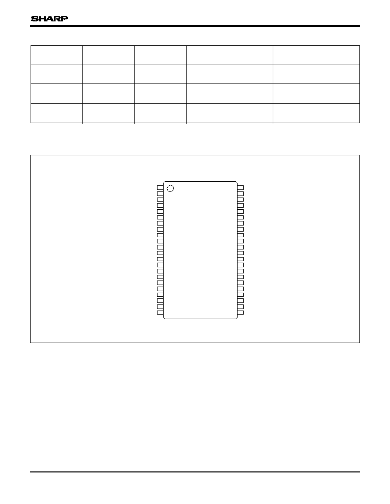
COMPARISON TABLE
1 Refer to the datasheet of LH28F800BG-L/BGH-L (FOR TSOP, CSP).
TOP VIEW
VERSIONS
OPERATING
PACKAGE
DC CHARACTERISTICS
WRITE PROTECT FUNCTION
TEMPERATURE
V
CC
deep power-down current (MAX.)
FOR BOOT BLOCKS
LH28F800BG-L
0 to +70∞C
44-pin SOP
10 µA
Controlled by RP# pin
(FOR SOP)
LH28F800BG-L
1
0 to +70∞C
48-pin TSOP (I)
10 µA
Controlled by
(FOR TSOP, CSP)
48-ball CSP
WP# and RP# pins
LH28F800BGH-L
1
≠40 to +85∞C
48-pin TSOP (I)
20 µA
Controlled by
(FOR TSOP, CSP)
48-ball CSP
WP# and RP# pins
LH28F800BG-L (FOR SOP)
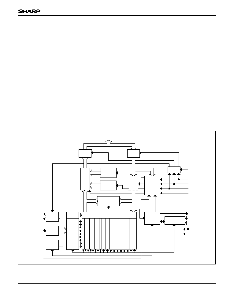
BLOCK ORGANIZATION
This product features an asymmetrically-blocked
architecture providing system memory integration.
Each erase block can be erased independently of
the others up to 100 000 times. For the address
locations of the blocks, see the memory map in
Fig. 1.
Boot Blocks : The two boot blocks are intended to
replace a dedicated boot PROM in a micro-
processor or microcontroller-based system. The
boot blocks of 4 k words (4 096 words) feature
hardware controllable write-protection to protect the
crucial microprocessor boot code from accidental
modification. The protection of the boot blocks is
controlled using a combination of the V
PP
and RP#
pins.
Parameter Blocks : The boot block architecture
includes parameter blocks to facilitate storage of
frequently update small parameters that would
normally require an EEPROM. By using software
techniques, the byte-rewrite functionality of
EEPROMs can be emulated. Each boot block
component contains six parameter blocks of 4 k
words (4 096 words) each. The parameter blocks
are not write-protectable.
Main Blocks : The reminder is divided into main
blocks for data or code storage. Each 8 M-bit
device contains fifteen 32 k words (32 768 words)
blocks.
- 3 -
INPUT
BUFFER
BUFFER
OUTPUT
MULTIPLEXER
V
CC
CE#
RP#
OE#
IDENTIFIER
REGISTER
COMMAND
USER
INTERFACE
WRITE
STATE
MACHINE
PROGRAM/ERASE
VOLTAGE SWITCH
I/O
LOGIC
STATUS
REGISTER
DATA
REGISTER
DATA
COMPARATOR
15
32 k-WORD
MAIN BLOCKS
X
DECODER
Y
DECODER
Y GATING
RY/BY#
V
PP
V
CC
GND
DQ
0
-DQ
15
A
0
-A
18
INPUT
BUFFER
ADDRESS
LATCH
ADDRESS
COUNTER
WE#
OUTPUT
BOOT BLOCK 0
BOOT BLOCK 1
PARAMETER BLOCK 0
PARAMETER BLOCK 1
PARAMETER BLOCK 2
PARAMETER BLOCK 3
PARAMETER BLOCK 4
PARAMETER BLOCK 5
MAIN BLOCK 0
MAIN BLOCK 1
MAIN BLOCK 13
MAIN BLOCK 14
BLOCK DIAGRAM
- 4 -
LH28F800BG-L (FOR SOP)
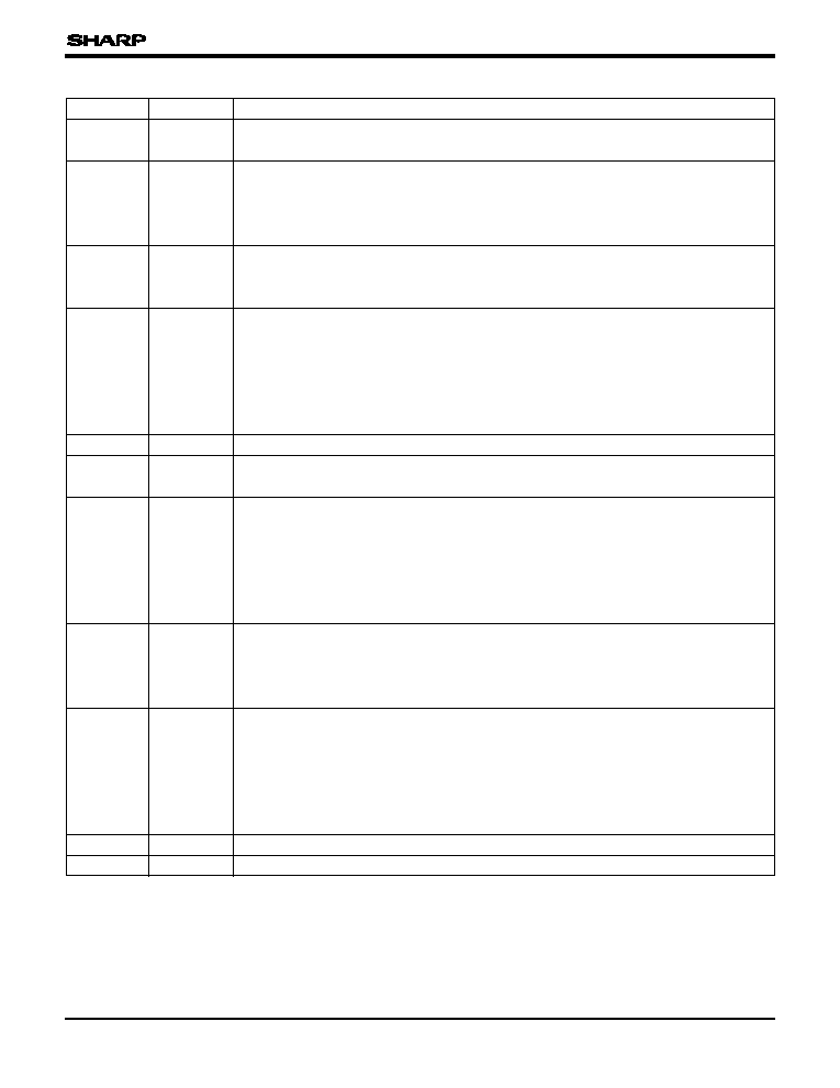
SYMBOL
TYPE
NAME AND FUNCTION
A
0
-A
18
INPUT
ADDRESS INPUTS : Inputs for addresses during read and write operations. Addresses
are internally latched during a write cycle.
DATA INPUT/OUTPUTS : Inputs data and commands during CUI write cycles; outputs
data during memory array, status register and identifier code read cycles. Data pins float
to high-impedance when the chip is deselected or outputs are disabled. Data is
internally latched during a write cycle.
CE#
INPUT
CHIP ENABLE : Activates the device's control logic, input buffers, decoders and sense
amplifiers. CE#-high deselects the device and reduces power consumption to standby
levels.
RESET/DEEP POWER-DOWN : Puts the device in deep power-down mode and resets
internal automation. RP#-high enables normal operation. When driven low, RP# inhibits
write operations which provide data protection during power transitions. Exit from deep
power-down sets the device to read array mode. With RP# = V
HH
, block erase or word
write can operate to all blocks. Block erase or word write with V
IH
< RP# < V
HH
produce
spurious results and should not be attempted.
OE#
INPUT
OUTPUT ENABLE : Gates the device's outputs during a read cycle.
WE#
INPUT
WRITE ENABLE : Controls writes to the CUI and array blocks. Addresses and data are
latched on the rising edge of the WE# pulse.
READY/BUSY : Indicates the status of the internal WSM. When low, the WSM is
performing an internal operation (block erase or word write). RY/BY#-high indicates that
the WSM is ready for new commands, block erase is suspended, and word write is
inactive, word write is suspended, or the device is in deep power-down mode. RY/BY#
is always active and does not float when the chip is deselected or data outputs are
disabled.
V
PP
SUPPLY
BLOCK ERASE AND WORD WRITE POWER SUPPLY : For erasing array blocks or
writing words. With V
PP
V
PPLK
, memory contents cannot be altered. Block erase and
word write with an invalid V
PP
(see Section 6.2.3 "DC CHARACTERISTICS") produce
spurious results and should not be attempted.
DEVICE POWER SUPPLY : Internal detection configures the device for 2.7 V, 3.3 V or
5 V operation. To switch from one voltage to another, ramp V
CC
down to GND and then
ramp V
CC
to the new voltage. Do not float any power pins. With V
CC
V
LKO
, all write
attempts to the flash memory are inhibited. Device operations at invalid V
CC
voltage
(see Section 6.2.3 "DC CHARACTERISTICS") produce spurious results and should
not be attempted.
GND
SUPPLY
GROUND : Do not float any ground pins.
NC
NO CONNECT : Lead is not internal connected; recommend to be floated.
PIN DESCRIPTION
DQ
0
-DQ
15
INPUT/
OUTPUT
RP#
INPUT
RY/BY#
OUTPUT
V
CC
SUPPLY
LH28F800BG-L (FOR SOP)
1 INTRODUCTION
This datasheet contains LH28F800BG-L speci-
fications. Section 1 provides a flash memory
overview. Sections 2, 3, 4 and 5 describe the
memory organization and functionality. Section 6
covers electrical specifications. LH28F800BG-L
flash memory documentation also includes ordering
information which is referenced in Section 7.
1.1
New Features
Key enhancements of LH28F800BG-L SmartVoltage
flash memory are :
∑ SmartVoltage Technology
∑ Enhanced Suspend Capabilities
∑ Boot Block Architecture
Note following important differences :
∑ V
PPLK
has been lowered to 1.5 V to support
2.7 V, 3.3 V and 5 V block erase and word
write operations. Designs that switch V
PP
off
during read operations should make sure that
the V
PP
voltage transitions to GND.
∑ To take advantage of SmartVoltage technology,
allow V
PP
connection to 2.7 V, 3.3 V or 5 V.
1.2
Product Overview
The LH28F800BG-L is a high-performance 8 M-bit
SmartVoltage flash memory organized as 512 k-
word of 16 bits. The 512 k-word of data is arranged
in two 4 k-word boot blocks, six 4 k-word parameter
blocks and fifteen 32 k-word main blocks which are
individually erasable in-system. The memory map is
shown in Fig. 1.
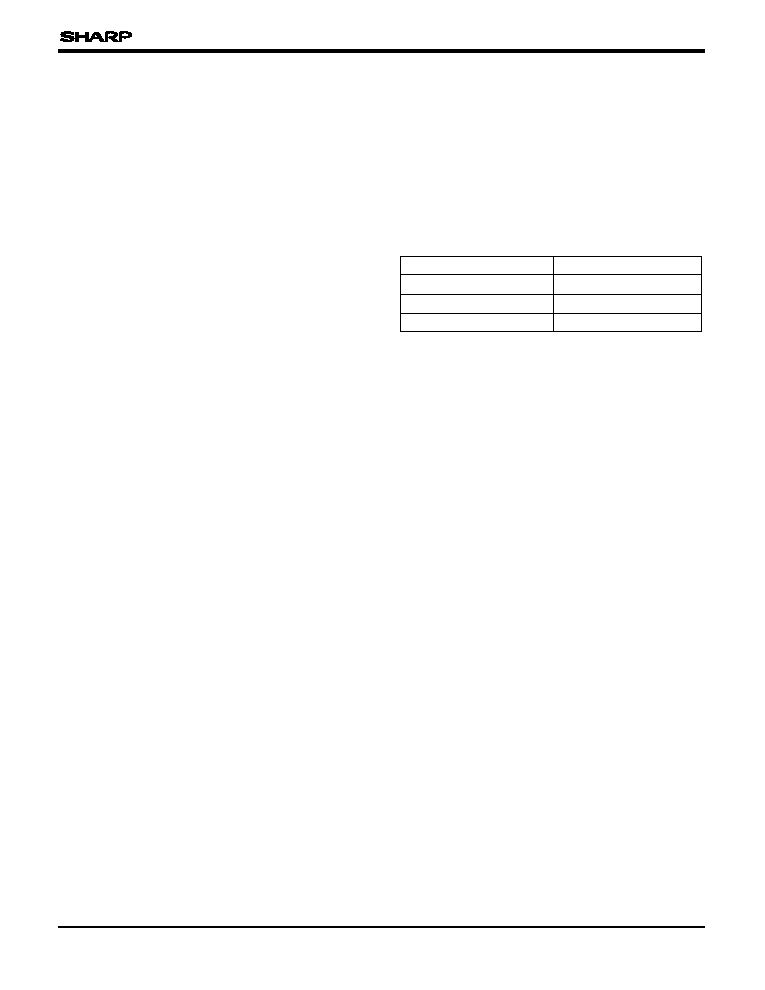
SmartVoltage technology provides a choice of V
CC
and V
PP
combinations, as shown in Table 1, to
meet system performance and power expectations.
2.7 V V
CC
consumes approximately one-fifth the
power of 5 V V
CC
and 3.3 V V
CC
consumes
approximately one-fourth the power of 5 V V
CC
.
But, 5 V V
CC
provides the highest read
performance. V
PP
at 2.7 V, 3.3 V and 5 V
eliminates the need for a separate 12 V converter,
while V
PP =
12 V maximizes block erase and word
write performance. In addition to flexible erase and
program voltages, the dedicated V
PP
pin gives
complete data protection when V
PP
V
PPLK
.
Table 1 V
CC
and V
PP
Voltage Combinations
Offered by SmartVoltage Technology
Internal V
CC
and V
PP
detection circuitry auto-
matically configures the device for optimized read
and write operations.
A Command User Interface (CUI) serves as the
interface between the system processor and
internal operation of the device. A valid command
sequence written to the CUI initiates device
automation. An internal Write State Machine (WSM)
automatically executes the algorithms and timings
necessary for block erase and word write
operations.
A block erase operation erases one of the device's
32 k-word blocks typically within 0.39 second (5 V
V
CC
, 12 V V
PP
), 4 k-word blocks typically within
0.25 second (5 V V
CC
, 12 V V
PP
) independent of
other blocks. Each block can be independently
erased 100 000 times. Block erase suspend mode
allows system software to suspend block erase to
read data from, or write data to any other block.
Writing memory data is performed in word increments
of the device's 32 k-word blocks typically within 8.4 µs
(5 V V
CC
, 12 V V
PP
), 4 k-word blocks typically within
17 µs (5 V V
CC
, 12 V V
PP
). Word write suspend
mode enables the system to read data from, or write
data to any other flash memory array location.
V
CC
VOLTAGE
V
PP
VOLTAGE
2.7 V
2.7 V, 3.3 V, 5 V, 12 V
3.3 V
3.3 V, 5 V, 12 V
5 V
5 V, 12 V
- 5 -