LH28F800SU
1
8M (512K ◊ 16, 1M ◊ 8) Flash Memory
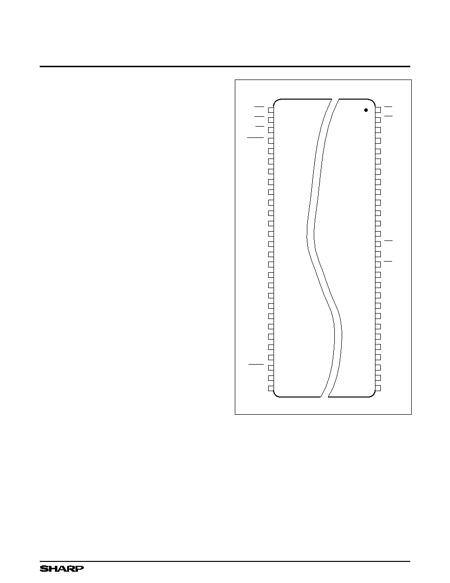
Figure 1. TSOP Reverse Bend Configuration
FEATURES
∑
User-Configurable x8 or x16 Operation
∑
User-Selectable 3.3 V or 5 V V
CC
∑
5 V Write/Erase Operations (5 V V
PP
)
≠ No Requirement for DC/DC
Converter to Write/Erase
∑
70 ns Maximum Access Time
∑
Minimum 2.7 V Read capability
≠ 160 ns Maximum Access Time
(V
CC
= 2.7 V)
∑
16 Independently Lockable Blocks
∑
0.32 MB/sec Write Transfer Rate
∑
100,000 Erase Cycles per Block
∑
Revolutionary Architecture
≠ Pipelined Command Execution
≠ Write During Erase
≠ Command Superset of
Sharp LH28F008SA
∑
5 µA (TYP.) I
CC
in CMOS Standby
∑
1 µA (TYP.) Deep Power-Down
∑
State-of-the-Art 0.55 µm ETOXTM
Flash Technology
∑
56-Pin, 1.2 mm ◊ 14 mm ◊ 20 mm
TSOP (Type I) Package
28F800SUR-1
TOP VIEW
56-PIN TSOP
2
3
4
5
8
9
A
16
A
19
53
52
51
50
49
48
45
42
NC
NC
6
7
A
17
A
18
47
46
RY/BY
DQ
15
DQ
14
GND
GND
10
11
12
55
54
OE
V
CC
13
44
DQ
4
43
V
CC
A
15
DQ
7
14
15
16
17
18
19
20
39
36
41
40
38
37
DQ
3
DQ
10
DQ
2
V
CC
A
10
A
9
A
11
V
PP
RP
CE
0
A
8
DQ
9
WE
DQ
6
DQ
13
DQ
11
56
1
CE
1
3/5
WP
21
22
23
24
25
26
27
28
A
4
A
3
A
5
A
7
A
6
GND
A
2
A
1
34
DQ
8
35
DQ
1
31
33
32
30
29
A
0
BYTE
NC
NC
DQ
0
A
14
A
13
A
12
DQ
5
DQ
12
LH28F800SU
8M (512K ◊ 16, 1M ◊ 8) Flash Memory
2
INTRODUCTION
Sharp's LH28F800SU 8M Flash Memory is a revolu-
tionary architecture which enables the design of truly
mobile, high performance, personal computing and com-
munication products. With innovative capabilities, 5 V
single voltage operation and very high read/write per-
formance, the LH28F800SU is also the ideal choice for
designing embedded mass storage flash memory sys-
tems.
The LH28F800SU is a very high density, highest per-
formance non-volatile read/write solution for solid-state
storage applications. Its symmetrically blocked archi-
tecture (100% compatible with the LH28F008SA 8M
Flash memory, the LH28F016SA 16M Flash memory
and the LH28F016SU 16M 5 V single voltage Flash
memory), extended cycling, low power 3.3 V operation,
very fast write and read performance and selective block
locking provide a highly flexible memory component suit-
able for high density memory cards, Resident Flash
Arrays and PCMCIA-ATA Flash Drives. The
LH28F800SU's dual read voltage enables the design of
memory cards which can interchangeably be read/writ-
ten in 3.3 V and 5.0 V systems. Its x8/x16 architecture
allows the optimization of memory to processor inter-
face. The flexible block locking option enables bundling
of executable application software in a Resident Flash
Array or memory card. Manufactured on Sharp's 0.55
µm ETOXTM process technology, the LH28F800SU is
the most cost-effective, high-density 3.3 V flash memory.
DESCRIPTION
The LH28F800SU is a high performance 8M
(8,388,608 bit) block erasable non-volatile random
access memory organized as either 512K ◊ 16 or
1M ◊ 8. The LH28F800SU includes sixteen 64K (65,536)
blocks or sixteen 32-KW (32,768) blocks. A chip memory
map is shown in Figure 3.
The implementation of a new architecture, with many
enhanced features, will improve the device operating
characteristics and results in greater product reliability
and ease of use.
Among the significant enhancements of the
LH28F800SU:
∑
5 V Write/Erase Operation (5 V V
PP
)
∑
3.3 V Low Power Capability (2.7 V V
CC
Read)
∑
Improved Write Performance
∑
Dedicated Block Write/Erase Protection
A 3/5
ª
input pin reconfigures the device internally for
optimized 3.3 V or 5.0 V read/write operation.
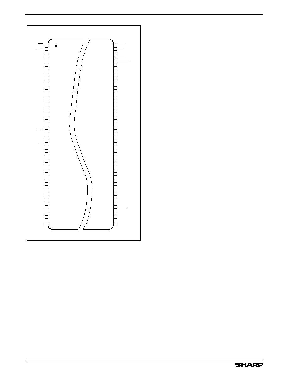
Figure 2. TSOP Configuration
28F800SUR-17
TOP VIEW
56-PIN TSOP
2
3
4
5
8
9
A
16
A
19
53
52
51
50
49
48
45
42
NC
NC
6
7
A
17
A
18
47
46
RY/BY
DQ
15
DQ
14
GND
GND
10
11
12
55
54
OE
V
CC
13
44
DQ
4
43
V
CC
A
15
DQ
7
14
15
16
17
18
19
20
39
36
41
40
38
37
DQ
3
DQ
10
DQ
2
V
CC
A
10
A
9
A
11
V
PP
RP
CE
0
A
8
DQ
9
WE
DQ
6
DQ
13
DQ
11
56
1
CE
1
3/5
WP
21
22
23
24
25
26
27
28
A
4
A
3
A
5
A
7
A
6
GND
A
2
A
1
34
DQ
8
35
DQ
1
31
33
32
30
29
A
0
BYTE
NC
NC
DQ
0
A
14
A
13
A
12
DQ
5
DQ
12
8M (512K ◊ 16, 1M ◊ 8) Flash Memory
LH28F800SU
3
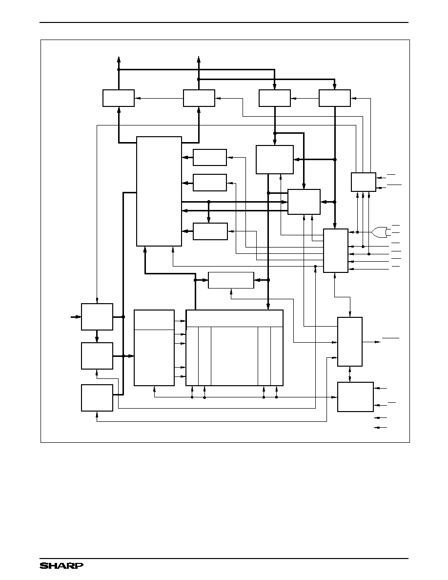
Figure 3. LH28F800SU Block Diagram (Architectural Evolution Includes Page Buffers,
Queue Registers and Extended Status Registers)
OUTPUT
BUFFER
OUTPUT
BUFFER
INPUT
BUFFER
INPUT
BUFFER
DQ
0
-
DQ
7
DQ
8
-
DQ
15
ID
REGISTER
OUTPUT
MULTIPLEXER
CSR
ESRs
DATA
COMPARATOR
DATA
QUEUE
REGISTERS
PAGE
BUFFERS
CUI
WSM
64KB BLOCK 0
64KB BLOCK 1
64KB BLOCK 14
64KB BLOCK 15
. . .
. . .
Y GATING/SENSING
Y-DECODER
X-DECODER
PROGRAM/
ERASE
VOLTAGE
SWITCH
V
PP
3/5
V
CC
GND
RY/BY
ADDRESS
COUNTER
ADDRESS
QUEUE
LATCHES
INPUT
BUFFER
A
0
- A
19
. . .
28F800SUR-2
I/O
LOGIC
RP
WP
WE
OE
CE
0
CE
1
3/5
BYTE
LH28F800SU
8M (512K ◊ 16, 1M ◊ 8) Flash Memory
4
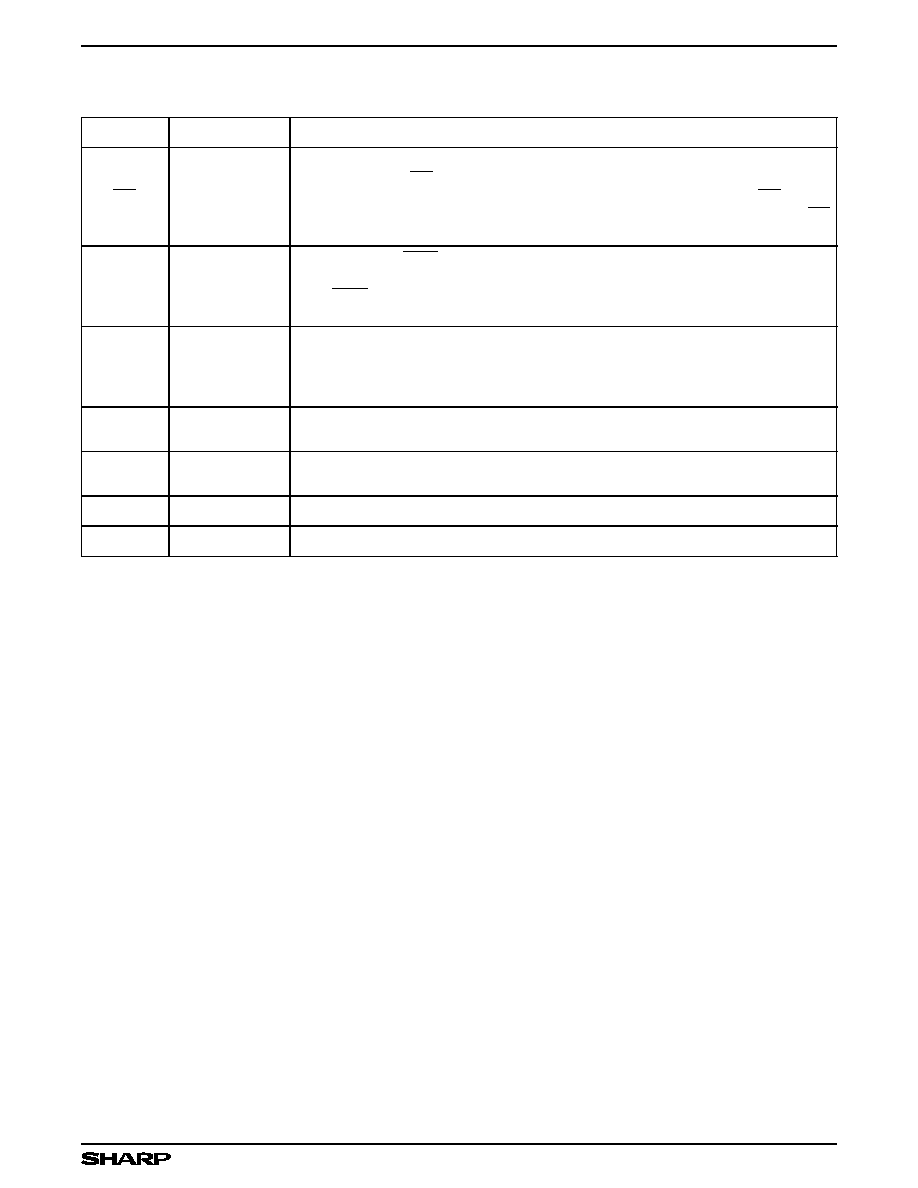
PIN DESCRIPTION
SYMBOL
TYPE
NAME AND FUNCTION
A
0
INPUT
BYTE-SELECT ADDRESS:
Selects between high and low byte when device is in x8
mode. This address is latched in x8 Data Writes. Not used in x16 mode (i.e., the
A
0
input buffer is turned off when BYTE is high).
A
1
- A
15
INPUT
WORD-SELECT ADDRESSES:
Select a word within one 64K block. A
6
- A
15
selects
1 of 1024 rows, and A
1
- A
5
selects 16 of 512 columns. These addresses are
latched during Data Writes.
A
16
- A
19
INPUT
BLOCK-SELECT ADDRESSES:
Select 1 of 16 Erase blocks. These addresses are
latched during Data Writes, Erase and Lock-Block operations.
DQ
0
- DQ
7
INPUT/OUTPUT
LOW-BYTE DATA BUS:
Inputs data and commands during CUI write cycles.
Outputs array, buffer, identifier or status data in the appropriate Read mode. Floated
when the chip is de-selected or the outputs are disabled.
DQ
8
- DQ
15
INPUT/OUTPUT
HIGH-BYTE DATA BUS
: Inputs data during x16 Data-Write operations. Outputs
array, buffer or identifier data in the appropriate Read mode; not used for Status
register reads. Floated when the chip is de-selected or the outputs are disabled.
CE
ª
0
, CE
ª
1
INPUT
CHIP ENABLE INPUTS
: Activate the device's control logic, input buffers, decoders and
sense amplifiers. With either CE
ª
0
or CE
ª
1
high, the device is de-selected and power
consumption reduces to Standby levels upon completion of any current Data-Write or
Erase operations. Both CE
ª
0
, CE
ª
1
must be low to select the device. All timing
specifications are the same for both signals. Device Selection occurs with the latter
falling edge of CE
ª
0
or CE
ª
1
. The first rising edge of CE
ª
0
or CE
ª
1
disables the device.
RP
ª
INPUT
RESET/POWER-DOWN:
With RP
ª
low, the device is reset, any current operation is
aborted and device is put into the deep power down mode. When the power is turned
on, RP
ª
pin is turned to low in order to return the device to default configuration. When
the 3/5
ª
pin is switched, or when the power transition is occurred, or at the power on/off,
RP
ª
is required to stay low in order to protect data from noise. When returning from
Deep Power-Down, a recovery time of 400 ns (V
CC
+5.0 V ±0.25 V) is required to allow
these circuits to power-up. When RP
ª
goes low, any current or pending WSM
operation(s) are terminated, and the device is reset. All Status registers return to ready
(with all status flags cleared). After returning, the device is in read array mode.
OE
ª
INPUT
OUTPUT ENABLE:
Gates device data through the output buffers when low. The
outputs float to tri-state off when OE
ª
is high.
NOTE:
CE
ª
X
overrides OE
ª
, and OE
ª
overrides WE.
WE
INPUT
WRITE ENABLE:
Controls access to the CUI, Page Buffers, Data Queue Registers
and Address Queue Latches. WE is active low, and latches both address and data
(command or array) on its rising edge.
RY
ª
/BY
ª
OPEN DRAIN
OUTPUT
READY/BUSY:
Indicates status of the internal WSM. When low, it indicates that the
WSM is busy performing an operation. RY
ª
/BY
ª
high indicates that the WSM is ready
for new operations (or WSM has completed all pending operations), or Erase is
Suspended, or the device is in deep power-down mode. This output is always active
(i.e., not floated to tri-state off when OE
ª
or CE
ª
0
, CE
ª
1
are high), except if a RY
ª
/BY
ª
Pin Disable command is issued.
8M (512K ◊ 16, 1M ◊ 8) Flash Memory
LH28F800SU
5
PIN DESCRIPTION (Continued)
SYMBOL
TYPE
NAME AND FUNCTION
WP
INPUT
WRITE PROTECT:
Erase blocks can be locked by writing a non-volatile lock-bit for
each block. When WP is low, those locked blocks as reflected by the Block-Lock Status
bits (BSR.6), are protected from inadvertent Data Writes or Erases. When WP is high,
all blocks can be Written or Erased regardless of the state of the lock-bits. The WP
input buffer is disabled when RP
ª
transitions low (deep power-down mode).
BYTE
INPUT
BYTE ENABLE:
BYTE low places device x8 mode. All data is then input or output
on DQ
0
- DQ
7
, and DQ
8
- DQ
15
float. Address A
0
selects between the high and low
byte. BYTE high places the device in x16 mode, and turns off the A
0
input buffer.
Address A
1
, then becomes the lowest order address.
3/5
ª
INPUT
3.3/5.0 VOLT SELECT:
3/5
ª
high configures internal circuits for 3.3 V operation.
3/5
ª
low configures internal circuits for 5.0 V operation.
NOTES:
Reading the array with 3/5
ª
high in a 5.0 V system could damage the
device. There is a significant delay from 3/5
ª
switching to valid data.
V
PP
SUPPLY
ERASE/WRITE POWER SUPPLY (5.0 V ±0.5 V)
: For erasing memory array blocks or
writing words/bytes/pages into the flash array.
V
CC
SUPPLY
DEVICE POWER SUPPLY (3.3 V ±0.3 V, 5.0 V ±0.5 V) (2.7 ~ 3.6 at Read Operation)
:
Do not leave any power pins floating.
GND
SUPPLY
GROUND FOR ALL INTERNAL CIRCUITRY:
Do not leave any ground pins floating.
NC
NO CONNECT:
No internal connection to die, lead may be driven or left floating.