 | –≠–ª–µ–∫—Ç—Ä–æ–Ω–Ω—ã–π –∫–æ–º–ø–æ–Ω–µ–Ω—Ç: LH5164AV | –°–∫–∞—á–∞—Ç—å:  PDF PDF  ZIP ZIP |

LH5164AV
CMOS 64K (8K
◊
8) Static RAM
FEATURES
∑∑
8,192
◊
8 bit organization
∑∑
Access time: 200 ns (MAX.)
∑∑
Supply current (MAX.):
Operating: 248 mW
55 mW (t
RC
, t
WC
= 1
µ
s)
Standby: 5.5
µ
W
Data retention:
0.6
µ
W (V
CC
= 3 V, t
A
= 25
∞
C)
∑∑
Wide operating voltage range:
2.7 V to 5.5 V
∑∑
Fully-static operation
∑∑
TTL compatible I/O
∑∑
Three-state outputs
∑∑
Packages:
28-pin, 450-mil SOP
28-pin, 8
◊
13 mm
2
TSOP (Type I)
DESCRIPTION
The LH5164AV is a static RAM organized as 8,192
◊
8
bits. It is fabricated using silicon-gate CMOS process
technology.
PIN CONNECTIONS
1
2
3
4
7
8
A
2
A
5
26
25
24
23
22
21
18
15
A
7
A
6
5
6
A
3
A
4
20
19
A
12
GND
A
8
A
11
A
10
CE
1
9
10
11
28
27
WE
A
1
V
CC
12
17
16
A
0
I/O
1
A
9
13
14
NC
OE
I/O
2
I/O
3
I/O
7
I/O
6
I/O
5
I/O
4
I/O
8
CE
2
5164AV-1
TOP VIEW
28-PIN SOP
Figure 1. Pin Connections for SOP Package
2
3
4
5
6
9
10
7
8
A
11
11
1
28
27
26
25
22
21
24
23
20
19
A
10
28-PIN TSOP (Type I)
12
13
14
17
16
18
15
OE
A
8
A
9
CE
2
WE
A
12
NC
I/O
3
I/O
2
A
1
I/O
8
CE
1
I/O
6
I/O
7
GND
I/O
5
I/O
4
I/O
1
A
0
5164AV-2
V
CC
A
7
A
6
A
5
A
4
A
3
A
2
TOP VIEW
Figure 2. Pin Connections for TSOP Package
1
I/O
8
A
5
A
4
A
3
11
15
18
5164AV-3
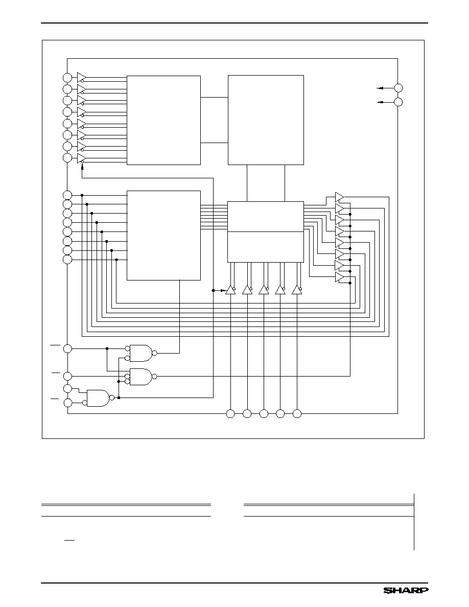
MEMORY
ARRAY
(256 x 256)
13
17
12
16
A
6
WE
A
7
A
12
27
A
8
COLUMN I/O
CIRCUITS
COLUMN SELECT
V
CC
GND
OE
I/O
7
I/O
6
I/O
5
I/O
4
I/O
3
I/O
2
I/O
1
22
19
8
A
2
A
1
A
0
A
11
23
9
10
28
14
A
9
CE
1
20
26
CE
2
INPUT
DATA
CONTROL
A
10
21
ROW
SELECT
5
6
7
4
3
2
25
24
NOTE: Pin numbers apply to the 28-pin SOP.
Figure 3. LH5164AV Block Diagram
PIN DESCRIPTION
SIGNAL
PIN NAME
A
0
- A
12
Address inputs
CE
1
/CE
2
Chip Enable input
WE
Write Enable input
OE
Output Enable input
SIGNAL
PIN NAME
I/O
1
- I/O
8
Data inputs and outputs
V
CC
Power supply
GND
Ground
NC
No connection
LH5164AV
CMOS 64K (8K
◊
8) Static RAM
2
TRUTH TABLE
CE
1
CE
2
WE
OE
MODE
I/O
1
- I/O
8
SUPPLY CURRENT
NOTE
H
X
X
X
Standby
High-Z
Standby (I
SB
)
1
X
L
X
X
L
H
L
X
Write
Data input
Operating (I
CC
)
1
L
H
H
L
Read
Data output
Operating (I
CC
)
L
H
H
H
Output disable
High-Z
Operating (I
CC
)
NOTE:
1.
X = H or L
ABSOLUTE MAXIMUM RATINGS
PARAMETER
SYMBOL
RATING
UNIT
NOTE
Supply voltage
V
CC
≠0.3 to +7.0
V
1
Input voltage
V
IN
≠0.3 to V
CC
+0.3
V
1, 2
Operating temperature
Topr
≠10 to +70
∞
C
Storage temperature
Tstg
≠65 to +150
∞
C
NOTES:
1.
The maximum applicable voltage on any pin with respect to GND.
2.
V
IN
(MIN.) = ≠3.0 V for pulse width
50 ns.
RECOMMENDED OPERATING CONDITIONS (T
A
= ≠10
∞
C to +70
∞
C)
PARAMETER
SYMBOL
MIN.
TYP.
MAX.
UNIT
NOTE
Supply voltage
V
CC
2.7
5.5
V
Input voltage
(V
CC
= 2.7 V to 3.6 V)
V
IH
V
CC
≠ 0.5
V
CC
+ 0.3
V
V
IL
≠0.3
0.2
V
1
Input voltage
(V
CC
= 4.5 V to 5.5 V)
V
IH
2.2
V
CC
+ 0.3
V
V
IL
≠0.3
0.8
V
1
NOTE:
1.
V
IL
(MIN.) = ≠3.0 V for pulse width
50 ns.
CMOS 64K (8K
◊
8) Static RAM
LH5164AV
3
DC CHARACTERISTICS
1
(T
A
= ≠10
∞
C to +70
∞
C, V
CC
= 2.7 V to 5.5 V)
PARAMETER
SYMBOL
CONDITIONS
MIN.
MAX.
UNIT
NOTE
Input leakage
current
I
LI
V
IN
= 0 V to V
CC
≠1.0
1.0
µ
A
Output leakage
current
I
LO
CE
1
= V
IH
or CE
2
= V
IL
or
OE = V
IH
or WE = V
IL
V
I/O
= 0 to V
CC
≠1.0
1.0
µ
A
Operating supply
current
I
CC
CE
1
= 0.2 V, V
IN
= 0.2 V, or
V
CC
≠ 0.2 V
CE
2
= V
CC
≠ 0.2 V,
Outputs open,
V
CC
= 2.7 V to 3.6 V
t
CYCLE
=
200 ns
20
mA
t
CYCLE
=
1.0
µ
s
8
CE
1
= V
IL
, V
IN
= V
IL
or V
IH
CE
2
= V
IH
, Outputs open,
V
CC
= 4.5 V to 5.5 V
t
CYCLE
=
200 ns
45
t
CYCLE
=
1.0
µ
s
10
Standby current
I
SB
CE
2
0.2 V or
CE
1
V
CC
≠ 0.2 V
V
CC
= 2.7 V
to 3.6 V
0.6
µ
A
1
V
CC
= 4.5 V
to 5.5 V
1.0
I
SB1
CE
1
= V
IH
or
CE
2
= V
IL
5
mA
Output voltage
V
OL
I
OL
= 500
µ
A, V
CC
= 2.7 V to 3.6 V
0.4
V
I
OL
= 2.1 mA, V
CC
= 4.5 V to 5.5 V
0.4
V
OH
I
OH
= ≠500
µ
A, V
CC
= 2.7 V to 3.6 V
V
CC
≠
0.5
V
I
OH
= ≠1.0 mA, V
CC
= 4.5 V to 5.5 V
2.4
NOTE:
1.
CE
2
should be
V
CC
≠ 0.2 V or
0.2 V when CE
1
V
CC
≠ 0.2 V.
LH5164AV
CMOS 64K (8K
◊
8) Static RAM
4
READ CYCLE (T
A
= ≠10
∞
C to +70
∞
C, V
CC
= 2.7 V to 5.5 V)
PARAMETER
SYMBOL
MIN.
MAX.
UNIT
Read cycle time
t
RC
200
ns
Address access time
t
AA
200
ns
CE
1
access time
t
ACE1
200
ns
CE
2
access time
t
ACE2
200
ns
Output enable access time
t
OE
150
ns
Output hold time
t
OH
10
ns
CE
1
Low to output in Low-Z
t
LZ1
20
ns
CE
2
High to output in Low-Z
t
LZ2
20
ns
OE Low to output in Low-Z
t
OLZ
10
ns
CE
1
High to output in High-Z
t
HZ1
0
60
ns
CE
2
Low to output in High-Z
t
HZ2
0
60
ns
OE High to output in High-Z
t
OHZ
0
40
ns
WRITE CYCLE (T
A
= ≠10
∞
C to +70
∞
C, V
CC
= 2.7 V to 5.5 V)
PARAMETER
SYMBOL
MIN.
MAX.
UNIT
Write cycle time
t
WC
200
ns
CE Low to end of write
t
CW
180
ns
Address valid to end of write
t
AW
180
ns
Address setup time
t
AS
0
ns
Write pulse width
t
WP
150
ns
Write recovery time
t
WR
0
ns
Input data setup time
t
DW
100
ns
Input data hold time
t
DH
0
ns
WE High to output in Low-Z
t
OW
20
ns
WE Low to output in High-Z
t
WZ
0
60
ns
OE High to output in High-Z
t
OHZ
0
40
ns
TEST CONDITIONS
PARAMETER
MODE
NOTE
Input pulse level
0.2 V to V
CC
≠ 0.2 V
Input rise/fall time
10 ns
Input/output timing level
1.5 V
Output load
C
L
(100 pF)
1
NOTE:
1.
Includes scope and jig capacitance.
CAPACITANCE
1
(T
A
= 25
∞
C, f = 1 MHz)
PARAMETER
SYMBOL
CONDITIONS
MIN.
TYP.
MAX.
UNIT
Input capacitance
C
IN
V
IN
= 0 V
7
pF
I/O capacitance
C
I/O
V
I/O
= 0 V
10
pF
NOTE:
1.
This parameter is sampled and not production tested.
CMOS 64K (8K
◊
8) Static RAM
LH5164AV
5
DATA RETENTION CHARACTERISTICS (T
A
= ≠10
∞
C to +70
∞
C)
PARAMETER
SYMBOL
CONDITIONS
MIN.
MAX.
UNIT
NOTE
Data retention supply voltage
V
CCDR
CE
2
0.2 V or
CE
1
V
CCDR
≠ 0.2 V
2.0
5.5
V
1
Data retention supply current
I
CCDR
V
CCDR
= 3 V,
CE
2
0.2 V or
CE
1
V
CCDR
≠ 0.2 V
T
A
=
25
∞
C
0.2
µ
A
1
T
A
=
40
∞
C
0.4
µ
A
0.6
µ
A
Chip disable to data retention
t
CDR
0
ns
Recovery time
t
R
t
RC
ns
2
NOTES:
1.
CE
2
should be
V
CCDR
≠ 0.2 V or
0.2 V when CE
1
V
CCDR
≠ 0.2 V.
2.
t
RC
= Read cycle time.
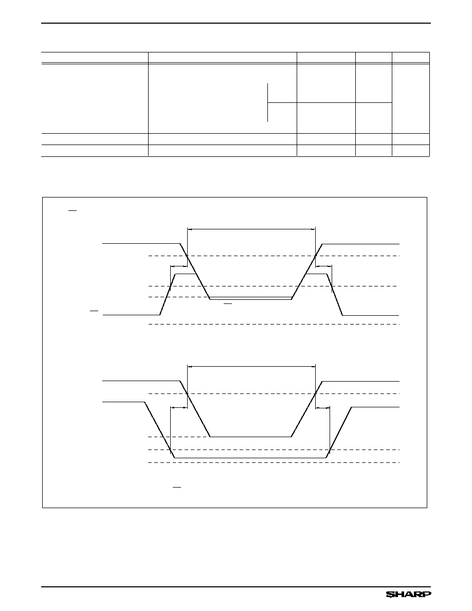
DATA RETENTION MODE
V
CC
0 V
t
CDR
5164AV-7
t
R
V
CCDR
CE
1
CE
1
V
CCDR
- 0.2 V
CE
2
CONTROL
CE
1
CONTROL (NOTE)
NOTE: To control the data retention mode at CE
1
, fix the input level of CE
2
between
V
CCDR
to V
CCDR
- 0.2 V or 0 V and 0.2 V during the data retention mode.
- 0.5 V
2.7 V
V
CC
DATA RETENTION MODE
V
CC
0 V
t
CDR
t
R
V
CCDR
CE
2
CE
2
0.2 V
2.7 V
0.2 V
Figure 4. Data Retention Characteristics
LH5164AV
CMOS 64K (8K
◊
8) Static RAM
6
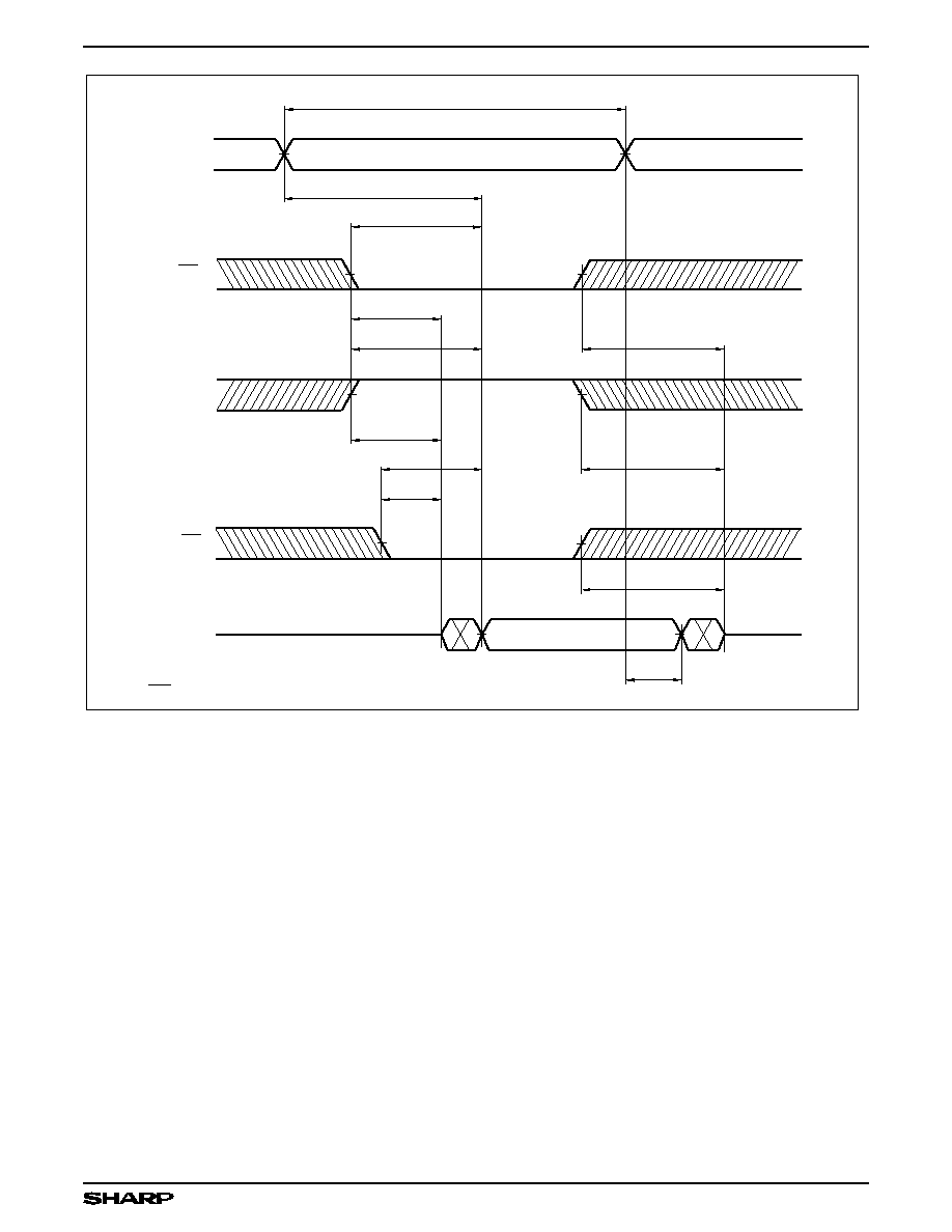
t
LZ1
t
ACE1
A
0
- A
12
t
OHZ
D
OUT
DATA VALID
OE
t
RC
5164AV-4
t
OLZ
NOTE: WE = 'HIGH.'
t
ACE2
t
AA
t
LZ2
CE
1
CE
2
t
HZ1
t
OE
t
OH
t
HZ2
Figure 5. Read Cycle
CMOS 64K (8K
◊
8) Static RAM
LH5164AV
7
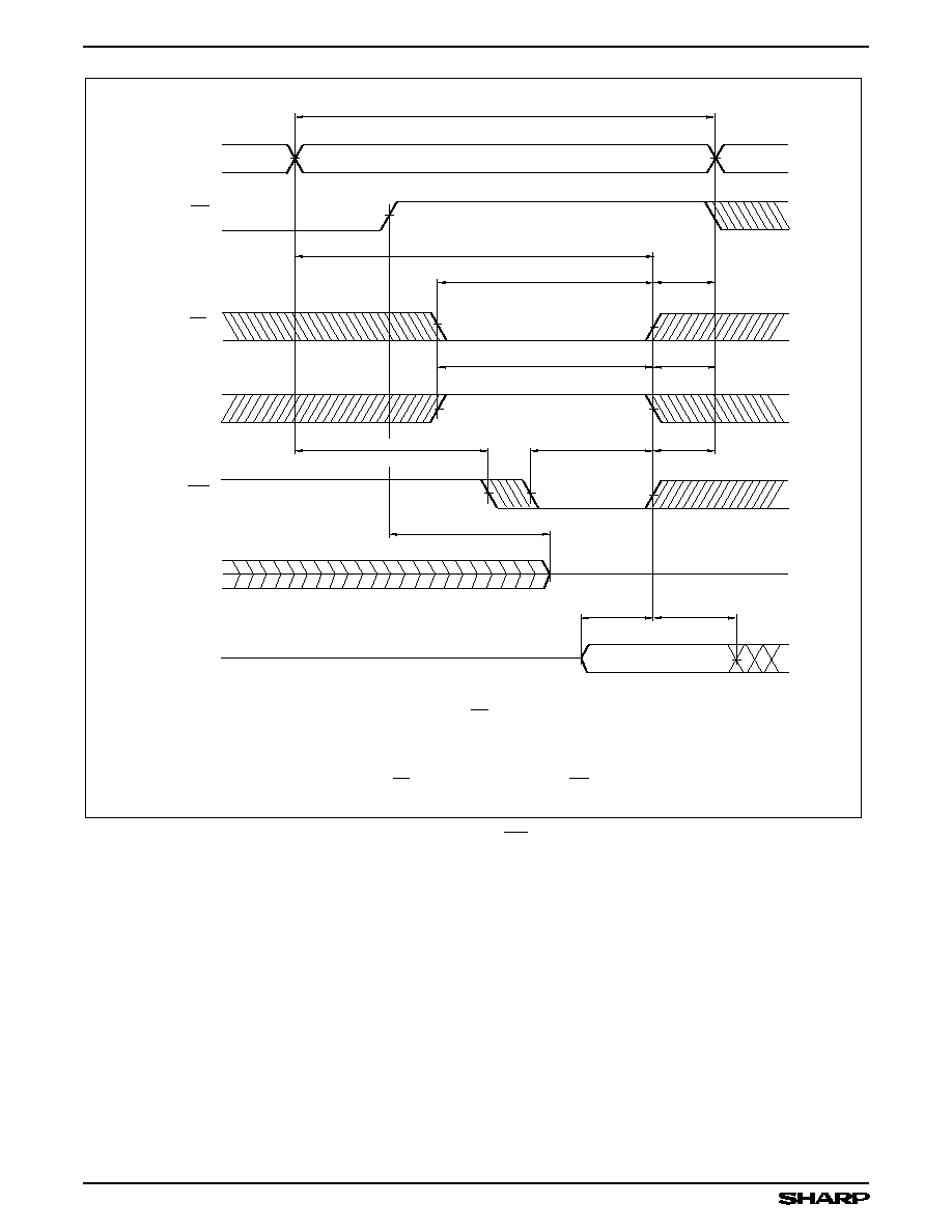
DATA VALID
t
DH
t
DW
WE
D
IN
t
CW
OE
t
WC
5164AV-5
t
WR
t
CW
t
AW
CE
1
CE
2
t
AS
t
OHZ
t
WP
t
WR
D
OUT
t
WR
(NOTE 2)
(NOTE 1)
(NOTE 3)
(NOTE 4)
(NOTE 5)
NOTES:
1. t
CW
is defined as the time from the last occuring transition, either CE
1
LOW transition or CE
2
HIGH transition, to the time when the writing is finished.
2. t
WR
is defined as the time from writing finish to address change.
3. t
AS
is defined as the time from address change to writing start.
4. The writing occurs during an overlapping period of CE
1
= 'LOW,' CE
2
= 'HIGH,' and WE = 'LOW' (t
WP
).
5. When I/O pins are in the output state, input signals with the opposite logic level must not be applied.
A
0
- A
12
Figure 6. Write Cycle (OE Controlled)
LH5164AV
CMOS 64K (8K
◊
8) Static RAM
8
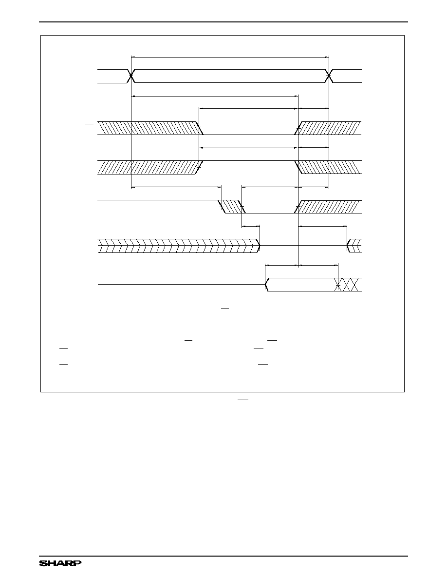
DATA VALID
t
DH
t
DW
WE
D
IN
t
CW
t
WC
t
CW
t
AW
CE
1
CE
2
t
AS
t
WP
D
OUT
t
WZ
t
WR
t
OW
t
WR
t
WR
5164AV-6
(NOTE 4)
(NOTE 1)
(NOTE 3)
(NOTE 2)
(NOTE 7)
(NOTE 5)
(NOTE 6)
NOTES:
1. t
CW
is defined as the time from the last occuring transition, either CE
1
LOW transition or CE
2
HIGH transition,
to the time when the writing is finished.
2. t
WR
is defined as the time from writing finish to address change.
3. t
AS
is defined as the time from address change to writing start.
4. The writing occurs during an overlapping period of CE
1
= 'LOW,' CE
2
= 'HIGH,' and WE = 'LOW' (t
WP
).
5. If CE
1
LOW transition or CE
2
HIGH transition occurs at the same time or after WE LOW transition, the
outputs will remain high-impedance.
6. If CE
1
HIGH transition or CE
2
LOW transition occurs at the same time or before WE HIGH transition,
the outputs will remain high-impedance.
7. When I/O pins are in the output state, input signals with the opposite logic level must not be applied.
A
0
- A
12
Figure 7. Write Cycle (OE Low Fixed)
CMOS 64K (8K
◊
8) Static RAM
LH5164AV
9
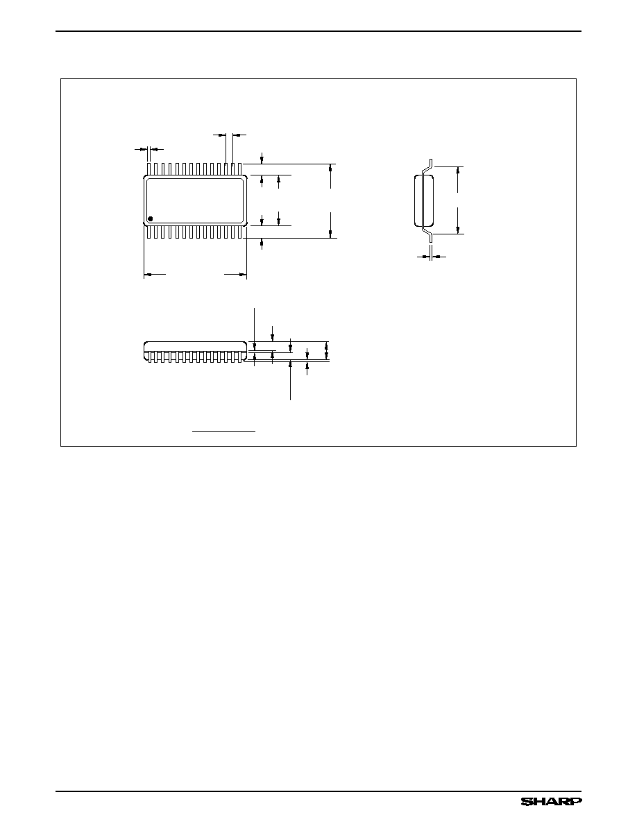
DIMENSIONS IN MM [INCHES]
MAXIMUM LIMIT
MINIMUM LIMIT
28SOP (SOP028-P-0450)
12.40 [0.488]
11.60 [0.457]
8.80 [0.346]
8.40 [0.331]
10.60 [0.417]
18.20 [0.717]
17.80 [0.701]
0.15 [0.006]
1.025 [0.040]
0.20 [0.008]
0.00 [0.000]
1.025 [0.040]
2.40 [0.094]
2.00 [0.079]
0.20 [0.008]
0.10 [0.004]
0.50 [0.020]
0.30 [0.012]
1.27 [0.050]
TYP.
28
15
14
1
1.70 [0.067]
1.70 [0.067]
28SOP
28-pin, 450-mil SOP
PACKAGE DIAGRAMS
LH5164AV
CMOS 64K (8K
◊
8) Static RAM
10
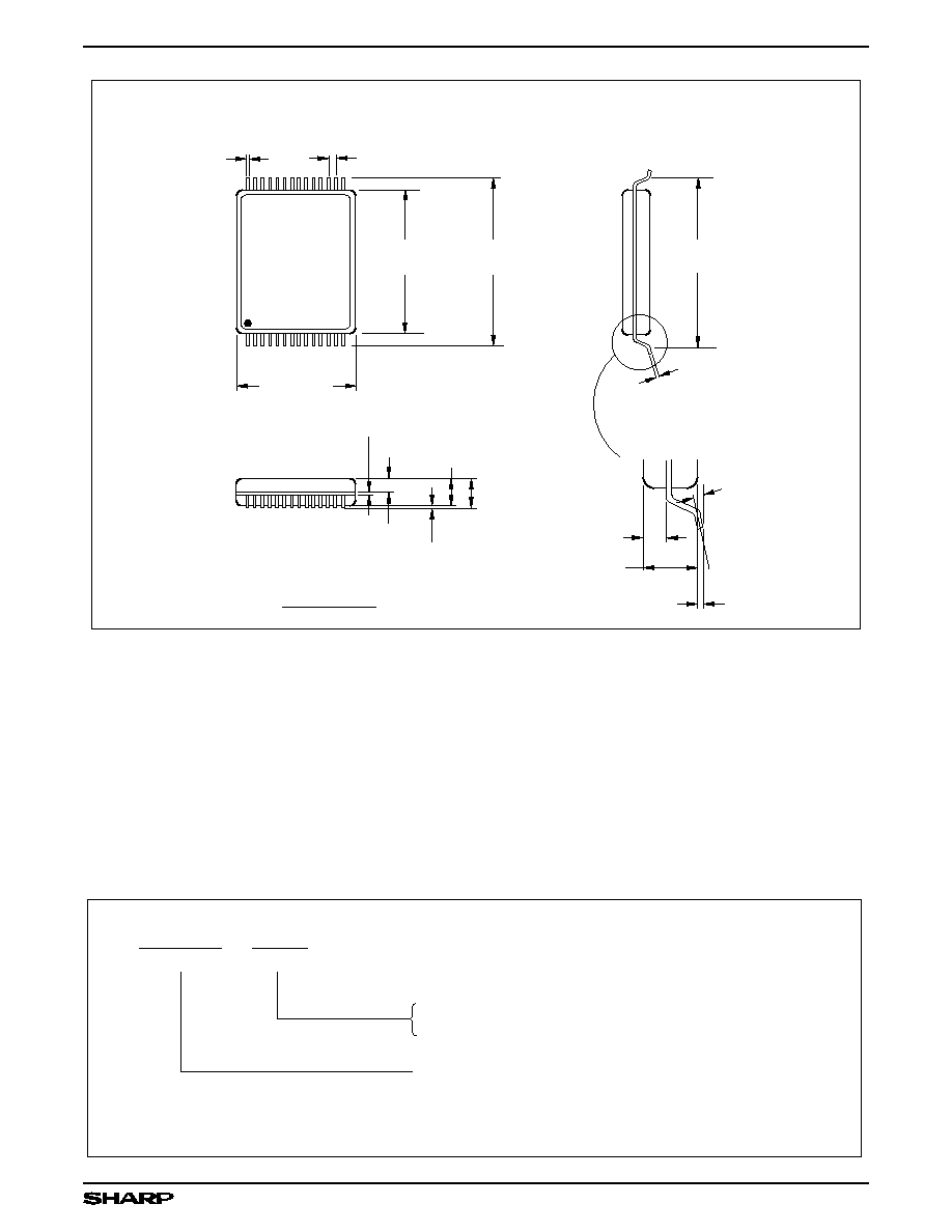
DIMENSIONS IN MM [INCHES]
MAXIMUM LIMIT
MINIMUM LIMIT
28TSOP (TSOP028-P-0813)
28
1
28TSOP
14
15
0.28 [0.011]
0.12 [0.005]
0.55 [0.022]
TYP.
12.00 [0.472]
11.60 [0.457]
13.70 [0.539]
13.10 [0.516]
8.20 [0.323]
7.80 [0.307]
0.15 [0.006]
1.10 [0.043]
0.90 [0.035]
1.20 [0.047]
MAX.
12.60 [0.496]
12.20 [0.480]
0.20 [0.008]
0.10 [0.004]
0.20 [0.008]
0.00 [0.000]
1.10 [0.043]
0.90 [0.035]
0.425 [0.017]
0.20 [0.008]
0.00 [0.000]
0 - 10
∞
DETAIL
0.425 [0.017]
28-pin, 8
◊
13 mm
2
TSOP (Type I)
LH5164AV
Device Type
X
Package
5164AV-8
CMOS 64K (8K x 8) Static RAM
N 28-pin, 450-mil SOP (SOP028-P-0450)
T 28-pin, 8 x 13 mm
2
TSOP (Type I) (TSOP028-P-0813)
Example: LH5164AVN (CMOS 64K (8K x 8) Static RAM, 28-pin, 450-mil SOP)
ORDERING INFORMATION
CMOS 64K (8K
◊
8) Static RAM
LH5164AV
11