LH52256C/CH
CMOS 256K (32K
◊
8) Static RAM
FEATURES
∑∑
32,768
◊
8 bit organization
∑∑
Access time: 70 ns (MAX.)
∑∑
Supply current:
Operating: 45 mA (MAX.)
10 mA (MAX.) (t
RC
, t
WC
= 1
µ
s)
Standby: 40
µ
A (MAX.)
∑∑
Data retention current: 1.0
µ
A (MAX.)
(V
CCDR
= 3 V, T
A
= 25
∞
C)
∑∑
Wide operating voltage range:
4.5 V
±
5.5 V
∑∑
Operating temperature:
Commerical temperature 0
∞
C to +70
∞
C
Industrial temperature -40∞ to +85∞C
∑∑
Fully-static operation
∑∑
Three-state outputs
∑∑
Not designed or rated as radiation
hardened
∑∑
Package:
28-pin, 600-mil DIP
28-pin, 450-mil SOP
28-pin, 300-mil SK-DIP
28-pin, 8
◊
3 mm
2
TSOP (Type I)
∑∑
N-type bulk silicon
DESCRIPTION
The LH52256C is a Static RAM organized as
32,768
◊
8 bits which provides low-power standby
mode. It is fabricated using silicon-gate CMOS process
technology.
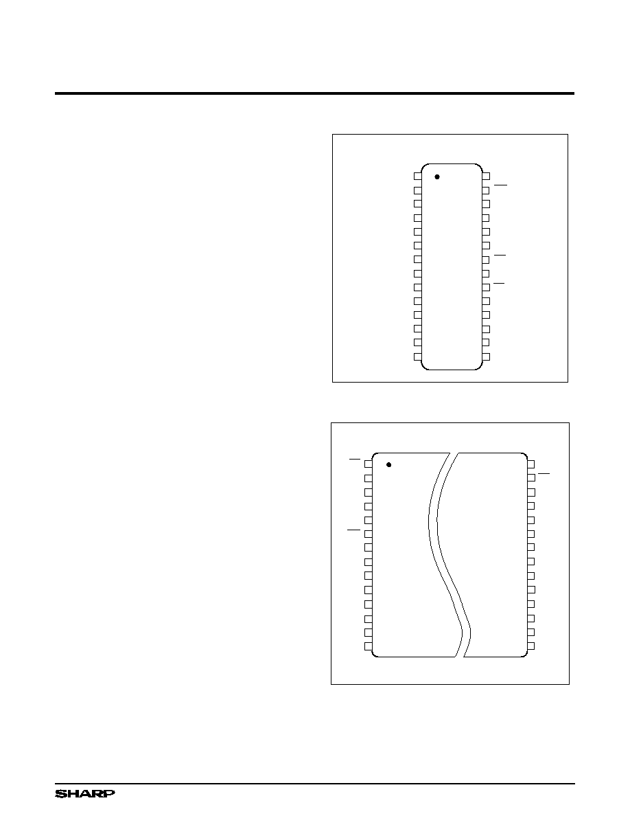
PIN CONNECTIONS
52256C-1
1
2
3
4
5
6
7
8
9
10
11
12
13
14
A
14
A
12
A
7
A
6
A
5
A
4
A
3
A
2
A
1
A
0
28
27
26
25
24
23
22
21
20
19
18
17
16
15
V
CC
WE
A
9
A
11
OE
A
10
I/O
6
I/O
5
GND
I/O
8
I/O
7
CE
A
13
A
8
I/O
1
I/O
2
I/O
3
I/O
4
28-PIN DIP
28-PIN SK-DIP
28-PIN SOP
TOP VIEW
Figure 1. Pin Connections
2
3
4
5
6
9
10
7
8
A
11
11
1
28
27
26
25
22
21
24
23
20
19
A
10
28-PIN TSOP (Type I)
12
13
14
17
16
18
15
OE
A
8
A
9
A
13
WE
A
12
A
14
I/O
3
I/O
2
A
1
I/O
8
CE
I/O
6
I/O
7
GND
I/O
5
I/O
4
I/O
1
A
0
52256C-8
V
CC
A
7
A
6
A
5
A
4
A
3
A
2
NOTE: Reverse bend available on request.
Figure 2. TSOP (Type I) Pin Connections
1
A
4
A
3
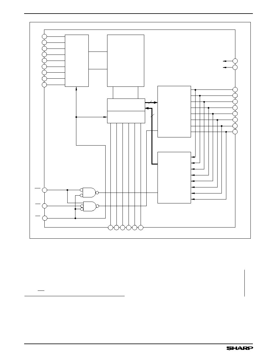
52256C-2
MEMORY
ARRAY
(512 x 512)
A
5
ROW
DECORDER
WE
A
6
A
7
27
A
12
V
CC
GND
OE 22
28
14
A
13
CE 20
COLUMN I/O
CIRCUIT
COLUMN
DECODER
OUTPUT
BUFFERS
I/O
1
11
12
13
15
16
17
18
19
I/O
2
I/O
3
I/O
4
I/O
5
I/O
6
I/O
7
I/O
8
10 9
8
21 24 23
INPUT
DATA
CONTROL
26
2
3
4
5
6
7
A
0
A
1
A
2
A
10
A
9
A
11
A
14
A
8
25
1
8
8
Figure 3. LH52256C Block Diagram
PIN DESCRIPTION
SIGNAL
PIN NAME
A
0
- A
14
Address inputs
CE
Chip enable
WE
Write enable
OE
Output enable
SIGNAL
PIN NAME
I/O
1
- I/O
8
Data inputs and outputs
V
CC
Power supply
GND
Ground
LH52256C/CH
CMOS 256K (32K
◊
8) Static RAM
2
TRUTH TABLE
CE
WE
OE
MODE
I/O
1
- I/O
8
SUPPLY CURRENT
NOTE
H
X
X
Standby
High impedance
Standby (I
SB
)
1
L
H
L
Read
Data output
Active (I
CC
)
1
L
H
H
Output disable
High impedance
Active (I
CC
)
1
L
L
X
Write
Data input
Active (I
CC
)
1
NOTE:
1.
X = Don't care, L = Low, H = High
ABSOLUTE MAXIMUM RATINGS
PARAMETER
SYMBOL
RATING
UNIT
NOTE
Supply voltage
V
CC
≠0.5 to +7.0
V
1
Input voltage
V
IN
≠0.5 to V
CC
+ 0.5
V
1, 2
Operating temperature
T
OPR
0 to +70
∞
C
Storage temperature
T
STG
≠65 to +150
∞
C
NOTES:
1.
The maximum applicable voltage on any pin with respect to GND.
2.
Undershoot of -3.0 V is allowed width of pulse below 50 ns.
RECOMMENDED DC OPERATING CONDITIONS (T
A
= 0
∞
C to +70
∞
C)
PARAMETER
SYMBOL
MIN.
TYP.
MAX.
UNIT
NOTE
Supply voltage
V
CC
4.5
5.0
5.5
V
Input voltage
V
IH
2.2
V
CC
+ 0.5
V
V
IL
≠0.5
0.8
V
1
NOTE:
1.
Undershoot of -3.0 V is allowed width of pulse below 50 ns.
CMOS 256K (32K
◊
8) Static RAM
LH52256C/CH
3

DC ELECTRICAL CHARACTERISTICS (T
A
= 0
∞
C to +70
∞
C, V
CC
= 4.5 V to 5.5 V)
PARAMETER
SYMBOL
CONDITIONS
MIN.
TYP.
MAX.
UNIT
Input leakage
current
I
LI
V
IN
= 0 V to V
CC
≠1.0
1.0
µ
A
Output leakage
current
I
LO
CE = V
IH
or OE = V
IH
V
I/O
= 0 V to V
CC
≠1.0
1.0
µ
A
Operating supply
current
I
CC
Minimum cycle, V
IN
= V
IL
or V
IH
I
I/O
= 0 mA, CE = V
IL
25
45.0
mA
I
CC1
t
RC
, t
WC
= 1
µ
s, V
IN
= V
IL
or V
IH
,
I
I/O
= 0 mA, CE = V
IL
10.0
Standby current
I
SB
CE
V
CC
≠ 0.2 V
0.6
40.0
µ
A
I
SB1
CE = V
IH
3.0
mA
Output voltage
V
OL
I
OL
= 2.1 mA
0.4
V
V
OH
I
OH
= -1.0 mA
2.4
NOTE:
Typical values at V
CC
= 5.0 V, T
A
= 25
∞
C
AC ELECTRICAL CHARACTERISTICS
AC Test Conditions
PARAMETER
MODE
NOTE
Input pulse level
0.6 V to 2.4 V
Input rise and fall time
10 ns
Input and output timing Ref. level
1.5 V
Output load
1 TTL + C
L
(100 pF)
1
NOTE:
1.
Including scope and jig capacitance.
READ CYCLE (T
A
= 0
∞
C to +70
∞
C, V
CC
= 4.5 V to 5.5 V)
PARAMETER
SYMBOL
MIN.
MAX.
UNIT
NOTE
Read cycle time
t
RC
70
ns
Address access time
t
AA
70
ns
CE access time
t
ACE
70
ns
Output enable to output valid
t
OE
35
ns
Output hold from address change
t
OH
10
ns
CE Low to output active
t
LZ
10
ns
1
OE Low to output active
t
OLZ
5
ns
1
CE High to output in High impedance
t
HZ
0
30
ns
1
OE High to output in High impedance
t
OHZ
0
30
ns
1
NOTES:
1.
Active output to high-impedance and high-impedance to output active tests specified for a
±
200 mV
transition from steady state levels into the test load.
LH52256C/CH
CMOS 256K (32K
◊
8) Static RAM
4

WRITE CYCLE (T
A
= 0
∞
C to +70
∞
C, V
CC
= 4.5 V to 5.5 V)
PARAMETER
SYMBOL
MIN.
MAX.
UNIT
NOTE
Write cycle time
t
WC
70
ns
CE Low to end of write
t
CW
45
ns
Address valid to end of write
t
AW
45
ns
Address setup time
t
AS
0
ns
Write pulse width
t
WP
35
ns
Write recovery time
t
WR
0
ns
Input data setup time
t
DW
30
ns
Input data hold time
t
DH
0
ns
WE High to output active
t
OW
5
ns
1
WE Low to output in High
impedance
t
WZ
0
30
ns
1
OE High to output in High
impedance
t
OHZ
0
30
ns
1
NOTE:
1.
Active output to high-impedance and high-impedance to output active tests specified for a
±
200 mV
transition from steady state levels into the test load.
CAPACITANCE (T
A
= 25
∞
C, f = 1MHz)
PARAMETER
SYMBOL
CONDITIONS
MIN.
TYP.
MAX.
UNIT
NOTE
Input capacitance
C
IN
V
IN
= 0 V
7
pF
1
I/O capacitance
C
I/O
V
I/O
= 0 V
10
pF
1
NOTE:
1.
This parameter is sampled and not production tested.
DATA RETENTION CHARACTERISTICS (T
A
= 0
∞
C to +70
∞
C)
PARAMETER
SYMBOL
CONDITIONS
MIN.
TYP.
MAX.
UNIT
NOTE
Data retention supply voltage
V
CCDR
CE
V
CCDR
≠ 0.2 V
2.0
5.5
V
Data retention supply current
I
CCDR
V
CCDR
= 3.0 V
CE
V
CCDR
≠ 0.2 V
T
A
= 25
∞
C
0.3
1.0
µ
A
TA = 40
∞
C
3.0
15
Chip enable setup time
t
CDR
0
ns
Chip enable hold time
t
R
t
RC
ns
1
NOTE:
1.
t
RC
= Read cycle time.
2.
Typical values at T
A
= 25
∞
C
CMOS 256K (32K
◊
8) Static RAM
LH52256C/CH
5

D
OUT
DATA VALID
t
RC
t
AA
t
ACE
t
LZ
t
OLZ
t
OH
t
OHZ
t
HZ
52256C-3
ADDRESS
t
OE
OE
CE
NOTE: WE is HIGH for Read Cycle.
Figure 4. Read Cycle
LH52256C/CH
CMOS 256K (32K
◊
8) Static RAM
6

D
IN
52256C-4
ADDRESS
OE
t
WC
t
AW
t
WR
t
CW
t
AS
t
WP
t
OHZ
t
DW
t
WR
t
DH
DATA VALID
CE
WE
D
OUT
1. A write occurs during the overlap of a LOW CE, and a LOW WE.
A write begins at the latest transition among CE going LOW, and
WE going LOW. A write ends at the earliest transition among CE
going HIGH, and WE going HIGH. t
WP
is measured from the beginning
of write to the end of write.
2. t
CW
is measured from the later of CE going LOW to the end of write.
3. t
AS
is measured from the address valid to the beginning of write.
4. t
WR
is measured from the end of write to the address change.
5. During this period, I/O pins are in the output state, therefore the input
signals of opposite phase to the outputs must not be applied.
6. If CE goes LOW simultaneously with WE going LOW or after WE going
LOW, the outputs remain in high impedance state.
7. If CE goes HIGH simulaneously with WE going HIGH or before WE
going HIGH, the outputs remain in high impedance state.
NOTES:
(NOTE 4)
(NOTE 2)
(NOTE 1)
(NOTE 3)
(NOTE 6)
(NOTE 5)
(NOTE 4)
Figure 5. Write Cycle (OE Controlled)
CMOS 256K (32K
◊
8) Static RAM
LH52256C/CH
7

DATA VALID
t
DH
t
DW
WE
D
IN
t
CW
ADDRESS
t
WC
52256C-5
t
WR
t
AW
CE
t
AS
t
WZ
t
WP
(NOTE 2
)
(NOTE 4)
(NOTE 3)
D
OUT
(NOTE 6)
(NOTE 1)
t
WR
t
OW
(NOTE 7)
(NOTE 5)
(NOTE 4)
1. A write occurs during the overlap of a LOW CE, and a LOW WE.
A write begins at the latest transition among CE going LOW, and
WE going LOW. A write ends at the earliest transition among CE
going HIGH, and WE going HIGH. t
WP
is measured from the beginning
of write to the end of write.
2. t
CW
is measured from the later of CE going LOW to the end of write.
3. t
AS
is measured from the address valid to the beginning of write.
4. t
WR
is measured from the end of write to the address change.
5. During this period, I/O pins are in the output state, therefore the input
signals of opposite phase to the outputs must not be applied.
6. If CE goes LOW simultaneously with WE going LOW or after WE going
LOW, the outputs remain in high impedance state.
7. If CE goes HIGH simulaneously with WE going HIGH or before WE
going HIGH, the outputs remain in high impedance state.
NOTES:
Figure 6. Write Cycle (OE Low Fixed)
t
CDR
V
CC
4.5 V
2.2 V
V
CCDR
0 V
CE
CE
V
CCDR
- 0.2 V
DATA RETENTION MODE
t
R
52256C-6
CE
CONTROL
Data Retention Timing Chart
CE Controlled
LH52256C/CH
CMOS 256K (32K
◊
8) Static RAM
8
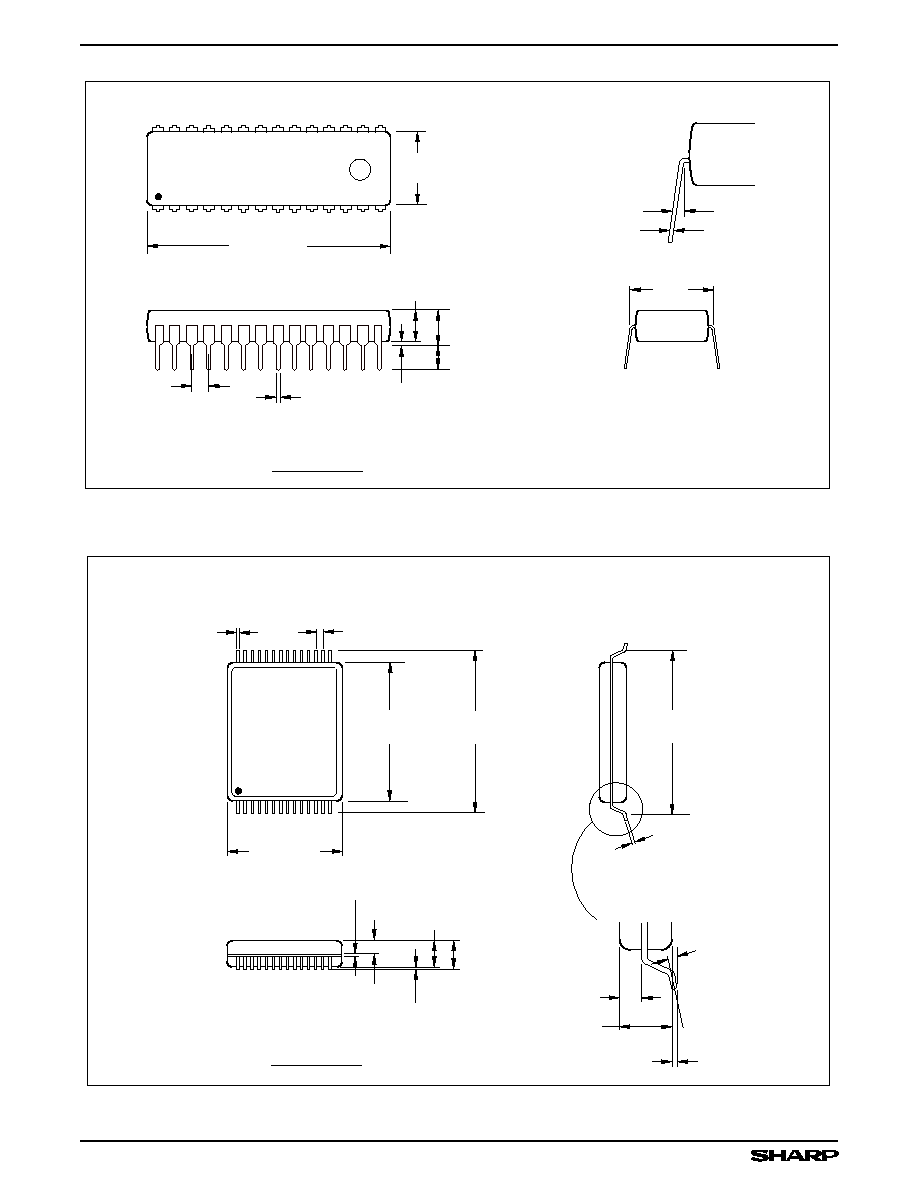
PACKAGE DIAGRAMS
DIMENSIONS IN MM [INCHES]
MAXIMUM LIMIT
MINIMUM LIMIT
28DIP (DIP028-P-0600)
1
14
15
28
28DIP-2
13.45 [0.530]
12.95 [0.510]
0.51 [0.020] MIN.
5.20 [0.205]
5.00 [0.197]
3.50 [0.138]
3.00 [0.118]
2.54 [0.100]
TYP.
0.60 [0.024]
0.40 [0.016]
0.30 [0.012]
0.20 [0.008]
DETAIL
36.30 [1.429]
35.70 [1.406]
0
∞
TO 15
∞
4.50 [0.177]
4.00 [0.157]
15.24 [0.600]
TYP.
DIMENSIONS IN MM [INCHES]
MAXIMUM LIMIT
MINIMUM LIMIT
28SOP (SOP028-P-0450)
12.40 [0.488]
11.60 [0.457]
8.80 [0.346]
8.40 [0.331]
10.60 [0.417]
18.20 [0.717]
17.80 [0.701]
0.15 [0.006]
1.025 [0.040]
0.20 [0.008]
0.00 [0.000]
1.025 [0.040]
2.40 [0.094]
2.00 [0.079]
0.20 [0.008]
0.10 [0.004]
0.50 [0.020]
0.30 [0.012]
1.27 [0.050]
TYP.
28
15
14
1
1.70 [0.067]
1.70 [0.067]
28SOP
CMOS 256K (32K
◊
8) Static RAM
LH52256C/CH
9
0.51 [0.020] MIN
4.60 [0.181]
4.20 [0.205]
3.50 [0.138]
3.00 [0.118]
1.78 [0.070]
TYP.
0.56 [0.022]
0.36 [0.014]
0.30 [0.012]
0.20 [0.008]
DETAIL
25.75 [1.014]
25.25 [0.994]
0
∞
TO 15
∞
4.05 [0.159]
3.65 [0.144]
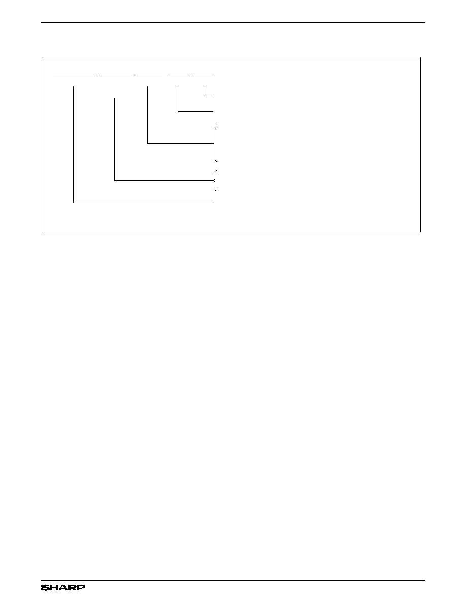
28SDIP (SDIP28-P-400)
DIMENSIONS IN MM [INCHES]
MAXIMUM LIMIT
MINIMUM LIMIT
8.80 [0.346]
8.40 [0.331]
14
15
1
28
10.16 [0.400]
TYP.
28SDIP
DIMENSIONS IN MM [INCHES]
MAXIMUM LIMIT
MINIMUM LIMIT
28TSOP (TSOP028-P-0813)
28
1
28TSOP
14
15
0.28 [0.011]
0.12 [0.005]
0.55 [0.022]
TYP.
12.00 [0.472]
11.60 [0.457]
13.70 [0.539]
13.10 [0.516]
8.20 [0.323]
7.80 [0.307]
0.15 [0.006]
1.10 [0.043]
0.90 [0.035]
1.20 [0.047]
MAX.
12.60 [0.496]
12.20 [0.480]
0.20 [0.008]
0.10 [0.004]
0.20 [0.008]
0.00 [0.000]
1.10 [0.043]
0.90 [0.035]
0.425 [0.017]
0.20 [0.008]
0.00 [0.000]
0 - 10
∞
DETAIL
0.425 [0.017]
LH52256C/CH
CMOS 256K (32K
◊
8) Static RAM
10
Low-Low-power standby
LH52256C
Device Type
X
Package
- ##
Speed
52256C-7
CMOS 32K x 8 Static RAM
Example: LH52256C-70LL (CMOS 32K x 8 Static RAM, Low-Low-power standby, 70 ns, 28-pin, 600-mil DIP)
70 Access Time (ns)
LL
Power
Blank 28-pin, 600-mil DIP (DIP028-P-0600)
D 28-pin, 300-mil SK-DIP (DIP028-P-0300)
N 28-pin, 450-mil SOP (SOP028-P-0450)
T 28-pin, 8 x 13 mm
2
TSOP (Type I) (TSOP028-P-0813)
X
Operating
Temp
Blank 0
∞
to +70
∞
C
H -4
∞
to +85
∞
C
ORDERING INFORMATION
CMOS 256K (32K
◊
8) Static RAM
LH52256C/CH
11

NORTH AMERICA
EUROPE
ASIA
SHARP Microelectronics
of the Americas
5700 NW Pacific Rim Blvd.
Camas, WA 98607, U.S.A.
Phone: (360) 834-2500
Fax: (360) 834-8903
http://www.sharpsma.com
SHARP Microelectronics Europe
Sonninstraþe 3
20097 Hamburg, Germany
Phone: (49) 40 2376-2286
Fax: (49) 40 2376-2232
http://www.sharpsme.com
SPECIFICATIONS ARE SUBJECT TO CHANGE WITHOUT NOTICE.
Suggested applications (if any) are for standard use; See Important Restrictions for limitations on special applications. See Limited Warranty
for SHARP's product warranty. The Limited Warranty is in lieu, and exclusive of, all other warranties, express or implied. ALL EXPRESS
AND IMPLIED WARRANTIES, INCLUDING THE WARRANTIES OF MERCHANTABILITY, FITNESS FOR USE AND FITNESS FOR A
PARTICULAR PURPOSE, ARE SPECIFICALLY EXCLUDED. In no event will SHARP be liable, or in any way responsible, for any incidental
or consequential economic or property damage.
SHARP Corporation
Integrated Circuits Group
2613-1 Ichinomoto-Cho
Tenri-City, Nara, 632, Japan
Phone: +81-743-65-1321
Fax: +81-743-65-1532
http://www.sharp.co.jp