 | –≠–ª–µ–∫—Ç—Ä–æ–Ω–Ω—ã–π –∫–æ–º–ø–æ–Ω–µ–Ω—Ç: LH52258A | –°–∫–∞—á–∞—Ç—å:  PDF PDF  ZIP ZIP |
LH52258A
CMOS 32K
◊
8 Static RAM
FEATURES
∑∑
Fast Access Times: 20/25 ns
∑∑
Low-Power Standby when Deselected
∑∑
TTL Compatible I/O
∑∑
5 V
±
10% Supply
∑∑
Fully-Static Operation
∑∑
JEDEC Standard Pinout
∑∑
Packages:
28-Pin, 300-mil DIP
28-Pin, 300-mil SOJ
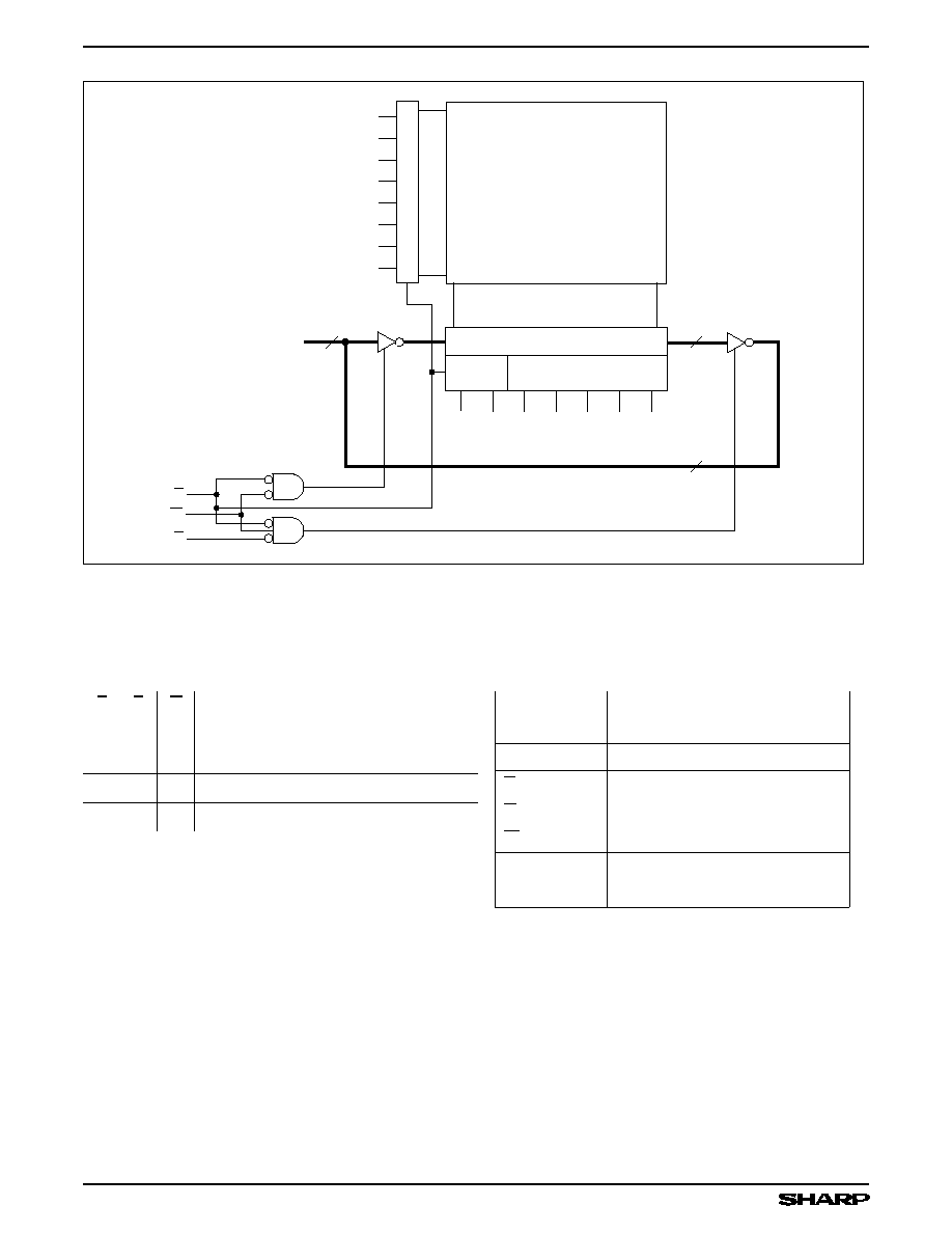
FUNCTIONAL DESCRIPTION
The LH52258A is a high-speed 262,144 bit static RAM
organized as 32K
◊
8. A fast, efficient design is obtained
with a CMOS periphery and a matrix constructed with
polysilicon load memory cells.
This RAM is fully static in operation. The Chip Enable
(E) control permits Read and Write operations when
active (LOW) or places the RAM in a low-power standby
mode when inactive (HIGH). Standby power (I
SB1
) drops
to its lowest level if E is raised to within 0.2 V of V
CC
.
Write cycles occur when both Chip Enable (E) and
Write Enable (W) are LOW. Data is transferred from the
DQ pins to the memory location specified by the 15
address lines. The proper use of the Output Enable
control (G) can prevent bus contention.
When E is LOW and W is HIGH, a static Read will
occur at the memory location specified by the address
lines. G must be brought LOW to enable the outputs.
Since the device is fully static in operation, new Read
cycles can be performed by simply changing the address.
High-frequency design techniques should be em-
ployed to obtain the best performance from this device.
Solid, low-impedance power and ground planes, with
high-frequency decoupling capacitors, are recom-
mended. Series termination of the inputs should be con-
sidered when transmission line effects occur.
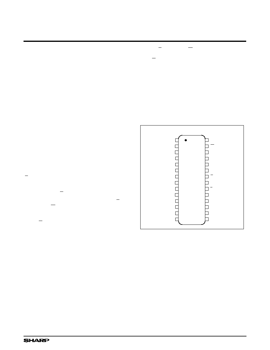
PIN CONNECTIONS
52258A-1D
1
2
3
4
5
6
7
8
9
10
11
12
A
14
A
12
A
7
A
6
A
5
A
4
A
3
A
2
A
1
A
0
V
SS
28
27
26
25
24
23
22
21
20
19
V
CC
W
A
8
A
9
A
11
G
A
10
DQ
7
DQ
6
DQ
5
18
17
DQ
3
13
14
16
15
DQ
0
DQ
4
A
13
DQ
1
DQ
2
E
28-PIN DIP
28-PIN SOJ
TOP VIEW
Figure 1. Pin Connections for DIP and
SOJ Packages
1
TRUTH TABLE
E
G
W
MODE
DQ
I
CC
H
X
X
Not Selected
High-Z
Standby
L
H
H
Selected
High-Z
Active
L
L
H
Read
Data Out
Active
L
X
L
Write
Data In
Active
PIN DESCRIPTIONS
PIN
DESCRIPTION
A
0
≠ A
14
Address Inputs
DQ
0
≠ DQ
7
Data Inputs/Outputs
E
Chip Enable
G
Output Enable
W
Write Enable
V
CC
Positive Power Supply
V
SS
Ground
52258A-2
MEMORY ARRAY
(32,768 x 8)
I/O CIRCUIT
BLOCK
DECODE
COLUMN
DECODE
A
0
A
3
A
10
A
11
A
9
A
8
A
13
E
W
A
4
A
5
A
1
A
2
A
6
A
7
A
12
A
14
G
DQ
0
- DQ
7
8
8
8
ROW DECODER
Figure 2. LH52258A Block Diagram
LH52258A
CMOS 32K
◊
8 Static RAM
2
ABSOLUTE MAXIMUM RATINGS
1
PARAMETER
RATING
V
CC
to V
SS
Potential
≠0.5 V to 7 V
Input Voltage Range
≠0.5 V to V
CC
+ 0.5 V
DC Output Current
2
±
40 mA
Storage Temperature Range
≠65
o
to 150
o
C
Power Dissipation (Package Limit)
1.0 W
NOTES:
1.
Stresses greater than those listed under `Absolute Maximum Ratings' may cause permanent damage to the device. This is a stress rating for
transient conditions only. Functional operation of the device at these or any other conditions above those indicated in the `Operating Range'
section of this specification is not implied. Exposure to absolute maximum rating conditions for extended periods may affect reliability.
2.
Outputs should not be shorted for more than 30 seconds. No more than one output should be shorted at any time.
OPERATING RANGES
SYMBOL
PARAMETER
MIN
TYP
MAX
UNIT
T
A
Temperature, Ambient
0
70
o
C
V
CC
Supply Voltage
4.5
5.0
5.5
V
V
SS
Supply Voltage
0
0
0
V
V
IL
Logic `0' Input Voltage
1
≠0 .5
0.8
V
V
IH
Logic `1' Input Voltage
2.2
V
CC
+ 0.5
V
NOTE:
1.
Negative undershoot of up to 3.0 V is permitted once per cycle.
DC ELECTRICAL CHARACTERISTICS
SYMBOL
PARAMETER
TEST CONDITIONS
MIN
TYP
1
MAX
UNIT
I
CC1
Operating Current
2
t
RC
= 20 ns
G
V
IH
, E
V
IL
, I
OUT
= 0 mA,
t
CYCLE
= 20 ns
95
150
mA
I
CC1
Operating Current
2
t
RC
= 25 ns
G
V
IH
, E
V
IL
, I
OUT
= 0 mA,
t
CYCLE
= 25 ns
90
140
mA
I
SB1
Standby Current
E
V
CC
≠ 0.2 V
0.005
1
mA
I
SB2
Standby Current
E
V
IH
6
15
mA
I
LI
Input Leakage Current
V
CC
= 5.5 V, V
IN
= 0 V to V
CC
≠2
2
µ
A
I
LO
I/O Leakage Current
V
CC
= 5.5 V, V
IN
= 0 V to V
CC
≠2
2
µ
A
V
OH
Output High Voltage
I
OH
= ≠4.0 mA
2.4
V
V
OL
Output Low Voltage
I
OL
= 8.0 m A
0.4
V
V
DR
Data Retention Voltage
E
V
CC
≠ 0.2 V
2
5.5
V
I
DR
Data Retention Current
V
CC
= 3 V, E
V
CC
≠ 0.2 V
250
µ
A
NOTES:
1.
Typical values at V
CC
= 5 V, T
A
= 25
∞
C.
2.
I
CC
is dependent upon output loading and cycle rates. Specified values are with outputs open, operating at specified cycle times.
CMOS 32K
◊
8 Static RAM
LH52258A
3
AC TEST CONDITIONS
PARAMETER
RATING
Input Pulse Levels
V
SS
to 3 V
Input Rise and Fall Times
3 ns
Input and Output Timing Ref. Levels
1.5 V
Output Load, Timing Tests
Figure 3
CAPACITANCE
1,2
PARAMETER
RATING
C
IN
(Input Capacitance)
7 pF
C
DQ
(I/O Capacitance)
8 pF
NOTES:
1.
Capacitances are maximum values at 25
o
C measured at 1.0 MHz
with V
Bias
= 0 V and V
CC
= 5.0 V.
2.
Guaranteed but not tested.
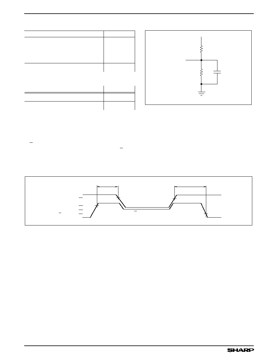
DATA RETENTION TIMING
E must be held above the lesser of V
IH
or V
CC
≠ 0.2 V
to prevent improper operation when V
CC
< 4.5 V. E must
be V
CC
≠ 0.2 V or greater to meet I
DR
specification. All
other inputs are `Don't Care.'
480
DQ PINS
52258A-3
* INCLUDES JIG AND SCOPE CAPACITANCES
255
30 pF *
+5 V
Figure 3. Output Load Circuit
t
RC
MIN
0 ns
4.5 V
V
IH
V
IL
V
CC
52258A-4
E
V
DR
E
V
DR
- 0.2 V
Figure 4. Data Retention Timing
LH52258A
CMOS 32K
◊
8 Static RAM
4
AC ELECTRICAL CHARACTERISTICS
1
(Over Operating Range)
SYMBOL
DESCRIPTION
≠2 0
≠25
UNITS
MIN
MAX
MIN
MAX
READ CYCLE
t
RC
Read Cycle Time
20
25
ns
t
AA
Address Access Time
20
25
ns
t
OH
Output Hold from Address Change
4
4
ns
t
EA
E Low to Valid Data
20
25
ns
t
ELZ
E Low to Output Active
2,3
4
4
ns
t
EHZ
E High to Output High-Z
2,3
0
10
0
12
ns
t
GA
G Low to Valid Data
10
12
ns
t
GLZ
G Low to Output Active
2,3
0
0
ns
t
GHZ
G High to Output High-Z
2,3
0
9
0
10
ns
t
PU
E Low to Power Up Time
3
0
0
ns
t
PD
E High to Power Down Time
3
25
30
ns
WRITE CYCLE
t
WC
Write Cycle Time
20
25
ns
t
EW
E Low to End of Write
15
20
ns
t
AW
Address Valid to End of Write
15
20
ns
t
AS
Address Setup
0
0
ns
t
AH
Address Hold from End of Write
0
0
ns
t
WP
W Pulse Width
12
15
ns
t
DW
Input Data Setup Time
10
12
ns
t
DH
Input Data Hold Time
0
0
ns
t
WHZ
W Low to Output High-Z
2,3
8
10
ns
t
WLZ
W High to Output Active
2,3
0
0
ns
NOTES:
1.
AC Electrical Characteristics specified at `AC Test Conditions' levels.
2.
Active output to High-Z and High-Z to output active tests specified for a
±
500 mV transition from steady state levels into the test load. The test
load has 5 pF capacitances.
3.
Guaranteed by design but not tested.
CMOS 32K
◊
8 Static RAM
LH52258A
5
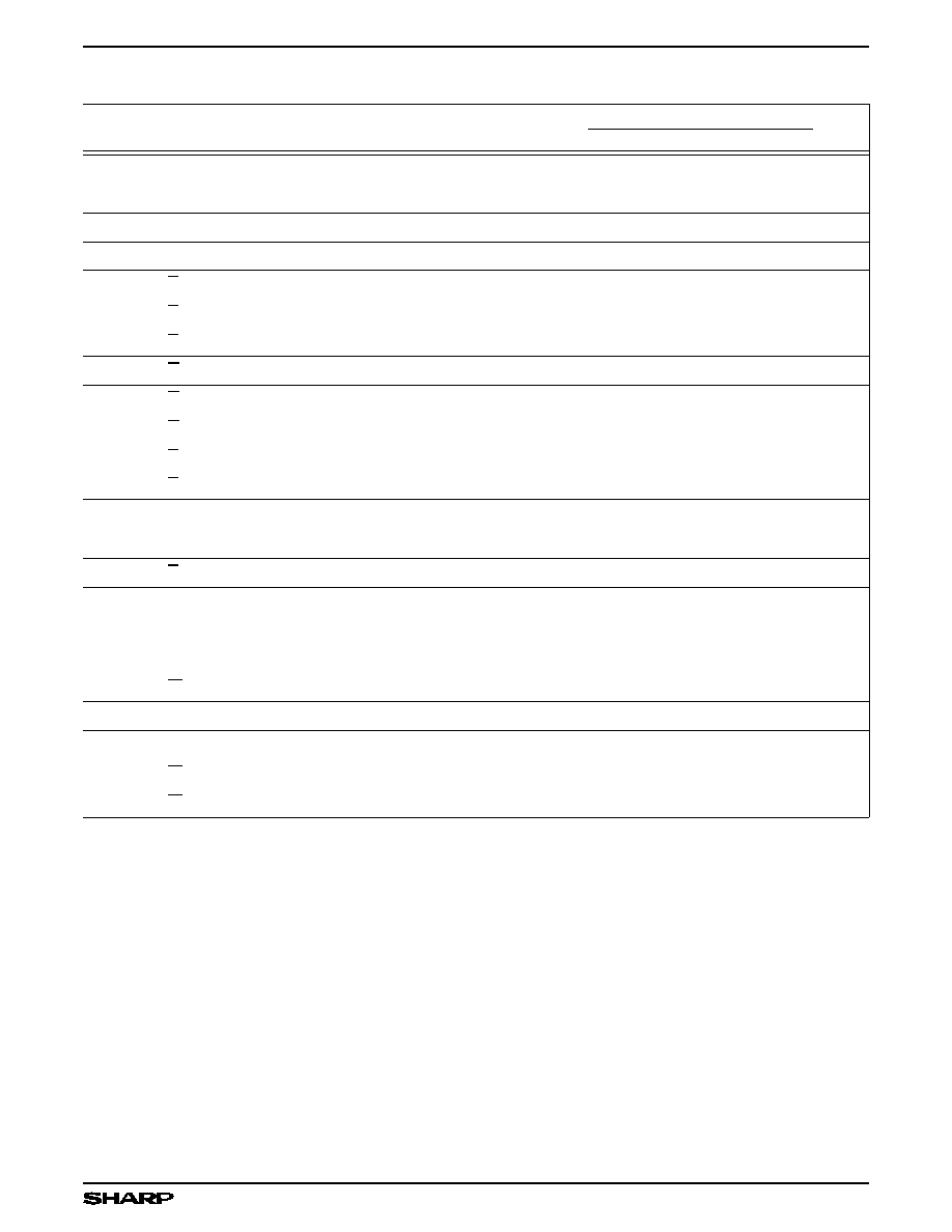
TIMING DIAGRAMS ≠ READ CYCLE
Read Cycle No. 1
Chip is in Read Mode: W is HIGH, E is LOW and G is
LOW. Read cycle timing is referenced from when all
addresses are stable until the first address transition.
Crosshatched portion of Data Out implies that data lines
are in the Low-Z state but the data is not guaranteed to
be valid until t
AA
.
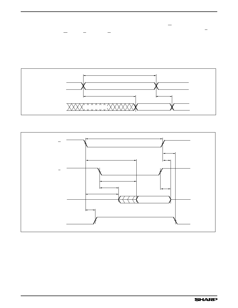
Read Cycle No. 2
Chip is in Read Mode: W is HIGH. Timing illustrated
for the case when addresses are valid before E goes
LOW. Data Out is not specified to be valid until t
EA
or t
GA
,
but may become valid as soon as t
ELZ
or t
GLZ
. Outputs
will transition from High-Z to Valid Data Out. Valid data will
be present following t
GA
only if t
EA
timing is met.
t
RC
VALID ADDRESS
t
AA
t
OH
VALID DATA
ADDRESS
DQ
52258A-5
PREVIOUS DATA
Figure 5. Read Cycle No. 1
VALID DATA
E
DQ
t
RC
t
ELZ
t
GHZ
52258A-6
G
t
EHZ
t
EA
t
PU
SUPPLY
CURRENT
t
PD
t
GLZ
t
GA
Figure 6. Read Cycle No. 2
LH52258A
CMOS 32K
◊
8 Static RAM
6
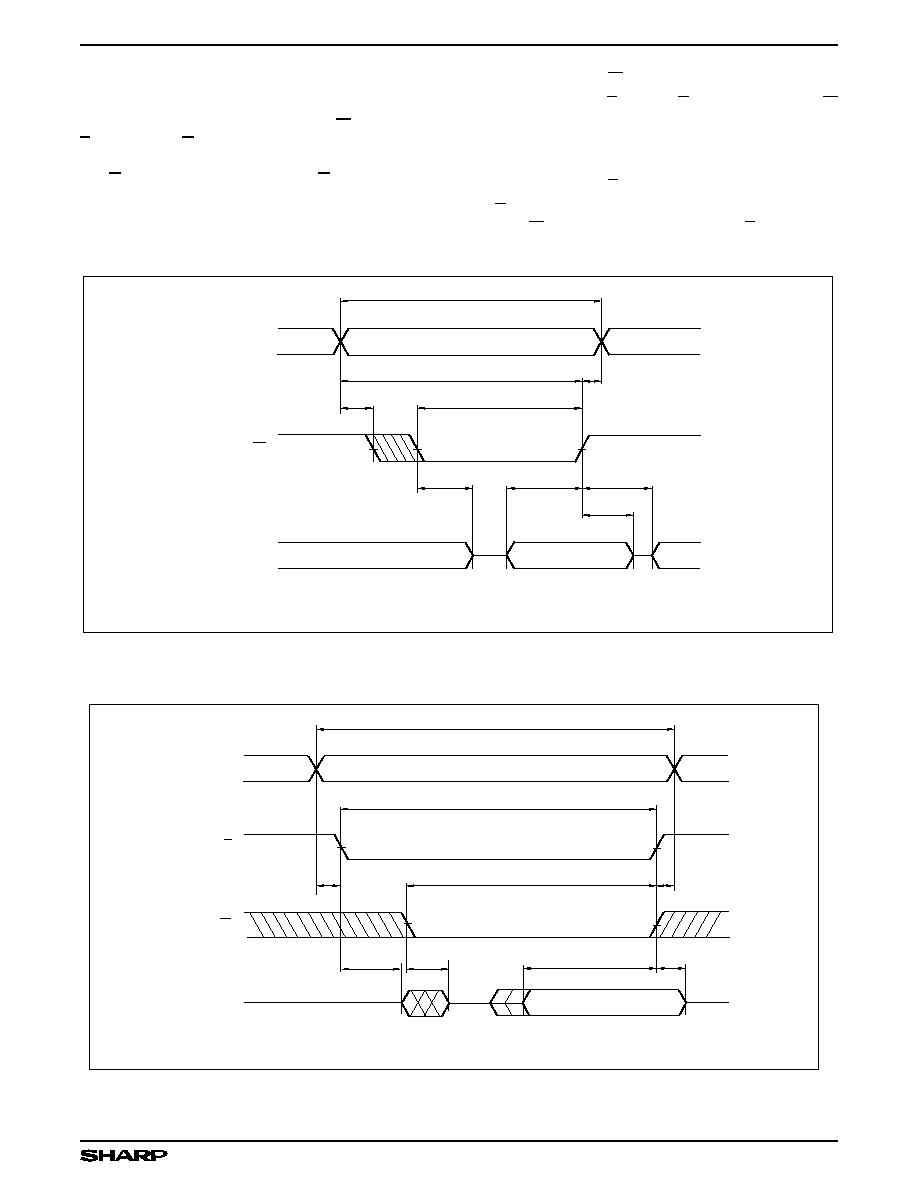
TIMING DIAGRAMS ≠ WRITE CYCLE
Addresses must be stable during Write cycles. The
outputs will remain in the High-Z state if W is LOW when
E goes LOW. If G is HIGH, the outputs will remain in the
High-Z state. Although these examples illustrate timing
with G active, it is recommended that G be held HIGH for
all Write cycles. This will prevent the LH52258A's outputs
from becoming active, preventing bus contention, thereby
reducing system noise.
Write Cycle No. 1 (W Controlled)
Chip is selected: E is LOW, G is LOW. Using only W
to control Write cycles may not offer the best performance
since both t
WHZ
and t
DW
timing specifications must be
met.
Write Cycle No. 2 (E Controlled)
G is LOW. DQ lines may transition to Low-Z if the falling
edge of W occurs after the falling edge of E.
t
WC
VALID ADDRESS
ADDRESS
52258A-7
t
AW
t
AH
t
WP
t
AS
t
WHZ
t
WLZ
t
DH
HIGH-Z
W
DQ
DATA ON
DQ LINES
PREVIOUS OUTPUT
INPUT
t
DW
LOW-Z
Figure 7. Write Cycle No. 1
t
WC
VALID ADDRESS
ADDRESS
52258A-8
W
E
DQ
t
WP
t
EW
t
AH
t
DW
t
DH
t
ELZ
t
AS
DATA ON
DQ LINES
HIGH-Z
LOW-Z
HIGH-Z
INPUT
t
WHZ
Figure 8. Write Cycle No. 2
CMOS 32K
◊
8 Static RAM
LH52258A
7
28SK-DIP (DIP028-P-0300)
DIMENSIONS IN MM [INCHES]
MAXIMUM LIMIT
MINIMUM LIMIT
1
14
15
28
28DIP-1
7.05 [0.278]
6.65 [0.262]
0.51 [0.020] MIN.
4.40 [0.173]
4.00 [0.157]
3.40 [0.134]
3.00 [0.118]
2.54 [0.100]
TYP.
0.56 [0.022]
0.36 [0.014]
0.35 [0.014]
0.15 [0.006]
DETAIL
35.00 [1.378]
34.40 [1.354]
0
∞
TO 15
∞
3.65 [0.144]
3.25 [0.128]
7.62 [0.300]
TYP.
28-pin, 300-mil DIP
PACKAGE DIAGRAMS
28SOJ300
DIMENSIONS IN MM [INCHES]
MAXIMUM LIMIT
MINIMUM LIMIT
28SOJ (SOJ28-P-300)
1.27 [0.050]
TYP.
0.53 [0.021]
0.33 [0.013]
DETAIL
7.9 [0.311]
7.5 [0.295]
8.63 [0.340]
8.23 [0.324]
18.7 [0.736]
18.3 [0.720]
1.15 [0.045]
0.85 [0.033]
0.64 [0.025] MIN
7.0 [0.276]
6.6 [0.260]
2.6 [0.102]
2.2 [0.087]
3.7 [0.146]
3.3 [0.130]
0.20 [0.008]
0.8 [0.031]
0.6 [0.024]
0.102 [0.004]
1
14
28
15
28-pin, 300-mil SOJ
LH52258A
CMOS 32K
◊
8 Static RAM
8
20
25
Access Time (ns)
D 28-pin, 300-mil DIP (DIP28-P-300)
K 28-pin, 300-mil SOJ (SOJ28-P-300)
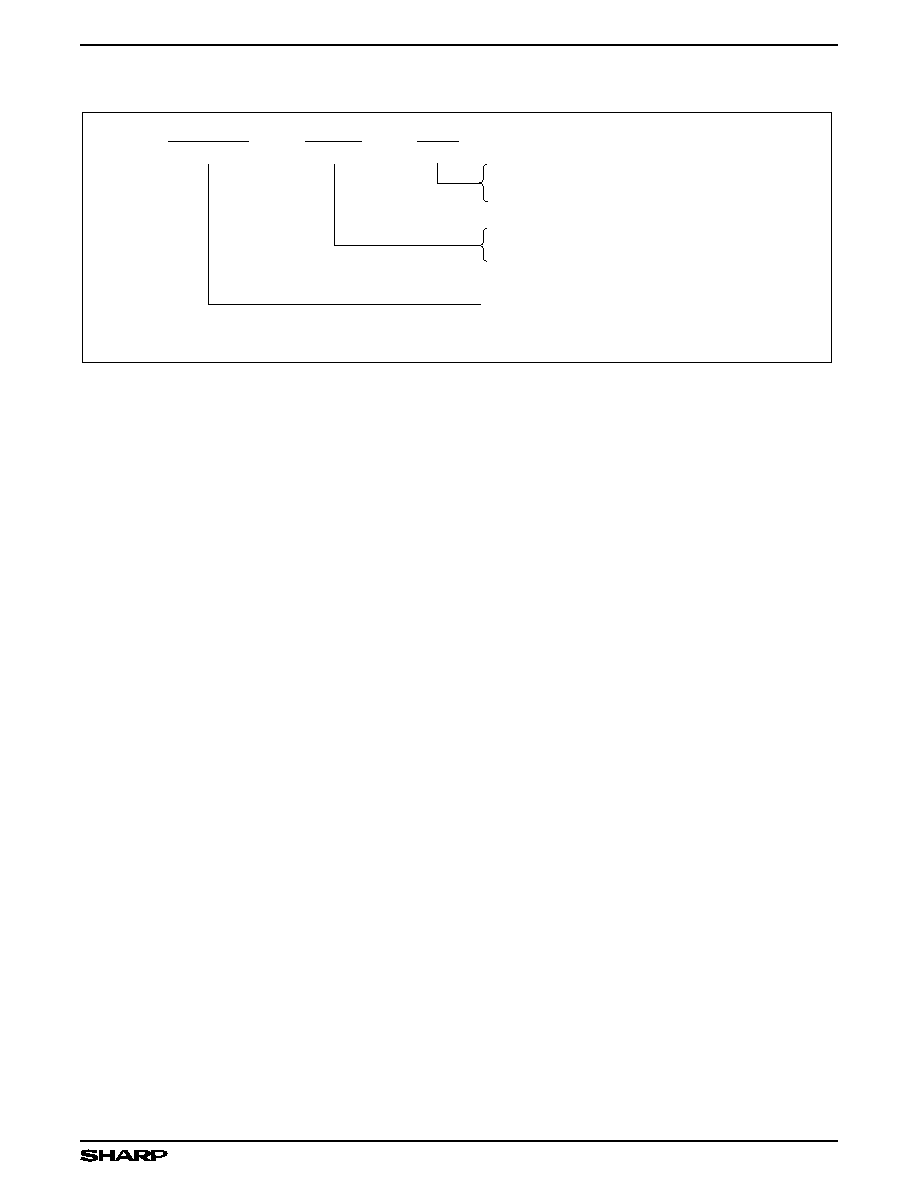
LH52258A
Device Type
X
Package
- ##
Speed
52258AMD
CMOS 32K x 8 Static RAM
Example: LH52258AK-25 (CMOS 32K x 8 Static RAM, 25 ns, 28-pin, 300-mil SOJ)
ORDERING INFORMATION
CMOS 32K
◊
8 Static RAM
LH52258A
9