 | –≠–ª–µ–∫—Ç—Ä–æ–Ω–Ω—ã–π –∫–æ–º–ø–æ–Ω–µ–Ω—Ç: LH540205 | –°–∫–∞—á–∞—Ç—å:  PDF PDF  ZIP ZIP |
LH540205
CMOS 8192
◊
9 Asynchronous FIFO
FEATURES
∑∑
Fast Access Times: 20/25/35/50 ns
∑∑
Fast-Fall-Through Time Architecture Based on
CMOS Dual-Port SRAM Technology
∑∑
Input Port and Output Port Have Entirely
Independent Timing
∑∑
Expandable in Width and Depth
∑∑
Full, Half-Full, and Empty Status Flags
∑∑
Data Retransmission Capability
∑∑
TTL-Compatible I/O
∑∑
Pin and Functionally Compatible with Am/IDT7205
∑∑
Control Signals Assertive-LOW for Noise Immunity
∑∑
Package: 28-Pin, 300-mil PDIP
FUNCTIONAL DESCRIPTION
The LH540205 is a FIFO (First-In, First-Out) memory
device, based on fully-static CMOS dual-port SRAM tech-
nology, capable of storing up to 8192 nine-bit words. It
follows the industry-standard architecture and package
pinouts for nine-bit asynchronous FIFOs. Each nine-bit
LH540205 word may consist of a standard eight-bit byte,
together with a parity bit or a block-marking/framing bit.
The input and output ports operate entirely inde-
pendently of each other, unless the LH540205 becomes
either totally full or else totally empty. Data flow at a port
is initiated by asserting either of two asynchronous, as-
sertive-LOW control inputs: Write (W) for data entry at the
input port, or Read (R) for data retrieval at the output port.
Full, Half-Full, and Empty status flags monitor the
extent to which the internal memory has been filled. The
system may make use of these status outputs to avoid
the risk of data loss, which otherwise might occur either
by attempting to write additional words into an already-full
LH540205, or by attempting to read additional words from
an already-empty LH540205. When an LH540205 is
operating in a depth-cascaded configuration, the Half-Full
Flag is not available.
Data words are read out from the LH540205's output
port in precisely the same order that they were written in
at its input port; that is, according to a First-In, First Out
(FIFO) queue discipline. Since the addressing sequence
for a FIFO device's memory is internally predefined, no
external addressing information is required for the opera-
tion of the LH540205 device.
Drop-in-replacement compatibility is maintained with
both larger sizes and smaller sizes of industry-standard
nine-bit asynchronous FIFOs. The only change is in the
number of internally-stored data words implied by the
states of the Full Flag and the Half-Full Flag.
The Retransmit (RT) control signal causes the internal
FIFO-memory-array read-address pointer to be set back
to zero, to point to the LH540205's first physical memory
location, without affecting the internal FIFO-memory-
array write-address pointer. Thus, the Retransmit control
signal provides a mechanism whereby a block of data,
delimited by the zero physical address and the current
write-address-pointer value, may be read out
repeatedly
an arbitrary number of times. The only restrictions are that
neither the read-address pointer nor the write-address
pointer may `wrap around' during this entire process, i.e.,
advance past physical location zero after traversing the
entire memory. The retransmit facility is not available
when an LH540205 is operating in a depth-expanded
configuration.
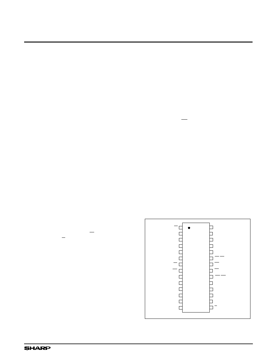
PIN CONNECTIONS
540205-2D
1
2
3
4
5
6
7
8
9
10
11
12
13
14
W
D
8
D
3
D
2
D
1
D
0
XI
FF
Q
0
Q
1
Q
2
Q
3
Q
8
V
SS
28
27
26
25
24
23
22
21
20
19
18
17
16
15
D
7
FL/RT
RS
EF
XO/HF
Q
5
Q
4
R
Q
6
Q
7
D
6
D
5
D
4
V
CC
28-PIN PDIP
TOP VIEW
Figure 1. Pin Connections for PDIP Packages
1
The Reset (RS) control signal returns the LH540205
to an initial state, empty and ready to be filled. An
LH540205 should be reset during every system power-up
sequence. A reset operation causes the internal FIFO-
memory-array write-address pointer, as well as the read-
address pointer, to be set back to zero, to point to the
LH540205's first physical memory location. Any informa-
tion which previously had been stored within the
LH540205 is not recoverable after a reset operation.
A cascading (depth-expansion) scheme may be imple-
mented by using the Expansion In (XI) input signal and
the Expansion Out (XO/HF) output signal. This scheme
allows a deeper `effective FIFO' to be implemented by
using two or more individual LH540205 devices, without
incurring additional latency (`fallthrough' or `bub-
blethrough') delays, and without the necessity of storing
and retrieving any given data word more than once. In this
cascaded operating mode, one LH540205 device must
be designated as the `first-load' or `master' device, by
grounding its First-Load (FL/RT) control input; the remain-
ing LH540205 devices are designated as `slaves,' by tying
their FL/RT inputs HIGH. Because of the need to share
control signals on pins, the Half-Full Flag and the retrans-
mission capability are not available for either `master' or
`slave' LH540205 devices operating in cascaded mode.
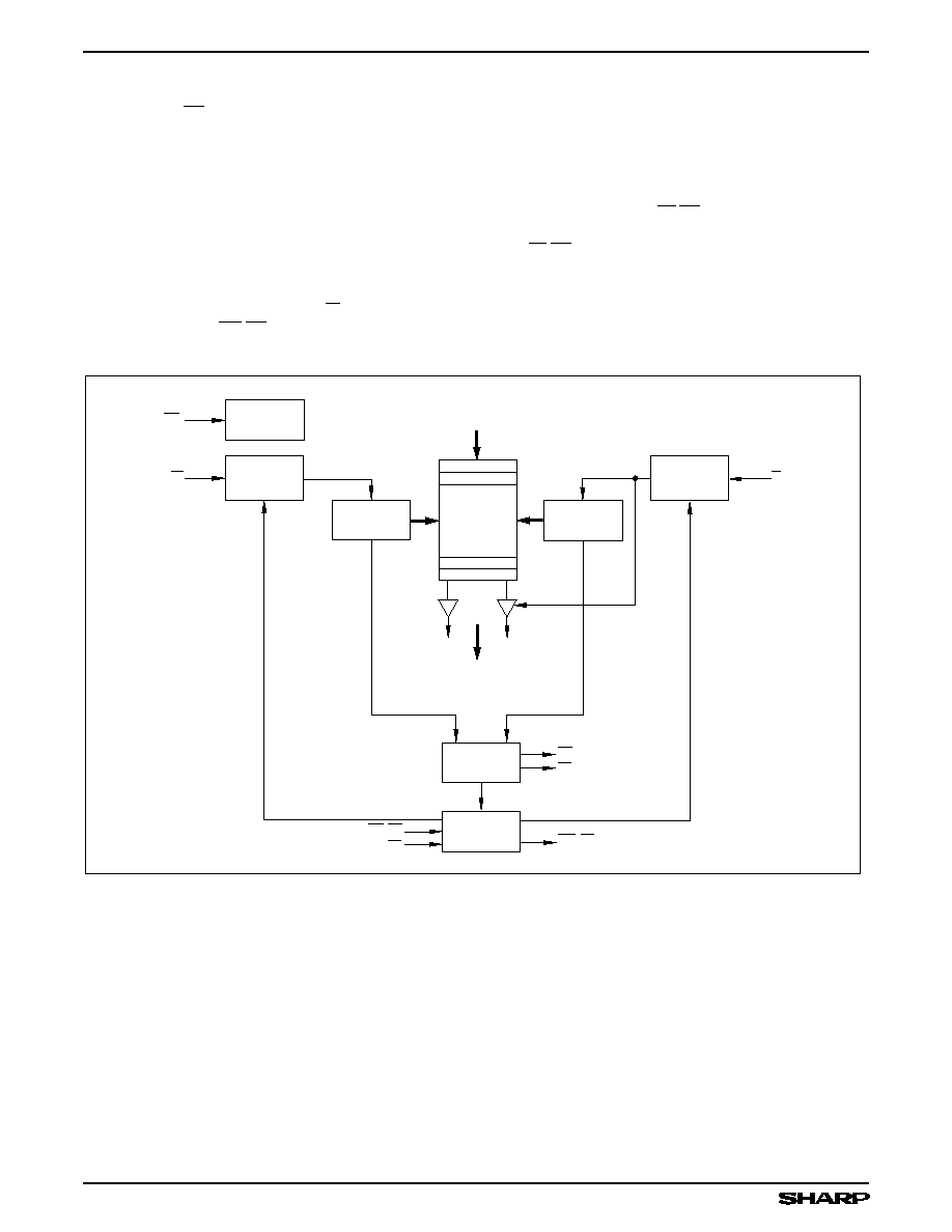
FUNCTIONAL DESCRIPTION (cont'd)
DATA OUTPUTS
Q
0
- Q
8
FLAG
LOGIC
EXPANSION
LOGIC
WRITE
POINTER
INPUT
PORT
CONTROL
READ
POINTER
DATA INPUTS
D
0
- D
8
DUAL-PORT
RAM
ARRAY
8192 x 9
R
W
XO/HF
XI
FL/RT
EF
FF
. . .
540205-1
RESET
LOGIC
RS
OUTPUT
PORT
CONTROL
Figure 2. LH540205 Block Diagram
LH540205
CMOS 8192
◊
9 Asynchronous FIFO
2

OPERATIONAL DESCRIPTION
Reset
The LH540205 is reset whenever the Reset input (RS)
is taken LOW. A reset operation initializes both the read-
address pointer and the write-address pointer to point to
location zero, the first physical memory location. During
a reset operation, the state of the XI and FL/RT inputs
determines whether the device is in standalone mode or
in depth-cascaded mode. (See Tables 1 and 2.) The
reset operation forces the Empty Flag EF to be asserted
(EF = LOW), and the Half-Full Flag HF and the Full Flag
FF to be deasserted (HF = FF = HIGH); the Data Out pins
(D
0
≠ D
8
) are forced into a high-impedance state.
A reset operation is required whenever the LH540205
first is powered up. The Read (R) and Write (W) inputs
may be in any state when the reset operation is initiated;
but they must be HIGH, before the reset operation is
terminated by a rising edge of RS, by a time t
RRSS
(for
Read) or t
WRSS
(for Write) respectively. (See Figure 9.)
Write
A write cycle is initiated by a falling edge of the Write
(W) control input. Data setup times and hold times must
be observed for the data inputs (D
0
≠ D
8
). Write opera-
tions may occur independently of any ongoing read op-
erations. However, a write operation is possible only if the
FIFO is not full, (i.e., if the Full Flag FF is HIGH).
At the falling edge of W for the first write operation after
the memory is half filled, the Half-Full Flag is asserted
(HF = LOW). It remains asserted until the difference
between the write pointer and the read pointer indicates
that the data words remaining in the LH540205 are filling
the FIFO memory to less than or equal to one-half of its
total capacity. The Half-Full Flag is deasserted
(HF = HIGH) by the appropriate rising edge of R. (See
Table 3.)
The Full Flag is asserted (FF = LOW) at the falling edge
of W for the write operation which fills the last available
location in the FIFO memory array. FF = LOW inhibits
further write operations until FF is cleared by a valid read
operation. The Full Flag is deasserted (FF = HIGH) after
the next rising edge of R releases another memory loca-
tion. (See Table 3.)
Read
A read cycle is initiated by a falling edge of the Read
(R) control input. Read data becomes valid at the data
outputs (Q
0
≠ Q
8
) after a time t
A
from the falling edge of
R. After R goes HIGH, the data outputs return to a
high-impedance state. Read operations may occur inde-
pendently of any ongoing write operations. However, a
read operation is possible only if the FIFO is not empty
(i.e., if the Empty Flag EF is HIGH).
The LH540205's internal read-address and write-
address pointers operate in such a way that consecutive
read operations always access data words in the same
order that they were written. The Empty Flag is asserted
(EF = LOW) after that falling edge of R which accesses
the last available data word in the FIFO memory. EF is
deasserted (EF = HIGH) after the next rising edge of W
loads another valid data word. (See Table 3.)
Data Flow-Through
Read-data flow-through mode occurs when the Read
(R) control input is brought LOW while the FIFO is empty,
and is held LOW in anticipation of a write cycle. At the end
of the next write cycle, the Empty Flag EF momentarily is
deasserted, and the data word just written becomes
available at the data outputs (Q
0
≠ Q
8
) after a maxi-
mum time of t
WEF
+ t
A
. Additional write operations may occur
while the R input remains LOW; but only data from the
first write operation flows through to the data outputs.
Additional data words, if any, may be accessed only by
toggling R.
Write-data flow-through mode occurs when the Write
(W) input is brought LOW while the FIFO is full, and is
held LOW in anticipation of a read cycle. At the end of the
read cycle, the Full Flag momentarily is deasserted, but
then immediately is reasserted in response to W being
held LOW. A data word is written into the FIFO on the
rising edge of W, which may occur no sooner than
t
RFF
+ t
WPW
after the read operation.
PIN DESCRIPTIONS
PIN
PIN TYPE
1
DESCRIPTION
D
0
≠ D
8
I
Input Data Bus
Q
0
≠ Q
8
O/Z
Output Data Bus
W
I
Write Request
R
I
Read Request
EF
O
Empty Flag
FF
O
Full Flag
PIN
PIN TYPE
1
DESCRIPTION
XO/HF
O
Expansion Out/Half-Full Flag
XI
I
Expansion In
FL/RT
I
First Load/Retransmit
RS
I
Reset
V
CC
V
Positive Power Supply
V
SS
V
Ground
NOTE:
1.
I = Input, O = Output, Z = High-Impedance, V = Power Voltage Level
CMOS 8192
◊
9 Asynchronous FIFO
LH540205
3
OPERATIONAL DESCRIPTION (cont'd)
Retransmit
The FIFO can be made to reread previously-read data
by means of the Retransmit function. A retransmit opera-
tion is initiated by pulsing the RT input LOW. Both R and
W must be deasserted (HIGH) for the duration of the
retransmit pulse. The FIFO's internal read-address
pointer is reset to point to location zero, the first physical
memory location, while the internal write-address
pointer remains unchanged.
After a retransmit operation, those data words in the
region in between the read-address pointer and the
write-address pointer may be reaccessed by subsequent
read operations. A retransmit operation may affect the
state of the status flags FF, HF, and EF, depending on
the relocation of the read-address pointer. There is no
restriction on the number of times that a block of data
within an LH540205 may be read out, by repeating the
retransmit operation and the subsequent read operations.
The maximum length of a data block which may be
retransmitted is 8192 words. Note that if the write-address
pointer ever `wraps around' (i.e., passes location zero
more than once) during a sequence of retransmit opera-
tions, some data words will be lost.
The Retransmit function is not available when the
LH540205 is operating in depth-cascaded mode,
because the FL/RT control pin must be used for first-load
selection rather than for retransmission control.
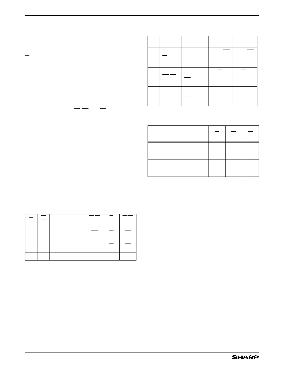
Table 1. Grouping-Mode Determination
During a Reset Operation
XI
FL/
RT
MODE
XO/HF
USAGE
XI
USAGE
FL/RT
USAGE
H
1
H
Cascaded
Slave
2
XO
XI
FL
H
1
L
Cascaded
Master
2
XO
XI
FL
L
X
Standalone
HF
(none)
RT
NOTES:
1. A reset operation forces XO HIGH for the n
th
FIFO, thus forcing
XI HIGH for the (n+1)
st
FIFO.
2. The terms `master' and `slave' refer to operation in depth-cas-
caded grouping mode.
3. H = HIGH; L = LOW; X = Don't Care.
Table 2. Expansion-Pin Usage According to
Grouping Mode
I/O
PIN
STANDALONE
CASCADED
MASTER
CASCADED
SLAVE
I
XI
Grounded
From XO
(n-1st
FIFO)
From XO
(n-1st
FIFO)
O
XO/HF
Becomes
HF
To XI
(n+1st
FIFO)
To XI
(n+1st
FIFO)
I
FL/RT
Becomes
RT
Grounded
(Logic
LOW)
Logic
HIGH
Table 3. Status Flags
NUMBER OF UNREAD DATA
WORDS PRESENT WITHIN
8192
◊
9 FIFO
FF
HF
EF
0
H
H
L
1 to 4096
H
H
H
4097 to 8191
H
L
H
8192
L
L
H
LH540205
CMOS 8192
◊
9 Asynchronous FIFO
4
OPERATIONAL MODES
Standalone Configuration
When depth cascading is not required for a given
application, the LH540205 is placed in standalone mode
by tying the Expansion In input (XI) to ground. This
input is internally sampled during a reset operation. (See
Table 1.)
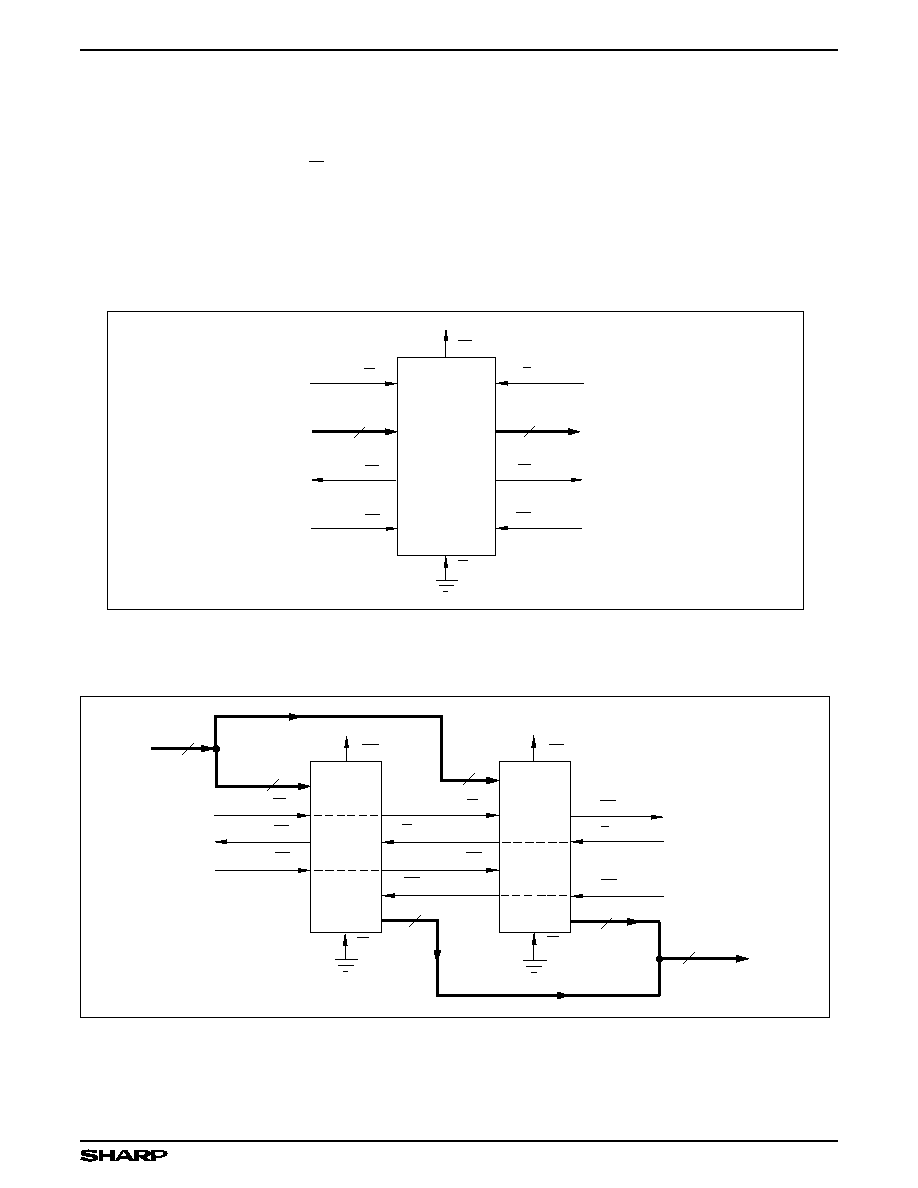
Width Expansion
Word-width expansion is implemented by placing mul-
tiple LH540205 devices in parallel. Each LH540205
should be configured for standalone mode. In this ar-
rangement, the behavior of the status flags is identical for
all devices; so, in principle, a representative value for
each of these flags could be derived from any one device.
In practice, it is better to derive `composite' flag values
using external logic, since there may be minor speed
variations between different actual devices. (See Figures
3 and 4.)
WRITE
DATA IN
D
0
- D
8
9
FULL FLAG
RESET
XI
RT
RETRANSMIT
EMPTY FLAG
9
READ
HF
LH540205
W
FF
RS
R
EF
DATA OUT
Q
0
- Q
8
540205-17
Figure 3. Standalone FIFO (8192
◊
9)
18
WRITE
FULL FLAG
RESET
9
READ
EMPTY FLAG
R
EF
XI
RT
R
W
540205-18
RS
RETRANSMIT
RT
XI
HF
W
FF
RS
9
18
9
HF
9
LH540205
LH540205
DATA IN
D
0
- D
17
DATA OUT
Q
0
- Q
17
Figure 4. FIFO Word-Width Expansion (8192
◊
18)
CMOS 8192
◊
9 Asynchronous FIFO
LH540205
5