LH5P1632
CMOS 512K (32K
◊
16) Pseudo-Static RAM
FEATURES
∑∑
32,768
◊
16 bit organization
∑∑
Access time: 80/150 ns (MAX.)
∑∑
Cycle time: 140/210 ns (MIN.)
∑∑
Single +5 V power supply
∑∑
Power consumption (MAX.):
Operating: 467.5/327.5 mW
Standby: 16.5 mW
∑∑
TTL compatible I/O
∑∑
256 refresh cycles/4 ms (MAX.)
∑∑
Available for auto-refresh mode
∑∑
Packages:
40-pin, 600-mil DIP
40-pin, 525-mil SOP
DESCRIPTION
The LH5P1632 is a 512K-bit Pseudo-Static RAM
organized as 32,768
◊
16 bits. It is fabricated using
silicon-gate CMOS process technology.
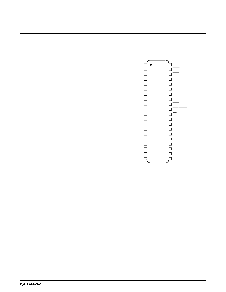
PIN CONNECTIONS
5P1632-1
TOP VIEW
5
6
7
8
11
12
I/O
1
A
2
34
33
32
31
30
29
26
A
4
A
3
9
10
A
0
A
1
28
27
A
5
A
13
A
14
LOE/RFSH
13
14
15
36
35
I/O
2
A
11
I/O
4
UOE/TEST
1
CE
A
6
I/O
13
I/O
14
A
12
40-PIN DIP
40-PIN SOP
3
4
A
7
38
37
LWR
A
8
A
10
1
2
40
39
V
CC
GND
UWR
I/O
3
I/O
15
I/O
16
24
25
16
17
I/O
6
I/O
11
I/O
12
I/O
5
22
23
18
19
I/O
8
I/O
9
I/O
10
I/O
7
21
20
V
CC
GND
A
9
Figure 1. Pin Connections for DIP and
SOP Packages
1
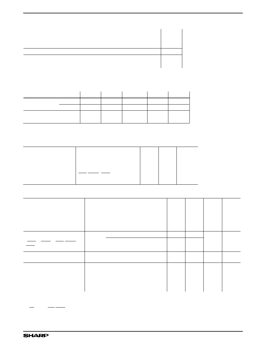
ABSOLUTE MAXIMUM RATINGS
PARAMETER
SYMBOL
RATING
UNIT
NOTE
Applied voltage on all pins
V
T
≠1.0 to +7.0
V
1
Output short circuit current
I
O
50
mA
Power dissipation
P
D
600
mW
Operating temperature
Topr
0 to +70
∞
C
Storage temperature
Tstg
≠65 to +150
∞
C
NOTE:
1.
The maximum applicable voltage on any pin with respect to GND.
RECOMMENDED OPERATING CONDITIONS (T
A
= 0 to +70
∞
C)
PARAMETER
SYMBOL
MIN.
TYP.
MAX.
UNIT
NOTE
Supply voltage
V
CC
4.5
5.0
5.5
V
GND
0
0
0
V
Input voltage
V
IH
2.4
V
CC
+ 0.3
V
V
IL
≠0.3
0.8
V
1
NOTE:
1.
V
IL
(MIN.) = ≠1.0 V when the pulse width is less than 20 ns.
CAPACITANCE (T
A
= 0 to +70
∞
C, f = 1 MHz, V
CC
= 5.0 V
±
10%)
PARAMETER
CONDITIONS
SYMBOL
MIN.
MAX.
UNIT
Input capacitance
A
0
≠ A
14
C
IN1
8
pF
LWR, UWR
C
IN2
5
pF
CE
C
IN3
5
pF
LOE/RFSH, UOE
C
IN4
5
pF
Input/Output capacitance
I/O
1
≠ I/O
16
C
OUT1
10
pF
DC CHARACTERISTICS (T
A
= 0 to +70
∞
C, V
CC
= 5.0 V
±
10%)
PARAMETER
SYMBOL
CONDITIONS
MIN.
MAX.
UNIT
NOTE
Average supply current in
normal operation
t
RC
= t
RC
(MIN)
I
CC1
LH5P1632-80
85
mA
1, 2
LH5P1632-15
65
Supply current in
standby mode
I
CC2
3.0
mA
1, 3
Average supply current in
CPU internal cycle
(LWR = UWR = LOE/RFSH =
UOE = V
IH
)
I
CC3
LH5P1632-80
85
mA
1, 2
LH5P1632-15
Input leakage current
I
LI
0 V
V
IN
6.5 V,
0 V except on test pins
≠10
10
µ
A
I/O leakage current
I
LO
0 V
V
OUT
V
CC
+ 0.3 V,
Outputs in high-impedance
state
≠10
10
µ
A
Output HIGH voltage
V
OH
I
OUT
= ≠1.0 mA
2.4
V
Output LOW voltage
V
OL
I
OUT
= 4.0 mA
0.4
V
NOTES:
1.
Specified values are with outputs open.
2.
I
CC1
and I
CC3
depend on the cycle time.
3.
CE = High, LOE/RFSH = High.
CMOS 512K (32K
◊
16) Pseudo-Static RAM
LH5P1632
3
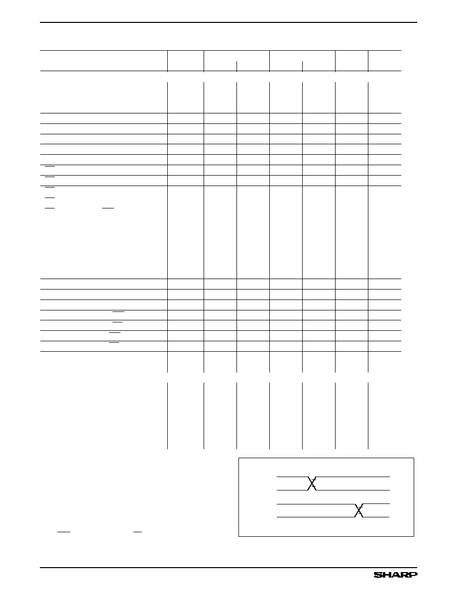
AC CHARACTERISTICS
1, 2, 3
(T
A
= 0 to +70
∞
C, V
CC
= 5.0 V
±
10%)
PARAMETER
SYMBOL
≠80 ns
≠150 ns
UNIT
NOTE
MIN.
MAX.
MIN.
MAX.
READ OR WRITE CYCLE
Random read, write cycle time
t
RC
140
210
ns
Read modify write cycle time
t
RMW
205
280
ns
CE pulse width
t
CE
80
10,000
150
10,000
ns
CE precharge time
t
P
50
60
ns
Address setup time
t
AS
0
0
ns
4
Address hold time
t
AH
20
30
ns
4
Read command setup time
t
RCS
0
0
ns
Read command hold time
t
RCH
0
0
ns
CE access time
t
CEA
80
150
ns
5
OE access time
t
OEA
30
70
ns
5
CE to output in Low-Z
t
CLZ
10
10
ns
OE to output in Low-Z
t
OLZ
0
0
ns
OE setup time for WR
t
OSW
0
0
ns
Output disable time from CE
t
CHZ
0
25
0
35
ns
Output disable time from OE
t
OHZ
0
25
0
35
ns
Output disable time from WR
t
WHZ
0
25
0
35
ns
OE setup time
t
OES
10
10
ns
OE hold time
t
OEH
0
0
ns
OE lead time
t
OEL
10
10
ns
Write command pulse width
t
WCP
60
85
ns
Write command setup time
t
WCS
60
85
ns
Write command hold time
t
WCH
60
85
ns
Data setup time from WR
t
DSW
30
50
ns
Data setup time from CE
t
DSC
30
50
ns
Data hold time from WR
t
DHW
0
0
ns
Data hold time from CE
t
DHC
0
0
ns
Transition time (rise and fall)
t
T
3
35
3
35
ns
Refresh time interval
t
REF
4
4
ms
REFRESH CYCLE
Auto refresh cycle time
t
FC
140
190
ns
Refresh delay time from CE
t
RFD
50
60
ns
Refresh pulse width (Auto Refresh)
t
FAP
30
8,000
80
8,000
ns
Refresh precharge time (Auto
Refresh)
t
FP
40
30
ns
CE delay time from Refresh active
(Auto Refresh)
t
FCE
160
225
ns
NOTES:
1.
In order to initialize the circuit, CE and OEL/RFSH should be kept
V
IH
for 200
µ
s after power on and followed by at least 8 dummy
cycles.
2.
AC characteristics shall be tested with t
T
= 5 ns.
3.
AC characteristics are measured at the following condition (see figure
at right).
4.
Address is latched at the negative edge of CE.
5.
Measured with a load equivalent to 2TTL + 100 pF.
6.
Data for the lower byte (I/O
1
to I/O
8
) is latched at the positive edge
of LWR or the positive edge of CE. Data for the upper byte (I/O
9
to
I/O
16
) is latched at the positive edge of UWR or the positive edge
of CE.
2.4 V
0.8 V
2.6 V
0.6 V
2.2 V
0.8 V
OUTPUT
INPUT
5P1632-9
Figure 3. AC Characteristics
LH5P1632
CMOS 512K (32K
◊
16) Pseudo-Static RAM
4