 | –≠–ª–µ–∫—Ç—Ä–æ–Ω–Ω—ã–π –∫–æ–º–ø–æ–Ω–µ–Ω—Ç: LH75411-3 | –°–∫–∞—á–∞—Ç—å:  PDF PDF  ZIP ZIP |

Preliminary Data Sheet
6/4/03
1
LH75400/01/10/11
Preliminary Data Sheet
System-on-Chip
DESCRIPTION
The SHARP BlueStreak LH75400/01/10/11 family
consists of four low-cost 16/32-bit System-on-Chip
(SoC) devices.
∑ LH75401 -- contains the superset of features.
∑ LH75411 -- similar to LH75401, without CAN 2.0B.
∑ LH75400 -- similar to LH75401, but with a Gray-
scale LCDC only.
∑ LH75410 -- similar to LH75400, without CAN 2.0B.
COMMON FEATURES
∑ Highly Integrated System-on-Chip
∑ ARM7TDMI-STM Core
∑ High Performance (70 MHz CPU Speed)
≠ Internal PLL Driven or External Clock Driven
≠ Crystal Oscillator/Internal PLL Can Operate with
Input Frequency Range of 14 MHz to 20 MHz
∑ 32KB On-chip SRAM
≠ 16KB Tightly Coupled Memory (TCM) SRAM
≠ 16KB Internal SRAM
∑ Clock and Power Management
≠ Low Power Modes: Standby, Sleep, Stop
∑ Eight Channel, 10-bit Analog-to-Digital Converter
∑ Integrated Touch Screen Controller
∑ Serial interfaces
≠ Two 16C550-type UARTs supporting baud rates
up to 921,600 baud (requires crystal frequency of
14.756 MHz).
≠ One 82510-type UART supporting baud rates up
to 3,225,600 baud (requires a system clock of
70 MHz).
∑ Synchronous Serial Port
≠ Motorola SPITM
≠ National Semiconductor MicrowireTM
≠ Texas Instruments SSI
∑ Real-Time Clock (RTC)
∑ Three Counter/Timers
≠ Capture/Compare/PWM Compatibility
≠ Watchdog Timer (WDT)
∑ Low-Voltage Detector
∑ JTAG Debug Interface and Boundary Scan
∑ Single 3.3 V Supply
∑ 5 V Tolerant Inputs
∑ 144-pin LQFP Package
∑ -40
∞
C to +85
∞
C Operating Temperature
Unique Features of the LH75401
∑ Color and Grayscale Liquid Crystal Display (LCD)
Controller
≠ 12-bit (4,096) Direct Mode Color, up to VGA
≠ 8-bit (256) Direct or Palletized Color, up to SVGA
≠ 4-bit (16) Direct Mode Color/Grayscale, up to XGA
≠ 12-bit Video Bus
≠ Supports STN, TFT, HR-TFT, and AD-TFT
Displays.
∑ CAN Controller that supports CAN version 2.0B.
Unique Features of the LH75411
∑ Color and Grayscale LCD Controller (LCDC)
≠ 12-bit (4,096) Direct Mode Color, up to VGA
≠ 8-bit (256) Direct or Palletized Color, up to SVGA
≠ 4-bit (16) Direct Mode Color/Grayscale, up to XGA
≠ 12-bit Video Bus
≠ Supports STN, TFT, HR-TFT, and AD-TFT
Displays.
Unique Features of the LH75400
∑ Grayscale LCDC
≠ 4-bit (16 Level) Grayscale, up to XGA
≠ 8-bit Video Bus
≠ Supports STN Displays.
∑ Controller Area Network (CAN) Controller that sup-
ports CAN version 2.0B.
Unique Features of the LH75410
∑ Grayscale LCDC
≠ 4-bit (16 Level) Grayscale, up to XGA
≠ 8-bit Video Bus
≠ Supports STN Displays.
NOTES:ARM7 Thumb, and ARM7TDMI-S are trademarks of ARM
LTD. Motorola SPI is a trademark of Motorola, Inc. Microwire
is a trademark of National Semiconductor Corporation.
VGA and XGA modes require 66 MHz CPU speed.
LH75400/01/10/11
System-on-Chip
2
6/4/03
Preliminary Data Sheet
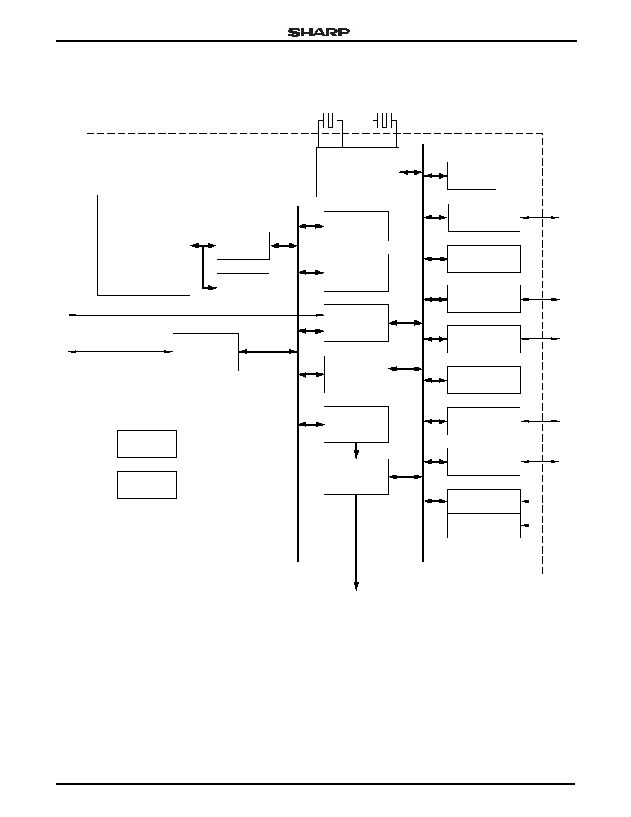
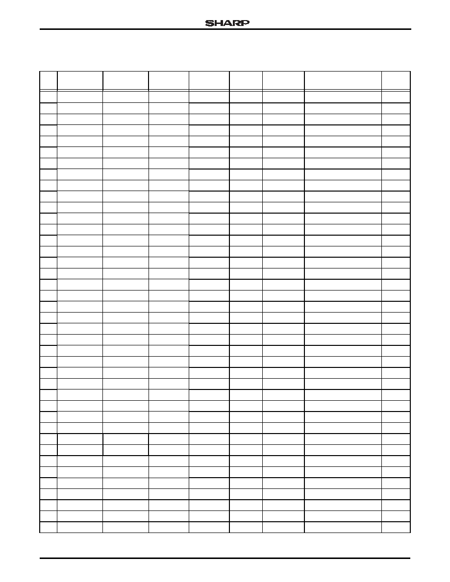
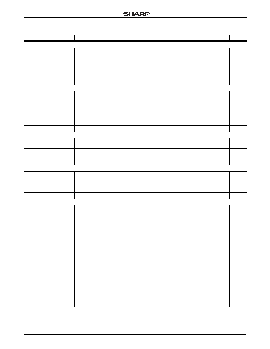
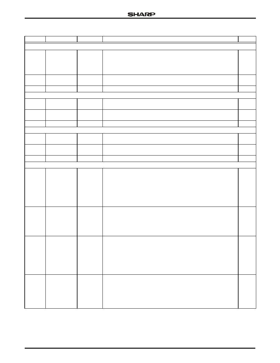
LH75401 BLOCK DIAGRAM
Figure 1. LH75401 Block Diagram
LH75401-1
OSCILLATOR,
PLL, POWER
MANAGEMENT, and
RESET CONTROL
VECTORED
INTERRUPT
CONTROLLER
INTERNAL
16KB SRAM
TCM
16KB SRAM
AHB
INTERFACE
BROWNOUT
DETECTOR
LINEAR
REGULATOR
14 to 20 MHz
32.768 kHz
REAL TIME
CLOCK
COLOR
LCD
CONTROLLER
STATIC
MEMORY
CONTROLLER
ARM7TDMI-S
ADVANCED
PERIPHERAL
BUS BRIDGE
4 CHANNEL
DMA
CONTROLLER
ADVANCED HIGH
PERFORMANCE
BUS (AHB)
ADVANCED
PERPHERAL
BUS (APB)
AD-TFT LCD
TIMING
CONTROLLER
76-BIT GENERAL
PURPOSE I/O
I/O
CONFIGURATION
SYNCHRONOUS
SERIAL PORT
TIMER (3)
WATCHDOG
TIMER
CAN 2.0B
8 CHANNEL
10-BIT ADC
TOUCH PANEL
INTERFACE
UART (3)
LH75401
System-on-Chip
LH75400/01/10/11
Preliminary Data Sheet
6/4/03
3
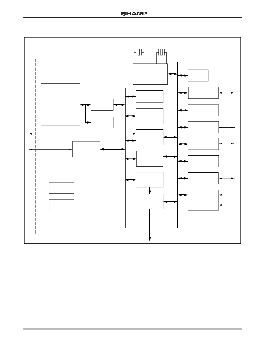
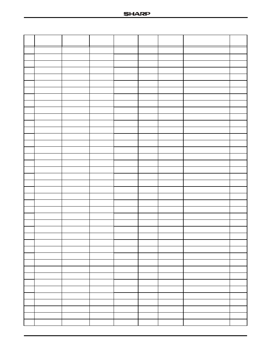
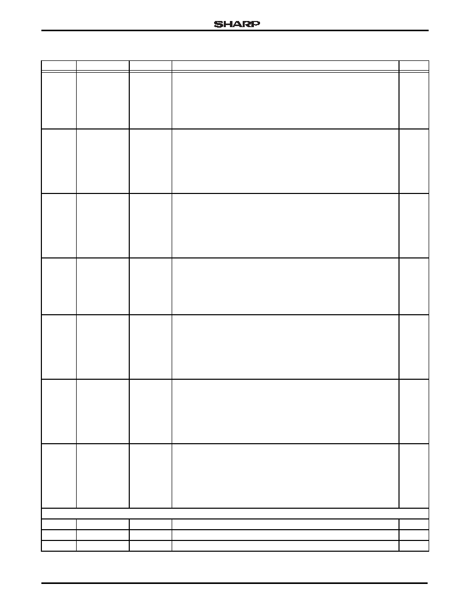
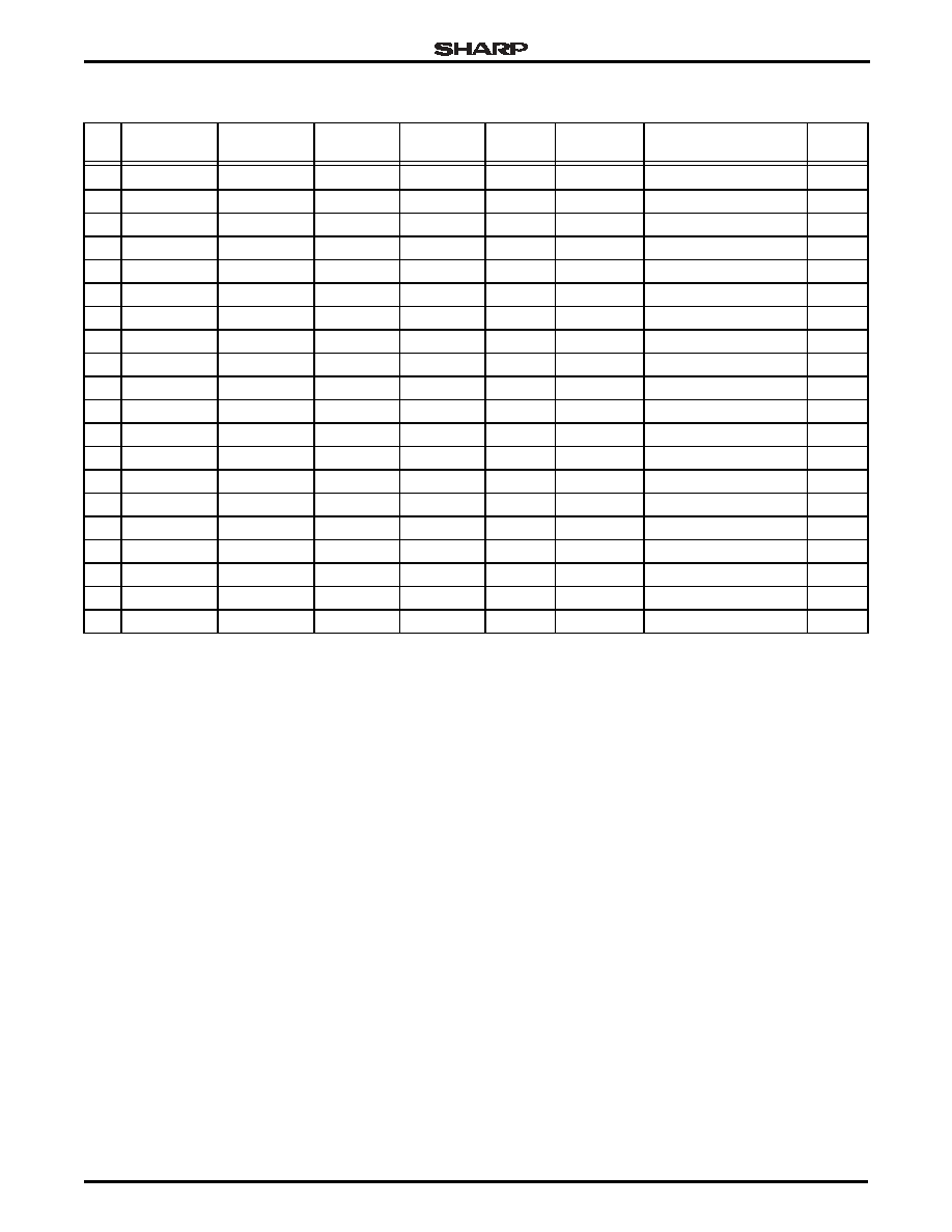
LH75411 BLOCK DIAGRAM
Figure 2. LH75411 Block Diagram
LH75411-1
OSCILLATOR,
PLL, POWER
MANAGEMENT, and
RESET CONTROL
VECTORED
INTERRUPT
CONTROLLER
INTERNAL
16KB SRAM
TCM
16KB SRAM
AHB
INTERFACE
BROWNOUT
DETECTOR
LINEAR
REGULATOR
14 to 20 MHz
32.768 kHz
REAL TIME
CLOCK
COLOR
LCD
CONTROLLER
STATIC
MEMORY
CONTROLLER
ARM 7TDMI-S
ADVANCED
PERIPHERAL
BUS BRIDGE
4 CHANNEL
DMA
CONTROLLER
ADVANCED HIGH
PERFORMANCE
BUS (AHB)
ADVANCED
PERPHERAL
BUS (APB)
AD-TFT LCD
TIMING
CONTROLLER
76-BIT GENERAL
PURPOSE I/O
I/O
CONFIGURATION
SYNCHRONOUS
SERIAL PORT
TIMER (3)
WATCHDOG
TIMER
8 CHANNEL
10-BIT ADC
TOUCH PANEL
INTERFACE
UART (3)
LH75411
LH75400/01/10/11
System-on-Chip
4
6/4/03
Preliminary Data Sheet
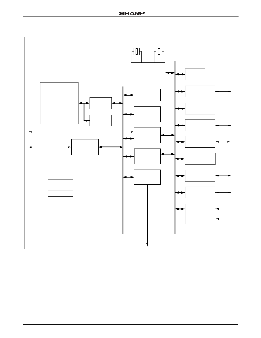
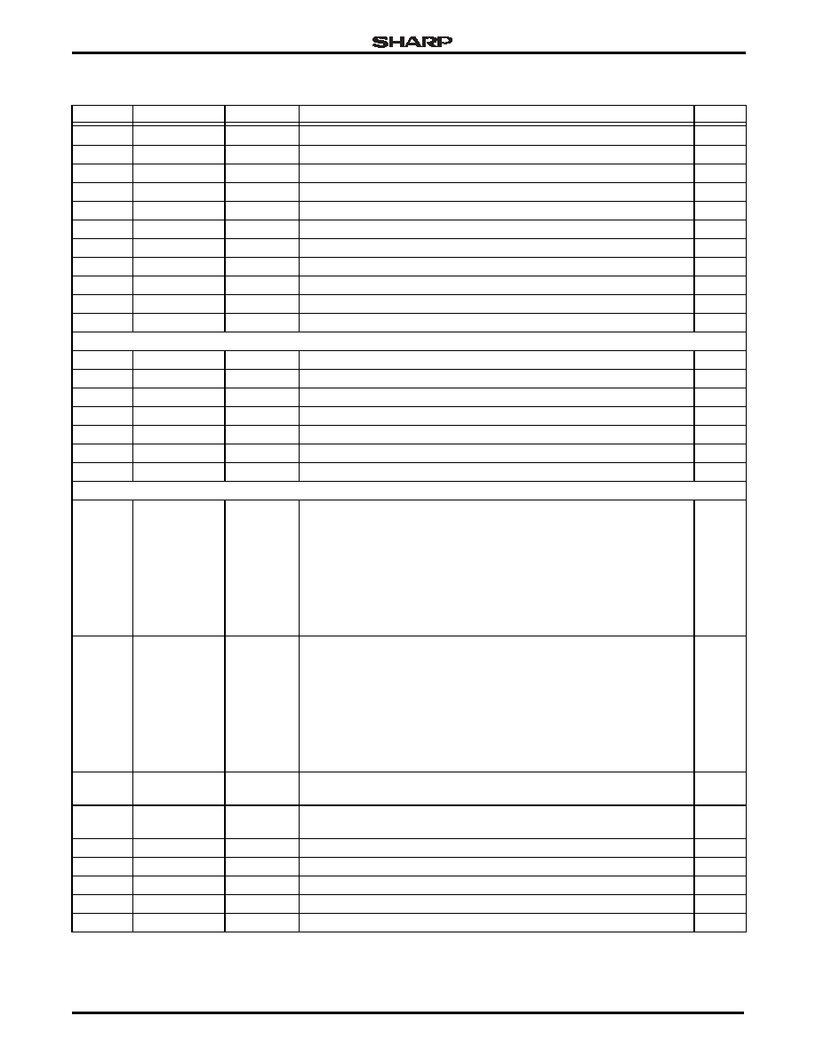
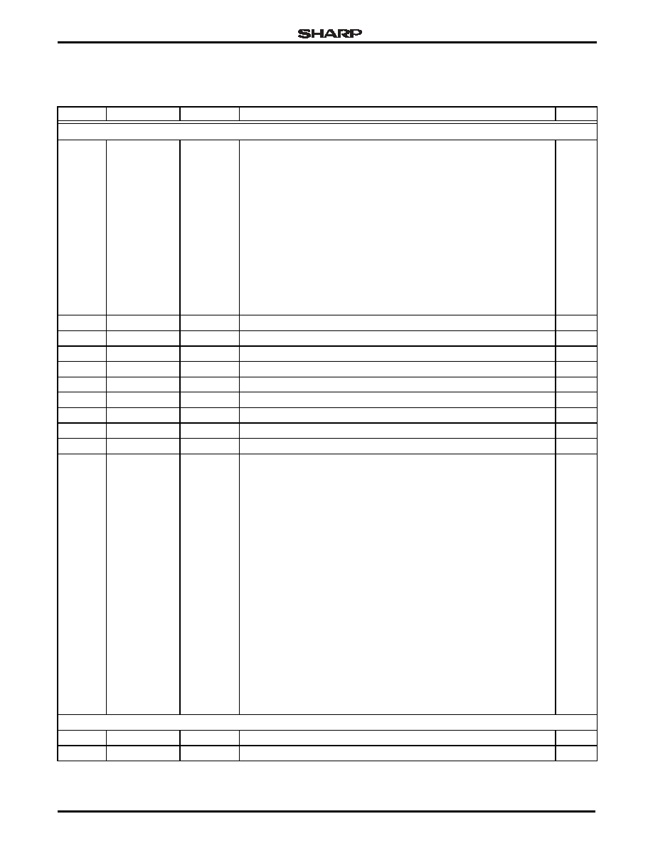
LH75400 BLOCK DIAGRAM
Figure 3. LH75400 Block Diagram
LH75400-1
OSCILLATOR,
PLL, POWER
MANAGEMENT, and
RESET CONTROL
VECTORED
INTERRUPT
CONTROLLER
INTERNAL
16KB SRAM
TCM
16KB SRAM
AHB
INTERFACE
BROWNOUT
DETECTOR
LINEAR
REGULATOR
14 to 20 MHz
32.768 kHz
REAL TIME
CLOCK
GRAYSCALE
LCD
CONTROLLER
STATIC
MEMORY
CONTROLLER
ARM 7TDMI-S
ADVANCED
PERIPHERAL
BUS BRIDGE
4 CHANNEL
DMA
CONTROLLER
ADVANCED HIGH
PERFORMANCE
BUS (AHB)
ADVANCED
PERPHERAL
BUS (APB)
76-BIT GENERAL
PURPOSE I/O
I/O
CONFIGURATION
SYNCHRONOUS
SERIAL PORT
TIMER (3)
WATCHDOG
TIMER
CAN 2.0B
8 CHANNEL
10-BIT ADC
TOUCH PANEL
INTERFACE
UART (3)
LH75400
System-on-Chip
LH75400/01/10/11
Preliminary Data Sheet
6/4/03
5
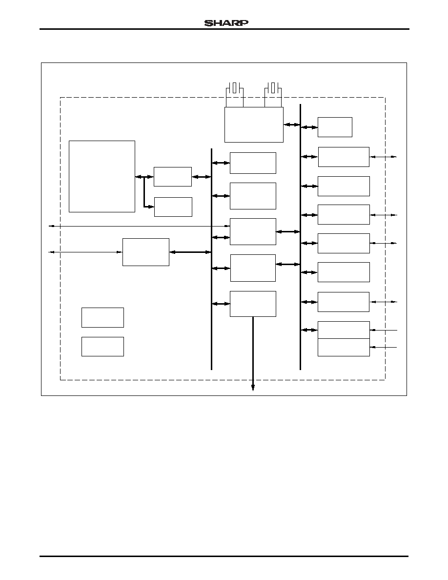
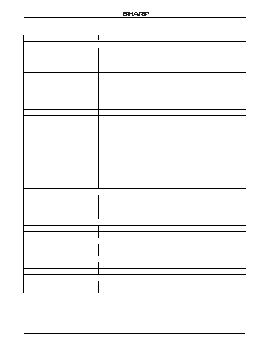
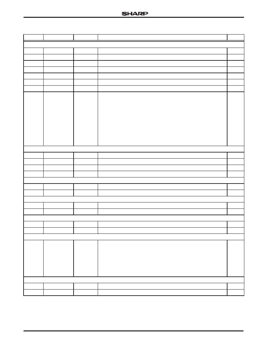
LH75410 BLOCK DIAGRAM
Figure 4. LH75410 Block Diagram
LH75410-1
OSCILLATOR,
PLL, POWER
MANAGEMENT, and
RESET CONTROL
VECTORED
INTERRUPT
CONTROLLER
INTERNAL
16KB SRAM
TCM
16KB SRAM
AHB
INTERFACE
BROWNOUT
DETECTOR
LINEAR
REGULATOR
14 to 20 MHz
32.768 kHz
REAL TIME
CLOCK
GRAYSCALE
LCD
CONTROLLER
STATIC
MEMORY
CONTROLLER
ARM 7TDMI-S
ADVANCED
PERIPHERAL
BUS BRIDGE
4 CHANNEL
DMA
CONTROLLER
ADVANCED HIGH
PERFORMANCE
BUS (AHB)
ADVANCED
PERPHERAL
BUS (APB)
76-BIT GENERAL
PURPOSE I/O
I/O
CONFIGURATION
SYNCHRONOUS
SERIAL PORT
TIMER (3)
WATCHDOG
TIMER
8 CHANNEL
10-BIT ADC
TOUCH PANEL
INTERFACE
UART (3)
LH75410

LH75400/01/10/11
System-on-Chip
6
6/4/03
Preliminary Data Sheet
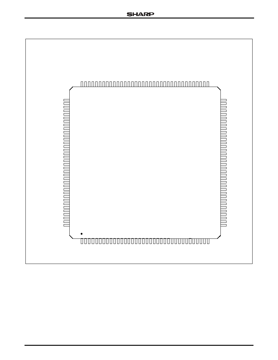
THE LH75401
Figure 5. LH75401 Pin Diagram
45
44
43
42
41
40
39
38
37
PH7/LCDDCLK
VDD
VSS
PH6/LCDLP/LCDHRLP
PH5/LCDFP/LCDSPS
PH4/LCDEN/LCDSPL
PH3/ LCDVD11
PH2/ LCDVD10
PH1/LCDVD9
VDD
PH0/LCDVD8
PI7/LCDVD7
PI6/LCDVD6
PI5/LCDVD5
PI4/LCDVD4
VSS
PI3/LCDVD3
PI2/LCDVD2
PI1/LCDVD1
PI0/LCDVD0
A4
A5
VDD
A6
A7
A8
A9
A10
VSS
A11
A12
A13
A14
A15
VDD
VSS
PC0/A16
PC1/A17
PC2/A18
PC3/A19
PA7
/
D15
PA6
/
D14
VDD
PA5
/
D13
PA4
/
D12
PA3
/
D11
PA2
/
D10
VSS
PA1
/
D9
PA0
/
D8
VDDC
D7
D6
VSSC
D5
D4
VDD
D3
D2
D1
D0
nWE
nOE
PB5
/
nWAIT
PB4
/
nBLE1
VSS
PB3
/
nBLE0
PB2
/
nCS3
PB1
/
nCS2
PB0
/
nCS1
PF6
/
CTCAP2B
/
CTCMP2B
PE0
/
UARTRX2
VSS
PE1
/
UARTTX2
PE2
/
CANRX
/
UARTRX0
PE3
/
CANTX
/
UARTTX0
PE4
/
SSPTX
PE5
/
SSPRX
PE6
/
SSPCLK
PE7
/
SSPFRM
VDD
VDDA_ADC
VSSA_ADC
XTALOUT
XTALIN
VDDA_PLL
VSSA_PLL
XTAL32OUT
XTAL32IN
nPOR
VSSC
PD0
/
INT0
125
126
127
128
129
130
VSS
PG4/LCDVEEEN /LCDMOD
PG3 /LCDVDDEN
PG2/LCDDSPLEN /LCDREV
PG1/LCDCLS
PG0/LCDPS
119
120
121
122
123
124
PF2/CTCAP0E
PF1/CTCAP0D
PF0/CTCAP0C
PG7/CTCAP0B/CTCMP0B
PG6/CTCAP0A /CTCMP0A
PG5/CTCLK
113
114
115
116
117
118
PF5/CTCAP2A /CTCMP2A
PF4/CTCAP1B/CTCMP1B
PF3/CTCAP1A /CTCMP1A
VDD
109
110
111
112
131
132
133
134
135
136
137
138
139
140
141
142
143
144
92
90
89
88
87
86
85
84
83
82
81
80
79
105
104
107
108
106
103
102
101
100
99
98
97
96
94
TOP VIEW
LH75401-51
55
54
53
52
51
50
61
62
60
59
58
57
56
49
48
47
46
nRESETIN
A0
A1
VSS
A2
A3
RTCK
TMS
TEST1
TEST2
65
64
63
71
72
70
69
68
67
66
PD6/INT6/DREQ
nRESETOUT
LINREGEN
TDO
TDI
TCK
144-PIN LQFP
1
2
3
4
5
6
7
8
9
10
11
12
13
14
15
16
17
18
19
20
21
22
23
24
25
26
27
28
29
30
nCS0
PC7
/
A23
PC6
/
A22
VDD
PC5
/
A21
PC4
/
A20
31
32
33
34
35
36
PD1
/
INT1
PD2
/
INT2
PD3
/
INT3/UARTTX1
VDDC
PD4
/
INT4/UARTRX1
PD5
/
INT5/DACK
78
77
76
75
74
73
AN0(UL
/
X+)/PJ0
AN1(UR
/
X-)/PJ2
AN2(LL
/
Y+)/PJ4
AN4(WIPER)/PJ6
AN3(LR
/
Y-)/PJ7
AN6/PJ1
AN8/PJ3
AN9/PJ5
91
95
93
System-on-Chip
LH75400/01/10/11
Preliminary Data Sheet
6/4/03
7
LH75401 Numerical Pin Listing
Table 1. LH75401 Numerical Pin List
PIN
NO.
FUNCTION
AT RESET
FUNCTION
2
FUNCTION
3
FUNCTION
TYPE
OUTPUT
DRIVE
BUFFER
TYPE
PULL-UP/PULL-DOWN
AT RESET
NOTES
1
PA7
D15
I/O
8 mA
Bidirectional
1
2
PA6
D14
I/O
8 mA
Bidirectional
1
3
VDD
Power
None
4
PA5
D13
I/O
8 mA
Bidirectional
1
5
PA4
D12
I/O
8 mA
Bidirectional
1
6
PA3
D11
I/O
8 mA
Bidirectional
1
7
PA2
D10
I/O
8 mA
Bidirectional
1
8
VSS
Ground
None
9
PA1
D9
I/O
8 mA
Bidirectional
1
10
PA0
D8
I/O
8 mA
Bidirectional
1
11
VDDC
Power
None
12
D7
I/O
8 mA
Bidirectional
13
D6
I/O
8 mA
Bidirectional
14
VSSC
Ground
None
15
D5
I/O
8 mA
Bidirectional
16
D4
I/O
8 mA
Bidirectional
17
VDD
Power
None
18
D3
I/O
8 mA
Bidirectional
19
D2
I/O
8 mA
Bidirectional
20
D1
I/O
8 mA
Bidirectional
21
D0
I/O
8 mA
Bidirectional
22
nWE
8 mA
Output
3
23
nOE
8 mA
Output
3
24
PB5
nWAIT
8 mA
Bidirectional
Pull-up
1, 3
25
PB4
nBLE1
8 mA
Bidirectional
Pull-up
1, 3
26
VSS
Ground
None
27
PB3
nBLE0
8 mA
Bidirectional
Pull-up
1, 3
28
PB2
nCS3
8 mA
Bidirectional
Pull-up
1, 3
29
PB1
nCS2
8 mA
Bidirectional
Pull-up
1, 3
30
PB0
nCS1
8 mA
Bidirectional
Pull-up
1, 3
31
nCS0
8 mA
Output
3
32
PC7
A23
8 mA
Bidirectional
Pull-down
1
33
PC6
A22
8 mA
Bidirectional
Pull-down
1
34
VDD
Power
None
35
PC5
A21
8 mA
Bidirectional
Pull-down
1
36
PC4
A20
8 mA
Bidirectional
Pull-down
1
37
PC3
A19
8 mA
Bidirectional
Pull-down
1
38
PC2
A18
8 mA
Bidirectional
Pull-down
1
39
PC1
A17
8 mA
Bidirectional
Pull-down
1
40
PC0
A16
8 mA
Bidirectional
Pull-down
1
LH75400/01/10/11
System-on-Chip
8
6/4/03
Preliminary Data Sheet
41
VSS
Ground
None
42
VDD
Power
None
43
A15
8 mA
Output
44
A14
8 mA
Output
45
A13
8 mA
Output
46
A12
8 mA
Output
47
A11
8 mA
Output
48
VSS
Ground
None
49
A10
8 mA
Output
50
A9
8 mA
Output
51
A8
8 mA
Output
52
A7
8 mA
Output
53
A6
8 mA
Output
54
VDD
Power
None
55
A5
8 mA
Output
56
A4
8 mA
Output
57
A3
8 mA
Output
58
A2
8 mA
Output
59
VSS
Ground
None
60
A1
8 mA
Output
61
A0
8 mA
Output
62
nRESETIN
None
Input
Pull-up
2, 3
63
TEST2
None
Input
Pull-up
2
64
TEST1
None
Input
Pull-up
2
65
TMS
None
Input
Pull-up
2
66
RTCK
4 mA
Output
67
TCK
None
Input
68
TDI
None
Input
Pull-up
2
69
TDO
4 mA
Output
70
LINREGEN
None
Input
71
nRESETOUT
8 mA
Output
3
72
PD6
INT6
DREQ
6 mA
Bidirectional
Pull-down
1
73
PD5
INT5
DACK
6 mA
Bidirectional
1, 2
74
PD4
INT4
UARTRX1
8 mA
Bidirectional
Pull-up
1
75
VDDC
Power
None
76
PD3
INT3
UARTTX1
8 mA
Bidirectional
Pull-up
1
77
PD2
INT2
2 mA
Bidirectional
Pull-up
1
78
PD1
INT1
6 mA
Bidirectional
1, 2
79
PD0
INT0
2 mA
Bidirectional
1
80
VSSC
Ground
None
81
nPOR
None
Input
Pull-up
2, 3
82
XTAL32IN
None
Output
Table 1. LH75401 Numerical Pin List (Cont'd)
PIN
NO.
FUNCTION
AT RESET
FUNCTION
2
FUNCTION
3
FUNCTION
TYPE
OUTPUT
DRIVE
BUFFER
TYPE
PULL-UP/PULL-DOWN
AT RESET
NOTES

System-on-Chip
LH75400/01/10/11
Preliminary Data Sheet
6/4/03
9
83
XTAL32OUT
None
Output
84
VSSA_PLL
Ground
None
85
VDDA_PLL
Power
None
86
XTALIN
None
Input
87
XTALOUT
None
Output
88
VSSA_ADC
Ground
None
89
AN3 (LR/Y-)
PJ7
None
Input
90
AN4 (Wiper)
PJ6
None
Input
91
AN9
PJ5
None
Input
92
AN2 (LL/Y+)
PJ4
None
Input
93
AN8
PJ3
None
Input
94
AN1 (UR/X-)
PJ2
None
Input
95
AN6
PJ1
None
Input
96
AN0 (UL/X+)
PJ0
None
Input
97
VDDA_ADC
Power
None
98
VDD
Power
None
99
PE7
SSPFRM
4 mA
Bidirectional
Pull-up
1
100
PE6
SSPCLK
4 mA
Bidirectional
Pull-down
1
101
PE5
SSPRX
4 mA
Bidirectional
Pull-up
1
102
PE4
SSPTX
4 mA
Bidirectional
Pull-down
1
103
PE3
CANTX
UARTTX0
8 mA
Bidirectional
Pull-up
1
104
PE2
CANRX
UARTRX0
2 mA
Bidirectional
Pull-up
1
105
PE1
UARTTX2
4 mA
Bidirectional
Pull-up
1
106
VSS
Ground
None
107
PE0
UARTRX2
4 mA
Bidirectional
Pull-up
1
108
PF6
CTCAP2B
CTCMP2B
4 mA
Bidirectional
2
109
PF5
CTCAP2A
CTCMP2A
4 mA
Bidirectional
110
PF4
CTCAP1B
CACMP1B
4 mA
Bidirectional
2
111
PF3
CTCAP1A
CTCMP1A
4 mA
Bidirectional
112
VDD
Power
None
113
PF2
CTCAP0E
4 mA
Bidirectional
2
114
PF1
CTCAP0D
4 mA
Bidirectional
115
PF0
CTCAP0C
4 mA
Bidirectional
2
116
PG7
CTCAP0B
CTCMP0B
4 mA
Bidirectional
117
PG6
CTCAP0A
CTCMP0A
4 mA
Bidirectional
2
118
PG5
CTCLK
4 mA
Bidirectional
119
VSS
Ground
None
120
PG4
LCDVEEEN
LCDMOD
8 mA
Bidirectional
121
PG3
LCDVDDEN
8 mA
Bidirectional
122
PG2
LCDDSPLEN
LCDREV
8 mA
Bidirectional
123
PG1
LCDCLS
8 mA
Bidirectional
124
PG0
LCDPS
8 mA
Bidirectional
Table 1. LH75401 Numerical Pin List (Cont'd)
PIN
NO.
FUNCTION
AT RESET
FUNCTION
2
FUNCTION
3
FUNCTION
TYPE
OUTPUT
DRIVE
BUFFER
TYPE
PULL-UP/PULL-DOWN
AT RESET
NOTES
LH75400/01/10/11
System-on-Chip
10
6/4/03
Preliminary Data Sheet
NOTES:
1. Signal is selectable as pull-up, pull-down, or no pull-up/pull-down via the I/O Configuration peripheral.
2. CMOS Schmitt trigger input.
3. Signals preceded with `n' are active LOW.
125
PH7
LCDDCLK
8 mA
Bidirectional
126
VDD
Power
None
127
VSS
Ground
None
128
PH6
LCDLP
LCDHRLP
8 mA
Bidirectional
129
PH5
LCDFP
LCDSPS
8 mA
Bidirectional
130
PH4
LCDEN
LCDSPL
8 mA
Bidirectional
131
PH3
LCDVD11
8 mA
Bidirectional
132
PH2
LCDVD10
8 mA
Bidirectional
133
PH1
LCDVD9
8 mA
Bidirectional
134
VDD
Power
None
135
PH0
LCDVD8
8 mA
Bidirectional
136
PI7
LCDVD7
8 mA
Bidirectional
137
PI6
LCDVD6
8 mA
Bidirectional
138
PI5
LCDVD5
8 mA
Bidirectional
139
PI4
LCDVD4
8 mA
Bidirectional
140
VSS
Ground
None
141
PI3
LCDVD3
8 mA
Bidirectional
142
PI2
LCDVD2
8 mA
Bidirectional
143
PI1
LCDVD1
8 mA
Bidirectional
144
PI0
LCDVD0
8 mA
Bidirectional
Table 1. LH75401 Numerical Pin List (Cont'd)
PIN
NO.
FUNCTION
AT RESET
FUNCTION
2
FUNCTION
3
FUNCTION
TYPE
OUTPUT
DRIVE
BUFFER
TYPE
PULL-UP/PULL-DOWN
AT RESET
NOTES

System-on-Chip
LH75400/01/10/11
Preliminary Data Sheet
6/4/03
11
LH75401 Signal Descriptions
Table 2. LH75401 Signal Descriptions
PIN NO. SIGNAL NAME
TYPE
DESCRIPTION
NOTES
MEMORY INTERFACE (MI)
1
2
4
5
6
7
9
10
12
13
15
16
18
19
20
21
D[15:0]
Input/Output Data Input/Output Signals
1
22
nWE
Output
Static Memory Controller Write Enable
2
23
nOE
Output
Static Memory Controller Output Enable
2
24
nWAIT
Input
Static Memory Controller External Wait Control
1, 2
25
nBLE1
Output
Static Memory Controller Byte Lane Strobe
1, 2
27
nBLE0
Output
Static Memory Controller Byte Lane Strobe
1, 2
28
nCS3
Output
Static Memory Controller Chip Select
1, 2
29
nCS2
Output
Static Memory Controller Chip Select
1, 2
30
nCS1
Output
Static Memory Controller Chip Select
1, 2
31
nCS0
Output
Static Memory Controller Chip Select
2
32
33
35
36
37
38
39
40
43
44
45
46
47
49
50
51
52
53
55
56
57
58
60
61
A[23:0]
Output
Address Signals
1
DMA CONTROLLER (DMAC)
72
DREQ
Input
DMA Request
1
73
DACK
Output
DMA Acknowledge
1
LH75400/01/10/11
System-on-Chip
12
6/4/03
Preliminary Data Sheet
COLOR LCD CONTROLLER (CLCDC)
120
LCDMOD
Output
HR-TFT Signal Used by the Row Driver (HR-TFT only)
1
120
LCDVEEEN
Output
Analog Supply Enable (AC Bias SIgnal)
1
121
LCDVDDEN
Output
Digital Supply Enable
1
122
LCDDSPLEN
Output
LCD Panel Power Enable
1
122
LCDREV
Output
HR-TFT Reverse Signal (HR-TFT only)
1
123
LCDCLS
Output
HR-TFT Clock to the Row Drivers (HR-TFT only)
1
124
LCDPS
Output
HT-TFT Power Save (HR-TFT only)
1
125
LCDDCLK
Output
LCD Panel Clock
1
128
LCDLP
Output
Line Synchronization Pulse (STN), Horizontal Synchronization Pulse (TFT)
1
128
LCDHRLP
Output
HR-TFT Latch Pulse (HR-TFT only)
1
129
LCDFP
Output
Frame Pulse (STN), Vertical Synchronization Pulse (TFT)
1
129
LCDSPS
Output
HR-TFT Signal that Resets the Row Driver Counter (HR-TFT only)
1
130
LCDEN
Output
LCD Data Enable
1
130
LCDSPL
Output
HR-TFT Start Pulse Left (HR-TFT only)
1
131
132
133
135
136
137
138
139
141
142
143
144
LCDVD[11:0]
Output
LCD Panel Data bus
1
SYNCHRONOUS SERIAL PORT (SSP)
99
SSPFRM
Input
SSP Serial Frame
1
100
SSPCLK
Input
SSP Clock
1
101
SSPRX
Input
SSP RXD
1
102
SSPTX
Output
SSP TXD
1
UART0 (U0)
103
UARTTX0
Output
UART0 Transmitted Serial Data Output
1
104
UARTRX0
Input
UART0 Received Serial Data Input
1
UART1 (U1)
74
UARTRX1
Input
UART1 Received Serial Data Input
1
76
UARTTX1
Output
UART1 Transmitted Serial Data Output
1
UART2 (U2)
105
UARTTX2
Output
UART2 Transmitted Serial Data Output
1
107
UARTRX2
Input
UART2 Received Serial Data Input
1
CONTROLLER AREA NETWORK (CAN)
103
CANTX
Output
CAN Transmitted Serial Data Output
1
104
CANRX
Input
CAN Received Serial Data Input
1
Table 2. LH75401 Signal Descriptions (Cont'd)
PIN NO. SIGNAL NAME
TYPE
DESCRIPTION
NOTES
System-on-Chip
LH75400/01/10/11
Preliminary Data Sheet
6/4/03
13
ANALOG-TO-DIGITAL CONVERTER (ADC)
89
90
91
92
93
94
95
96
AN3 (LR/Y-)
AN4 (Wiper)
AN9
AN2 (LL/Y+)
AN8
AN1 (UR/X-)
AN6
AN0 (UL/X+)
Input
ADC Inputs
1
TIMER 0
117
116
115
114
113
CTCAP0[A:E]
Input
Timer 0 Capture Inputs
1
117
116
CTCMP0[A:B]
Output
Timer 0 Compare Outputs
1
118
CTCLK
Input
Common External Clock
1
TIMER 1
111
110
CTCAP1[A:B]
Input
Timer 1 Capture Inputs
1
111
110
CTCMP1[A:B]
Output
Timer 1 Compare Outputs
1
118
CTCLK
Input
Common External Clock
1
TIMER 2
109
108
CTCAP2[A:B]
Input
Timer 2 Capture Inputs
1
109
108
CTCMP2[A:B]
Input
Timer 2 Compare Outputs
1
118
CTCLK
Input
Common External Clock
1
GENERAL PURPOSE INPUT/OUTPUT (GPIO)
1
2
4
5
6
7
9
10
PA7
PA6
PA5
PA4
PA3
PA2
PA1
PA0
Input/Output General Purpose I/O Signals - Port A
1
24
25
27
28
29
30
PB5
PB4
PB3
PB2
PB1
PB0
Input/Output General Purpose I/O Signals - Port B
1
32
33
35
36
37
38
39
40
PC7
PC6
PC5
PC4
PC3
PC2
PC1
PC0
Input/Output General Purpose I/O Signals - Port C
1
Table 2. LH75401 Signal Descriptions (Cont'd)
PIN NO. SIGNAL NAME
TYPE
DESCRIPTION
NOTES
LH75400/01/10/11
System-on-Chip
14
6/4/03
Preliminary Data Sheet
72
73
74
76
77
78
79
PD6
PD5
PD4
PD3
PD2
PD1
PD0
Input/Output General Purpose I/O Signals - Port D
1
89
90
91
92
93
94
95
96
PJ7
PJ6
PJ5
PJ4
PJ3
PJ2
PJ1
PJ0
Input
General Purpose I/O Signals - Port J
1
99
100
101
102
103
104
105
107
PE7
PE6
PE5
PE4
PE3
PE2
PE1
PE0
Input/Output General Purpose I/O Signals - Port E
1
108
109
110
111
113
114
115
PF6
PF5
PF4
PF3
PF2
PF1
PF0
Input/Output General Purpose I/O Signals - Port F
1
116
117
118
120
121
122
123
124
PG7
PG6
PG5
PG4
PG3
PG2
PG1
PG0
Input/Output General Purpose I/O Signals - Port G
1
125
128
129
130
131
132
133
135
PH7
PH6
PH5
PH4
PH3
PH2
PH1
PH0
Input/Output General Purpose I/O Signals - Port H
1
136
137
138
139
141
142
143
144
PI7
PI6
PI5
PI4
PI3
PI2
PI1
PI0
Input/Output General Purpose I/O Signals - Port I
1
RESET, CLOCK, AND POWER CONTROLLER (RCPC)
62
nRESETIN
Input
User Reset Input
2
71
nRESETOUT
Output
System Reset Output
2
72
INT6
Input
External Interrupt Input 6
1
Table 2. LH75401 Signal Descriptions (Cont'd)
PIN NO. SIGNAL NAME
TYPE
DESCRIPTION
NOTES
System-on-Chip
LH75400/01/10/11
Preliminary Data Sheet
6/4/03
15
NOTES:
1. These pin numbers have multiplexed functions.
2. Signals preceded with `n' are active LOW.
73
INT5
Input
External Interrupt Input 5
1
74
INT4
Input
External Interrupt Input 4
1
76
INT3
Input
External Interrupt Input 3
1
77
INT2
Input
External Interrupt Input 2
1
78
INT1
Input
External Interrupt Input 1
1
79
INT0
Input
External Interrupt Input 0
1
81
nPOR
Input
Power-on Reset Input
2
82
XTAL32IN
Input
32.768 kHz Crystal Clock Input
83
XTAL32OUT
Output
32.768 kHz Crystal Clock Output
86
XTALIN
Input
Crystal Clock Input
87
XTALOUT
Output
Crystal Clock Output
TEST INTERFACE
63
TEST2
Input
Test Mode Pin 2
64
TEST1
Input
Test Mode Pin 1
65
TMS
Input
JTAG Test Mode Select Input
66
RTCK
Output
Returned JTAG Test Clock Output
67
TCK
Input
JTAG Test Clock Input
68
TDI
Input
JTAG Test Serial Data Input
69
TDO
Output
JTAG Test Data Serial Output
POWER AND GROUND (GND)
3
17
34
42
54
98
112
126
134
VDD
Power
I/O Ring VDD
8
26
41
48
59
106
119
127
140
VSS
Power
I/O Ring VSS
11
75
VDDC
Power
Core VDD supply (Output if Linear Regulator Enabled, Otherwise Input)
14
80
VSSC
Power
Core VSS
70
LINREGEN
Input
Linear Regulator Enable
84
VSSA_PLL
Power
PLL Analog VSS
85
VDDA_PLL
Power
PLL Analog VDD Supply
88
VSSA_ADC
Power
A-to-D converter Analog VSS
97
VDDA_ADC
Power
A-to-D converter Analog VDD Supply
Table 2. LH75401 Signal Descriptions (Cont'd)
PIN NO. SIGNAL NAME
TYPE
DESCRIPTION
NOTES
LH75400/01/10/11
System-on-Chip
16
6/4/03
Preliminary Data Sheet
THE LH75411
Figure 6. LH75411 Pin Diagram
45
44
43
42
41
40
39
38
37
PH7/LCDDCLK
VDD
VSS
PH6/LCDLP/LCDHRLP
PH5/LCDFP/LCDSPS
PH4/LCDEN/LCDSPL
PH3/ LCDVD11
PH2/ LCDVD10
PH1/LCDVD9
VDD
PH0/LCDVD8
PI7/LCDVD7
PI6/LCDVD6
PI5/LCDVD5
PI4/LCDVD4
VSS
PI3/LCDVD3
PI2/LCDVD2
PI1/LCDVD1
PI0/LCDVD0
A4
A5
VDD
A6
A7
A8
A9
A10
VSS
A11
A12
A13
A14
A15
VDD
VSS
PC0/A16
PC1/A17
PC2/A18
PC3/A19
PA7
/
D15
PA6
/
D14
VDD
PA5
/
D13
PA4
/
D12
PA3
/
D11
PA2
/
D10
VSS
P
A
1/D
9
P
A
0/D
8
VDDC
D7
D6
VSSC
D5
D4
VDD
D3
D2
D1
D0
nWE
nOE
PB5
/
nWAIT
PB4
/
nBLE1
VSS
PB3
/
nBLE0
PB2
/
nCS3
PB1
/
nCS2
PB0
/
nCS1
PF6
/
CTCAP2B
/
CTCMP2B
PE0
/
UARTRX2
VSS
PE1
/
UARTTX2
PE2
/
UARTRX0
PE3
/
UARTTX0
PE4
/
SSPTX
PE5
/
SSPRX
PE6
/
SSPCLK
PE7
/
SSPFRM
VDD
VDDA_ADC
VSSA_ADC
XTALOUT
XTALIN
VDDA_PLL
VSSA_PLL
XTAL32OUT
XTAL32IN
nPOR
VSSC
PD0
/
INT0
125
126
127
128
129
130
VSS
PG4/LCDVEEEN /LCDMOD
PG3 /LCDVDDEN
PG2/LCDDSPLEN /LCDREV
PG1/LCDCLS
PG0/LCDPS
119
120
121
122
123
124
PF2/CTCAP0E
PF1/CTCAP0D
PF0/CTCAP0C
PG7/CTCAP0B/CTCMP0B
PG6/CTCAP0A /CTCMP0A
PG5/CTCLK
113
114
115
116
117
118
PF5/CTCAP2A /CTCMP2A
PF4/CTCAP1B/CTCMP1B
PF3/CTCAP1A /CTCMP1A
VDD
109
110
111
112
131
132
133
134
135
136
137
138
139
140
141
142
143
144
92
90
89
88
87
86
85
84
83
82
81
80
79
105
104
107
108
106
103
102
101
100
99
98
97
96
94
TOP VIEW
LH75411-3
55
54
53
52
51
50
61
62
60
59
58
57
56
49
48
47
46
nRESETIN
A0
A1
VSS
A2
A3
RTCK
TMS
TEST1
TEST2
65
64
63
71
72
70
69
68
67
66
PD6/INT6/DREQ
nRESETOUT
LINREGEN
TDO
TDI
TCK
144-PIN LQFP
1
2
3
4
5
6
7
8
9
10
11
12
13
14
15
16
17
18
19
20
21
22
23
24
25
26
27
28
29
30
nCS0
PC7
/
A23
PC6
/
A22
VDD
PC5
/
A21
PC4
/
A20
31
32
33
34
35
36
PD1
/
INT1
PD2
/
INT2
PD3
/
INT3/UARTTX1
VDDC
PD4
/
INT4/UARTRX1
PD5
/
INT5/DACK
78
77
76
75
74
73
AN0(UL
/
X+)/PJ0
AN1(UR
/
X-)/PJ2
AN2(LL
/
Y+)/PJ4
AN4(WIPER)/PJ6
AN3(LR
/
Y-)/PJ7
AN6/PJ1
AN8/PJ3
AN9/PJ5
91
95
93
System-on-Chip
LH75400/01/10/11
Preliminary Data Sheet
6/4/03
17
LH75411 Numerical Pin Listing
Table 3. LH75411 Numerical Pin List
PIN
NO.
FUNCTION
AT RESET
FUNCTION
2
FUNCTION
3
FUNCTION
TYPE
OUTPUT
DRIVE
BUFFER
TYPE
PULL-UP/PULL-DOWN
AT RESET
NOTES
1
PA7
D15
I/O
8 mA
Bidirectional
1
2
PA6
D14
I/O
8 mA
Bidirectional
1
3
VDD
Power
None
4
PA5
D13
I/O
8 mA
Bidirectional
1
5
PA4
D12
I/O
8 mA
Bidirectional
1
6
PA3
D11
I/O
8 mA
Bidirectional
1
7
PA2
D10
I/O
8 mA
Bidirectional
1
8
VSS
Ground
None
9
PA1
D9
I/O
8 mA
Bidirectional
1
10
PA0
D8
I/O
8 mA
Bidirectional
1
11
VDDC
Power
None
12
D7
I/O
8 mA
Bidirectional
13
D6
I/O
8 mA
Bidirectional
14
VSSC
Ground
None
15
D5
I/O
8 mA
Bidirectional
16
D4
I/O
8 mA
Bidirectional
17
VDD
Power
None
18
D3
I/O
8 mA
Bidirectional
19
D2
I/O
8 mA
Bidirectional
20
D1
I/O
8 mA
Bidirectional
21
D0
I/O
8 mA
Bidirectional
22
nWE
8 mA
Output
3
23
nOE
8 mA
Output
3
24
PB5
nWAIT
8 mA
Bidirectional
Pull-up
1, 3
25
PB4
nBLE1
8 mA
Bidirectional
Pull-up
1, 3
26
VSS
Ground
None
27
PB3
nBLE0
8 mA
Bidirectional
Pull-up
1, 3
28
PB2
nCS3
8 mA
Bidirectional
Pull-up
1, 3
29
PB1
nCS2
8 mA
Bidirectional
Pull-up
1, 3
30
PB0
nCS1
8 mA
Bidirectional
Pull-up
1, 3
31
nCS0
8 mA
Output
3
32
PC7
A23
8 mA
Bidirectional
Pull-down
1
33
PC6
A22
8 mA
Bidirectional
Pull-down
1
34
VDD
Power
None
35
PC5
A21
8 mA
Bidirectional
Pull-down
1
36
PC4
A20
8 mA
Bidirectional
Pull-down
1
37
PC3
A19
8 mA
Bidirectional
Pull-down
1
38
PC2
A18
8 mA
Bidirectional
Pull-down
1
39
PC1
A17
8 mA
Bidirectional
Pull-down
1
40
PC0
A16
8 mA
Bidirectional
Pull-down
1

LH75400/01/10/11
System-on-Chip
18
6/4/03
Preliminary Data Sheet
41
VSS
Ground
None
42
VDD
Power
None
43
A15
8 mA
Output
44
A14
8 mA
Output
45
A13
8 mA
Output
46
A12
8 mA
Output
47
A11
8 mA
Output
48
VSS
Ground
None
49
A10
8 mA
Output
50
A9
8 mA
Output
51
A8
8 mA
Output
52
A7
8 mA
Output
53
A6
8 mA
Output
54
VDD
Power
None
55
A5
8 mA
Output
56
A4
8 mA
Output
57
A3
8 mA
Output
58
A2
8 mA
Output
59
VSS
Ground
None
60
A1
8 mA
Output
61
A0
8 mA
Output
62
nRESETIN
None
Input
Pull-up
2, 3
63
TEST2
None
Input
Pull-up
2
64
TEST1
None
Input
Pull-up
2
65
TMS
None
Input
Pull-up
2
66
RTCK
4 mA
Output
67
TCK
None
Input
68
TDI
None
Input
Pull-up
2
69
TDO
4 mA
Output
70
LINREGEN
None
Input
71
nRESETOUT
8 mA
Output
3
72
PD6
INT6
DREQ
6 mA
Bidirectional
Pull-down
1
73
PD5
INT5
DACK
6 mA
Bidirectional
1, 2
74
PD4
INT4
UARTRX1
8 mA
Bidirectional
Pull-up
1
75
VDDC
Power
None
76
PD3
INT3
UARTTX1
8 mA
Bidirectional
Pull-up
1
77
PD2
INT2
2 mA
Bidirectional
Pull-up
1
78
PD1
INT1
6 mA
Bidirectional
1, 2
79
PD0
INT0
2 mA
Bidirectional
1
80
VSSC
Ground
None
81
nPOR
None
Input
Pull-up
2, 3
82
XTAL32IN
None
Output
Table 3. LH75411 Numerical Pin List (Cont'd)
PIN
NO.
FUNCTION
AT RESET
FUNCTION
2
FUNCTION
3
FUNCTION
TYPE
OUTPUT
DRIVE
BUFFER
TYPE
PULL-UP/PULL-DOWN
AT RESET
NOTES
System-on-Chip
LH75400/01/10/11
Preliminary Data Sheet
6/4/03
19
83
XTAL32OUT
None
Output
84
VSSA_PLL
Ground
None
85
VDDA_PLL
Power
None
86
XTALIN
None
Input
87
XTALOUT
None
Output
88
VSSA_ADC
Ground
None
89
AN3 (LR/Y-)
PJ7
None
Input
90
AN4 (Wiper)
PJ6
None
Input
91
AN9
PJ5
None
Input
92
AN2 (LL/Y+)
PJ4
None
Input
93
AN8
PJ3
None
Input
94
AN1 (UR/X-)
PJ2
None
Input
95
AN6
PJ1
None
Input
96
AN0 (UL/X+)
PJ0
None
Input
97
VDDA_ADC
Power
None
98
VDD
Power
None
99
PE7
SSPFRM
4 mA
Bidirectional
Pull-up
1
100
PE6
SSPCLK
4 mA
Bidirectional
Pull-down
1
101
PE5
SSPRX
4 mA
Bidirectional
Pull-up
1
102
PE4
SSPTX
4 mA
Bidirectional
Pull-down
1
103
PE3
UARTTX0
8 mA
Bidirectional
Pull-up
1
104
PE2
UARTRX0
2 mA
Bidirectional
Pull-up
1
105
PE1
UARTTX2
4 mA
Bidirectional
Pull-up
1
106
VSS
Ground
None
107
PE0
UARTRX2
4 mA
Bidirectional
Pull-up
1
108
PF6
CTCAP2B
CTCMP2B
4 mA
Bidirectional
2
109
PF5
CTCAP2A
CTCMP2A
4 mA
Bidirectional
110
PF4
CTCAP1B
CACMP1B
4 mA
Bidirectional
2
111
PF3
CTCAP1A
CTCMP1A
4 mA
Bidirectional
112
VDD
Power
None
113
PF2
CTCAP0E
4 mA
Bidirectional
2
114
PF1
CTCAP0D
4 mA
Bidirectional
115
PF0
CTCAP0C
4 mA
Bidirectional
2
116
PG7
CTCAP0B
CTCMP0B
4 mA
Bidirectional
117
PG6
CTCAP0A
CTCMP0A
4 mA
Bidirectional
2
118
PG5
CTCLK
4 mA
Bidirectional
119
VSS
Ground
None
120
PG4
LCDVEEEN
LCDMOD
8 mA
Bidirectional
121
PG3
LCDVDDEN
8 mA
Bidirectional
122
PG2
LCDDSPLEN
LCDREV
8 mA
Bidirectional
123
PG1
LCDCLS
8 mA
Bidirectional
124
PG0
LCDPS
8 mA
Bidirectional
Table 3. LH75411 Numerical Pin List (Cont'd)
PIN
NO.
FUNCTION
AT RESET
FUNCTION
2
FUNCTION
3
FUNCTION
TYPE
OUTPUT
DRIVE
BUFFER
TYPE
PULL-UP/PULL-DOWN
AT RESET
NOTES

LH75400/01/10/11
System-on-Chip
20
6/4/03
Preliminary Data Sheet
NOTES:
1. Signal is selectable as pull-up, pull-down, or no pull-up/pull-down via the I/O Configuration peripheral.
2. CMOS Schmitt trigger input.
3. Signals preceded with `n' are active LOW.
125
PH7
LCDDCLK
8 mA
Bidirectional
126
VDD
Power
None
127
VSS
Ground
None
128
PH6
LCDLP
LCDHRLP
8 mA
Bidirectional
129
PH5
LCDFP
LCDSPS
8 mA
Bidirectional
130
PH4
LCDEN
LCDSPL
8 mA
Bidirectional
131
PH3
LCDVD11
8 mA
Bidirectional
132
PH2
LCDVD10
8 mA
Bidirectional
133
PH1
LCDVD9
8 mA
Bidirectional
134
VDD
Power
None
135
PH0
LCDVD8
8 mA
Bidirectional
136
PI7
LCDVD7
8 mA
Bidirectional
137
PI6
LCDVD6
8 mA
Bidirectional
138
PI5
LCDVD5
8 mA
Bidirectional
139
PI4
LCDVD4
8 mA
Bidirectional
140
VSS
Ground
None
141
PI3
LCDVD3
8 mA
Bidirectional
142
PI2
LCDVD2
8 mA
Bidirectional
143
PI1
LCDVD1
8 mA
Bidirectional
144
PI0
LCDVD0
8 mA
Bidirectional
Table 3. LH75411 Numerical Pin List (Cont'd)
PIN
NO.
FUNCTION
AT RESET
FUNCTION
2
FUNCTION
3
FUNCTION
TYPE
OUTPUT
DRIVE
BUFFER
TYPE
PULL-UP/PULL-DOWN
AT RESET
NOTES
System-on-Chip
LH75400/01/10/11
Preliminary Data Sheet
6/4/03
21
LH75411 Signal Descriptions
Table 4. LH75411 Signal Descriptions
PIN NO. SIGNAL NAME
TYPE
DESCRIPTION
NOTES
MEMORY INTERFACE (MI)
1
2
4
5
6
7
9
10
12
13
15
16
18
19
20
21
D[15:0]
Input/Output Data Input/Output Signals
1
22
nWE
Output
Static Memory Controller Write Enable
2
23
nOE
Output
Static Memory Controller Output Enable
2
24
nWAIT
Input
Static Memory Controller External Wait Control
1, 2
25
nBLE1
Output
Static Memory Controller Byte Lane Strobe
1, 2
27
nBLE0
Output
Static Memory Controller Byte Lane Strobe
1, 2
28
nCS3
Output
Static Memory Controller Chip Select
1, 2
29
nCS2
Output
Static Memory Controller Chip Select
1, 2
30
nCS1
Output
Static Memory Controller Chip Select
1, 2
31
nCS0
Output
Static Memory Controller Chip Select
2
32
33
35
36
37
38
39
40
43
44
45
46
47
49
50
51
52
53
55
56
57
58
60
61
A[23:0]
Output
Address Signals
1
DMA CONTROLLER (DMAC)
72
DREQ
Input
DMA Request
1
73
DACK
Output
DMA Acknowledge
1
LH75400/01/10/11
System-on-Chip
22
6/4/03
Preliminary Data Sheet
COLOR LCD CONTROLLER (CLCDC)
120
LCDMOD
Output
HR-TFT Signal Used by the Row Driver (HR-TFT only)
1
120
LCDVEEEN
Output
Analog Supply Enable (AC Bias SIgnal)
1
121
LCDVDDEN
Output
Digital Supply Enable
1
122
LCDDSPLEN
Output
LCD Panel Power Enable
1
122
LCDREV
Output
HR-TFT Reverse Signal (HR-TFT only)
1
123
LCDCLS
Output
HR-TFT Clock to the Row Drivers (HR-TFT only)
1
124
LCDPS
Output
HR-TFT Power Save (HR-TFT only)
1
125
LCDDCLK
Output
LCD Panel Clock
1
128
LCDLP
Output
Line Synchronization Pulse (STN), Horizontal Synchronization Pulse (TFT)
1
128
LCDHRLP
Output
HR-TFT Latch Pulse (HR-TFT only)
1
129
LCDFP
Output
Frame Pulse (STN), Vertical Synchronization Pulse (TFT)
1
129
LCDSPS
Output
HR-TFT Signal that Resets the Row Driver Counter (HR-TFT only)
1
130
LCDEN
Output
LCD Data Enable
1
130
LCDSPL
Output
HR-TFT Start Pulse Left (HR-TFT only)
1
131
132
133
135
136
137
138
139
141
142
143
144
LCDVD[11:0]
Output
LCD Panel Data bus
1
SYNCHRONOUS SERIAL PORT (SSP)
99
SSPFRM
Input
SSP Serial Frame
1
100
SSPCLK
Input
SSP Clock
1
101
SSPRX
Input
SSP RXD
1
102
SSPTX
Output
SSP TXD
1
UART0 (U0)
104
UARTRX0
Input
UART0 Received Serial Data Input
1
103
UARTTX0
Output
UART0 Transmitted Serial Data Output
1
UART1 (U1)
74
UARTRX1
Input
UART1 Received Serial Data Input
1
76
UARTTX1
Output
UART1 Transmitted Serial Data Output
1
UART2 (U2)
105
UARTTX2
Output
UART2 Transmitted Serial Data Output
1
107
UARTRX2
Input
UART2 Received Serial Data Input
1
ANALOG-TO-DIGITAL CONVERTER (ADC)
89
90
91
92
93
94
95
96
AN3 (LR/Y-)
AN4 (Wiper)
AN9
AN2 (LL/Y+)
AN8
AN1 (UR/X-)
AN6
AN0 (UL/X+)
Input
ADC Inputs
1
Table 4. LH75411 Signal Descriptions (Cont'd)
PIN NO. SIGNAL NAME
TYPE
DESCRIPTION
NOTES
System-on-Chip
LH75400/01/10/11
Preliminary Data Sheet
6/4/03
23
TIMER 0
117
116
115
114
113
CTCAP0[A:E]
Input
Timer 0 Capture Inputs
1
117
116
CTCMP0[A:B]
Output
Timer 0 Compare Outputs
1
118
CTCLK
Input
Common External Clock
1
TIMER 1
111
110
CTCAP1[A:B]
Input
Timer 1 Capture Inputs
1
111
110
CTCMP1[A:B]
Output
Timer 1 Compare Outputs
1
118
CTCLK
Input
Common External Clock
1
TIMER 2
109
108
CTCAP2[A:B]
Input
Timer 2 Capture Inputs
1
109
108
CTCMP2[A:B]
Input
Timer 2 Compare Outputs
1
118
CTCLK
Input
Common External Clock
1
GENERAL PURPOSE INPUT/OUTPUT (GPIO)
1
2
4
5
6
7
9
10
PA7
PA6
PA5
PA4
PA3
PA2
PA1
PA0
Input/Output General Purpose I/O Signals - Port A
1
24
25
27
28
29
30
PB5
PB4
PB3
PB2
PB1
PB0
Input/Output General Purpose I/O Signals - Port B
1
32
33
35
36
37
38
39
40
PC7
PC6
PC5
PC4
PC3
PC2
PC1
PC0
Input/Output General Purpose I/O Signals - Port C
1
72
73
74
76
77
78
79
PD6
PD5
PD4
PD3
PD2
PD1
PD0
Input/Output General Purpose I/O Signals - Port D
1
Table 4. LH75411 Signal Descriptions (Cont'd)
PIN NO. SIGNAL NAME
TYPE
DESCRIPTION
NOTES

LH75400/01/10/11
System-on-Chip
24
6/4/03
Preliminary Data Sheet
89
90
91
92
93
94
95
96
PJ7
PJ6
PJ5
PJ4
PJ3
PJ2
PJ1
PJ0
Input
General Purpose I/O Signals - Port J
1
99
100
101
102
103
104
105
107
PE7
PE6
PE5
PE4
PE3
PE2
PE1
PE0
Input/Output General Purpose I/O Signals - Port E
1
108
109
110
111
113
114
115
PF6
PF5
PF4
PF3
PF2
PF1
PF0
Input/Output General Purpose I/O Signals - Port F
1
116
117
118
120
121
122
123
124
PG7
PG6
PG5
PG4
PG3
PG2
PG1
PG0
Input/Output General Purpose I/O Signals - Port G
1
125
128
129
130
131
132
133
135
PH7
PH6
PH5
PH4
PH3
PH2
PH1
PH0
Input/Output General Purpose I/O Signals - Port H
1
136
137
138
139
141
142
143
144
PI7
PI6
PI5
PI4
PI3
PI2
PI1
PI0
Input/Output General Purpose I/O Signals - Port I
1
RESET, CLOCK, AND POWER CONTROLLER (RCPC)
62
nRESETIN
Input
User Reset Input
2
71
nRESETOUT
Output
System Reset Output
2
72
INT6
Input
External Interrupt Input 6
1
73
INT5
Input
External Interrupt Input 5
1
74
INT4
Input
External Interrupt Input 4
1
76
INT3
Input
External Interrupt Input 3
1
77
INT2
Input
External Interrupt Input 2
1
78
INT1
Input
External Interrupt Input 1
1
79
INT0
Input
External Interrupt Input 0
1
Table 4. LH75411 Signal Descriptions (Cont'd)
PIN NO. SIGNAL NAME
TYPE
DESCRIPTION
NOTES

System-on-Chip
LH75400/01/10/11
Preliminary Data Sheet
6/4/03
25
NOTES:
1. These pin numbers have multiplexed functions.
2. Signals preceded with `n' are active LOW.
81
nPOR
Input
Power-on Reset Input
2
82
XTAL32IN
Input
32.768 kHz Crystal Clock Input
83
XTAL32OUT
Output
32.768 kHz Crystal Clock Output
86
XTALIN
Input
Crystal Clock Input
87
XTALOUT
Output
Crystal Clock Output
TEST INTERFACE
63
TEST2
Input
Test Mode Pin 2
64
TEST1
Input
Test Mode Pin 1
65
TMS
Input
JTAG Test Mode Select Input
66
RTCK
Output
Returned JTAG Test Clock Output
67
TCK
Input
JTAG Test Clock Input
68
TDI
Input
JTAG Test Serial Data Input
69
TDO
Output
JTAG Test Data Serial Output
POWER AND GROUND (GND)
3
17
34
42
54
98
112
126
134
VDD
Power
I/O Ring VDD
8
26
41
48
59
106
119
127
140
VSS
Power
I/O Ring VSS
11
75
VDDC
Power
Core VDD supply (Output if Linear Regulator Enabled, Otherwise Input)
14
80
VSSC
Power
Core VSS
70
LINREGEN
Input
Linear Regulator Enable
84
VSSA_PLL
Power
PLL Analog VSS
85
VDDA_PLL
Power
PLL Analog VDD Supply
88
VSSA_ADC
Power
A-to-D converter Analog VSS
97
VDDA_ADC
Power
A-to-D converter Analog VDD Supply
Table 4. LH75411 Signal Descriptions (Cont'd)
PIN NO. SIGNAL NAME
TYPE
DESCRIPTION
NOTES

LH75400/01/10/11
System-on-Chip
26
6/4/03
Preliminary Data Sheet
THE LH75400
Figure 7.
LH75400 Pin Diagram
45
44
43
42
41
40
39
38
37
PH7/LCDDCLK
VDD
VSS
PH6/LCDLP
PH5/LCDFP
PH4/LCDEN
PH3/LCDVD11
PH2/LCDVD10
PH1/LCDVD9
VDD
PH0/LCDVD8
PI7/LCDVD7
PI6/LCDVD6
PI5/LCDVD5
PI4/LCDVD4
VSS
PI3/LCDVD3
PI2/LCDVD2
PI1/LCDVD1
PI0/LCDVD0
A4
A5
VDD
A6
A7
A8
A9
A10
VSS
A11
A12
A13
A14
A15
VDD
VSS
PC0/A16
PC1/A17
PC2/A18
PC3/A19
PA7/D15
PA6/D14
VDD
PA5/D13
PA4/D12
PA3/D11
PA2/D10
VSS
PA1/D9
PA0/D8
VDDC
D7
D6
VSSC
D5
D4
VDD
D3
D2
D1
D0
nWE
nOE
PB5/nWAIT
PB4/nBLE1
VSS
PB3/nBLE0
PB2/nCS3
PB1/nCS2
PB0/nCS1
PF6/CTCAP2B/CTCMP2B
PE0/UARTRX2
VSS
PE1/UARTTX2
PE2/CANRX/UARTRX0
PE3/CANTX/UARTTX0
PE4/SSPTX
PE5/SSPRX
PE6/SSPCLK
PE7/SSPFRM
VDD
VDDA_ADC
AN0(UL
/
X+)/PJ0
AN6/PJ1
AN1(UR
/
X-)/PJ2
AN8/PJ3
AN2(LL
/
Y+)/PJ4
AN9/PJ5
AN4(WIPER)/PJ6
AN3(LR
/
Y-)/PJ7
VSSA_ADC
XTALOUT
XTALIN
VDDA_PLL
VSSA_PLL
XTAL32OUT
XTAL32IN
nPOR
VSSC
PD0/INT0
125
126
127
128
129
130
VSS
PG4/LCDVEEEN
PG3/LCDVDDEN
PG2/LCDDSPLEN
PG1
PG0
119
120
121
122
123
124
PF2/CTCAP0E
PF1/CTCAP0D
PF0/CTCAP0C
PG7/CTCAP0B/CTCMP0B
PG6/CTCAP0A/CTCMP0A
PG5/CTCLK
113
114
115
116
117
118
PF5/CTCAP2A/CTCMP2A
PF4/CTCAP1B/CTCMP1B
PF3/CTCAP1A/CTCMP1A
VDD
109
110
111
112
131
132
133
134
135
136
137
138
139
140
141
142
143
144
92
91
90
89
88
87
86
85
84
83
82
81
80
79
105
104
107
108
106
103
102
101
100
99
98
97
96
95
94
93
TOP VIEW
LH75400-51
55
54
53
52
51
50
61
62
60
59
58
57
56
49
48
47
46
nRESETIN
A0
A1
VSS
A2
A3
RTCK
TMS
TEST1
TEST2
65
64
63
71
72
70
69
68
67
66
PD6/INT6/DREQ
nRESETOUT
LINREGEN
TDO
TDI
TCK
144-PIN LQFP
1
2
3
4
5
6
7
8
9
10
11
12
13
14
15
16
17
18
19
20
21
22
23
24
25
26
27
28
29
30
nCS0
PC7/A23
PC6/A22
VDD
PC5/A21
PC4/A20
31
32
33
34
35
36
PD1/INT1
PD2/INT2
PD3/INT3/UARTTX1
VDDC
PD4/INT4/UARTRX1
PD5/INT5/DACK
78
77
76
75
74
73

System-on-Chip
LH75400/01/10/11
Preliminary Data Sheet
6/4/03
27
LH75400 Numerical Pin Listing
Table 5. LH75400 Numerical Pin List
PIN
NO.
FUNCTION
AT RESET
FUNCTION
2
FUNCTION
3
FUNCTION
TYPE
OUTPUT
DRIVE
BUFFER
TYPE
PULL-UP/PULL-DOWN
AT RESET
NOTES
1
PA7
D15
I/O
8 mA
Bidirectional
1
2
PA6
D14
I/O
8 mA
Bidirectional
1
3
VDD
Power
None
4
PA5
D13
I/O
8 mA
Bidirectional
1
5
PA4
D12
I/O
8 mA
Bidirectional
1
6
PA3
D11
I/O
8 mA
Bidirectional
1
7
PA2
D10
I/O
8 mA
Bidirectional
1
8
VSS
Ground
None
9
PA1
D9
I/O
8 mA
Bidirectional
1
10
PA0
D8
I/O
8 mA
Bidirectional
1
11
VDDC
Power
None
12
D7
I/O
8 mA
Bidirectional
13
D6
I/O
8 mA
Bidirectional
14
VSSC
Ground
None
15
D5
I/O
8 mA
Bidirectional
16
D4
I/O
8 mA
Bidirectional
17
VDD
Power
None
18
D3
I/O
8 mA
Bidirectional
19
D2
I/O
8 mA
Bidirectional
20
D1
I/O
8 mA
Bidirectional
21
D0
I/O
8 mA
Bidirectional
22
nWE
8 mA
Output
3
23
nOE
8 mA
Output
3
24
PB5
nWAIT
8 mA
Bidirectional
Pull-up
1, 3
25
PB4
nBLE1
8 mA
Bidirectional
Pull-up
1, 3
26
VSS
Ground
None
27
PB3
nBLE0
8 mA
Bidirectional
Pull-up
1, 3
28
PB2
nCS3
8 mA
Bidirectional
Pull-up
1, 3
29
PB1
nCS2
8 mA
Bidirectional
Pull-up
1, 3
30
PB0
nCS1
8 mA
Bidirectional
Pull-up
1, 3
31
nCS0
8 mA
Output
3
32
PC7
A23
8 mA
Bidirectional
Pull-down
1
33
PC6
A22
8 mA
Bidirectional
Pull-down
1
34
VDD
Power
None
35
PC5
A21
8 mA
Bidirectional
Pull-down
1
36
PC4
A20
8 mA
Bidirectional
Pull-down
1
37
PC3
A19
8 mA
Bidirectional
Pull-down
1
38
PC2
A18
8 mA
Bidirectional
Pull-down
1
39
PC1
A17
8 mA
Bidirectional
Pull-down
1
40
PC0
A16
8 mA
Bidirectional
Pull-down
1

LH75400/01/10/11
System-on-Chip
28
6/4/03
Preliminary Data Sheet
41
VSS
Ground
None
42
VDD
Power
None
43
A15
8 mA
Output
44
A14
8 mA
Output
45
A13
8 mA
Output
46
A12
8 mA
Output
47
A11
8 mA
Output
48
VSS
Ground
None
49
A10
8 mA
Output
50
A9
8 mA
Output
51
A8
8 mA
Output
52
A7
8 mA
Output
53
A6
8 mA
Output
54
VDD
Power
None
55
A5
8 mA
Output
56
A4
8 mA
Output
57
A3
8 mA
Output
58
A2
8 mA
Output
59
VSS
Ground
None
60
A1
8 mA
Output
61
A0
8 mA
Output
62
nRESETIN
None
Input
Pull-up
2, 3
63
TEST2
None
Input
Pull-up
2
64
TEST1
None
Input
Pull-up
2
65
TMS
None
Input
Pull-up
2
66
RTCK
4 mA
Output
67
TCK
None
Input
68
TDI
None
Input
Pull-up
2
69
TDO
4 mA
Output
70
LINREGEN
None
Input
71
nRESETOUT
8 mA
Output
3
72
PD6
INT6
DREQ
6 mA
Bidirectional
Pull-down
1
73
PD5
INT5
DACK
6 mA
Bidirectional
1, 2
74
PD4
INT4
UARTRX1
8 mA
Bidirectional
Pull-up
1
75
VDDC
Power
None
76
PD3
INT3
UARTTX1
8 mA
Bidirectional
Pull-up
1
77
PD2
INT2
2 mA
Bidirectional
Pull-up
1
78
PD1
INT1
6 mA
Bidirectional
1, 2
79
PD0
INT0
2 mA
Bidirectional
1
80
VSSC
Ground
None
81
nPOR
None
Input
Pull-up
2, 3
82
XTAL32IN
None
Output
Table 5. LH75400 Numerical Pin List (Cont'd)
PIN
NO.
FUNCTION
AT RESET
FUNCTION
2
FUNCTION
3
FUNCTION
TYPE
OUTPUT
DRIVE
BUFFER
TYPE
PULL-UP/PULL-DOWN
AT RESET
NOTES

System-on-Chip
LH75400/01/10/11
Preliminary Data Sheet
6/4/03
29
83
XTAL32OUT
None
Output
84
VSSA_PLL
Ground
None
85
VDDA_PLL
Power
None
86
XTALIN
None
Input
87
XTALOUT
None
Output
88
VSSA_ADC
Ground
None
89
AN3 (LR/Y-)
PJ7
None
Input
90
AN4 (Wiper)
PJ6
None
Input
91
AN9
PJ5
None
Input
92
AN2 (LL/Y+)
PJ4
None
Input
93
AN8 PJ3
None
Input
94
AN1 (UR/X-)
PJ2
None
Input
95
AN6 PJ1
None
Input
96
AN0 (UL/X+)
PJ0
None
Input
97
VDDA_ADC
Power
None
98
VDD
Power
None
99
PE7
SSPFRM
4 mA
Bidirectional
Pull-up
1
100
PE6
SSPCLK
4 mA
Bidirectional
Pull-down
1
101
PE5
SSPRX
4 mA
Bidirectional
Pull-up
1
102
PE4
SSPTX
4 mA
Bidirectional
Pull-down
1
103
PE3
CANTX
UARTTX0
8 mA
Bidirectional
Pull-up
1
104
PE2
CANRX
UARTRX0
2 mA
Bidirectional
Pull-up
1
105
PE1
UARTTX2
4 mA
Bidirectional
Pull-up
1
106
VSS
Ground
None
107
PE0
UARTRX2
4 mA
Bidirectional
Pull-up
1
108
PF6
CTCAP2B
CTCMP2B
4 mA
Bidirectional
2
109
PF5
CTCAP2A
CTCMP2A
4 mA
Bidirectional
110
PF4
CTCAP1B
CACMP1B
4 mA
Bidirectional
2
111
PF3
CTCAP1A
CTCMP1A
4 mA
Bidirectional
112
VDD
Power
None
113
PF2
CTCAP0E
4 mA
Bidirectional
2
114
PF1
CTCAP0D
4 mA
Bidirectional
115
PF0
CTCAP0C
4 mA
Bidirectional
2
116
PG7
CTCAP0B
CTCMP0B
4 mA
Bidirectional
117
PG6
CTCAP0A
CTCMP0A
4 mA
Bidirectional
2
118
PG5
CTCLK
4 mA
Bidirectional
119
VSS
Ground
None
120
PG4
LCDVEEEN
8 mA
Bidirectional
121
PG3
LCDVDDEN
8 mA
Bidirectional
122
PG2
LCDDSPLEN
8 mA
Bidirectional
123
PG1
8 mA
Bidirectional
124
PG0
8 mA
Bidirectional
Table 5. LH75400 Numerical Pin List (Cont'd)
PIN
NO.
FUNCTION
AT RESET
FUNCTION
2
FUNCTION
3
FUNCTION
TYPE
OUTPUT
DRIVE
BUFFER
TYPE
PULL-UP/PULL-DOWN
AT RESET
NOTES
LH75400/01/10/11
System-on-Chip
30
6/4/03
Preliminary Data Sheet
NOTES:
1. Signal is selectable as pull-up, pull-down, or no pull-up/pull-down via the I/O Configuration peripheral.
2. CMOS Schmitt trigger input.
3.
Signals preceded with `n' are active LOW.
125
PH7
LCDDCLK
8 mA
Bidirectional
126
VDD
Power
None
127
VSS
Ground
None
128
PH6
LCDLP
8 mA
Bidirectional
129
PH5
LCDFP
8 mA
Bidirectional
130
PH4
LCDEN
8 mA
Bidirectional
131
PH3
LCDVD11
8 mA
Bidirectional
132
PH2
LCDVD10
8 mA
Bidirectional
133
PH1
LCDVD9
8 mA
Bidirectional
134
VDD
Power
None
135
PH0
LCDVD8
8 mA
Bidirectional
136
PI7
LCDVD7
8 mA
Bidirectional
137
PI6
LCDVD6
8 mA
Bidirectional
138
PI5
LCDVD5
8 mA
Bidirectional
139
PI4
LCDVD4
8 mA
Bidirectional
140
VSS
Ground
None
141
PI3
LCDVD3
8 mA
Bidirectional
142
PI2
LCDVD2
8 mA
Bidirectional
143
PI1
LCDVD1
8 mA
Bidirectional
144
PI0
LCDVD0
8 mA
Bidirectional
Table 5. LH75400 Numerical Pin List (Cont'd)
PIN
NO.
FUNCTION
AT RESET
FUNCTION
2
FUNCTION
3
FUNCTION
TYPE
OUTPUT
DRIVE
BUFFER
TYPE
PULL-UP/PULL-DOWN
AT RESET
NOTES
System-on-Chip
LH75400/01/10/11
Preliminary Data Sheet
6/4/03
31
LH75400 Signal Descriptions
Table 6. LH75400 Signal Descriptions
PIN NO. SIGNAL NAME
TYPE
DESCRIPTION
NOTES
MEMORY INTERFACE (MI)
1
2
4
5
6
7
9
10
12
13
15
16
18
19
20
21
D[15:0]
Input/Output Data Input/Output Signals
1
22
nWE
Output
Static Memory Controller Write Enable
2
23
nOE
Output
Static Memory Controller Output Enable
2
24
nWAIT
Input
Static Memory Controller External Wait Control
1, 2
25
nBLE1
Output
Static Memory Controller Byte Lane Strobe
1, 2
27
nBLE0
Output
Static Memory Controller Byte Lane Strobe
1, 2
28
nCS3
Output
Static Memory Controller Chip Select
1, 2
29
nCS2
Output
Static Memory Controller Chip Select
1, 2
30
nCS1
Output
Static Memory Controller Chip Select
1, 2
31
nCS0
Output
Static Memory Controller Chip Select
2
32
33
35
36
37
38
39
40
43
44
45
46
47
49
50
51
52
53
55
56
57
58
60
61
A[23:0]
Output
Address Signals
1
DMA CONTROLLER (DMAC)
72
DREQ
Input
DMA Request
1
73
DACK
Output
DMA Acknowledge
1
LH75400/01/10/11
System-on-Chip
32
6/4/03
Preliminary Data Sheet
LCD CONTROLLER (LCDC)
120
LCDVEEEN
Output
Analog Supply Enable (AC Bias SIgnal)
1
121
LCDVDDEN
Output
Digital Supply Enable
1
122
LCDDSPLEN
Output
LCD Panel Power Enable
1
125
LCDDCLK
Output
LCD Panel Clock
1
128
LCDLP
Output
Line Synchronization Pulse (STN), Horizontal Synchronization Pulse (TFT)
1
129
LCDFP
Output
Frame Pulse (STN), Vertical Synchronization Pulse (TFT)
1
130
LCDEN
Output
LCD Data Enable
1
131
132
133
135
136
137
138
139
141
142
143
144
LCDVD[11:0]
Output
LCD Panel Data bus
1
SYNCHRONOUS SERIAL PORT (SSP)
99
SSPFRM
Input
SSP Serial Frame
1
100
SSPCLK
Input
SSP Clock
1
101
SSPRX
Input
SSP RXD
1
102
SSPTX
Output
SSP TXD
1
UART0 (U0)
103
UARTTX0
Output
UART0 Transmitted Serial Data Output
1
104
UARTRX0
Input
UART0 Received Serial Data Input
1
UART1 (U1)
74
UARTRX1
Input
UART1 Received Serial Data Input
1
76
UARTTX1
Output
UART1 Transmitted Serial Data Output
1
UART2 (U2)
105
UARTTX2
Output
UART2 Transmitted Serial Data Output
1
107
UARTRX2
Input
UART2 Received Serial Data Input
1
ANALOG-TO-DIGITAL CONVERTER (ADC)
89
90
91
92
93
94
95
96
AN3 (LR/Y-)
AN4 (Wiper)
AN9
AN2 (LL/Y+)
AN8
AN1 (UR/X-)
AN6
AN0 (UL/X+)
Input
ADC Inputs
1
CONTROLLER AREA NETWORK (CAN)
103
CANTX
Output
CAN Transmitted Serial Data Output
1
104
CANRX
Input
CAN Received Serial Data Input
1
Table 6. LH75400 Signal Descriptions (Cont'd)
PIN NO. SIGNAL NAME
TYPE
DESCRIPTION
NOTES
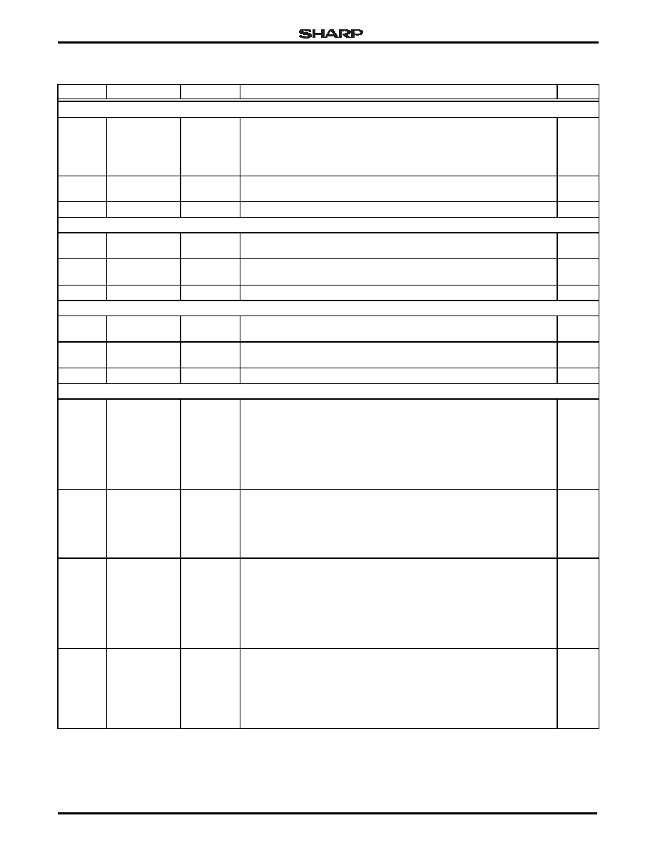
System-on-Chip
LH75400/01/10/11
Preliminary Data Sheet
6/4/03
33
TIMER 0
117
116
115
114
113
CTCAP0[A:E]
Input
Timer 0 Capture Inputs
1
117
116
CTCMP0[A:B]
Output
Timer 0 Compare Outputs
1
118
CTCLK
Input
Common External Clock
1
TIMER 1
111
110
CTCAP1[A:B]
Input
Timer 1 Capture Inputs
1
111
110
CTCMP1[A:B]
Output
Timer 1 Compare Outputs
1
118
CTCLK
Input
Common External Clock
1
TIMER 2
109
108
CTCAP2[A:B]
Input
Timer 2 Capture Inputs
1
109
108
CTCMP2[A:B]
Input
Timer 2 Compare Outputs
1
118
CTCLK
Input
Common External Clock
1
GENERAL PURPOSE INPUT/OUTPUT (GPIO)
1
2
4
5
6
7
9
10
PA7
PA6
PA5
PA4
PA3
PA2
PA1
PA0
Input/Output General Purpose I/O Signals - Port A
1
24
25
27
28
29
30
PB5
PB4
PB3
PB2
PB1
PB0
Input/Output General Purpose I/O Signals - Port B
1
32
33
35
36
37
38
39
40
PC7
PC6
PC5
PC4
PC3
PC2
PC1
PC0
Input/Output General Purpose I/O Signals - Port C
1
72
73
74
76
77
78
79
PD6
PD5
PD4
PD3
PD2
PD1
PD0
Input/Output General Purpose I/O Signals - Port D
1
Table 6. LH75400 Signal Descriptions (Cont'd)
PIN NO. SIGNAL NAME
TYPE
DESCRIPTION
NOTES
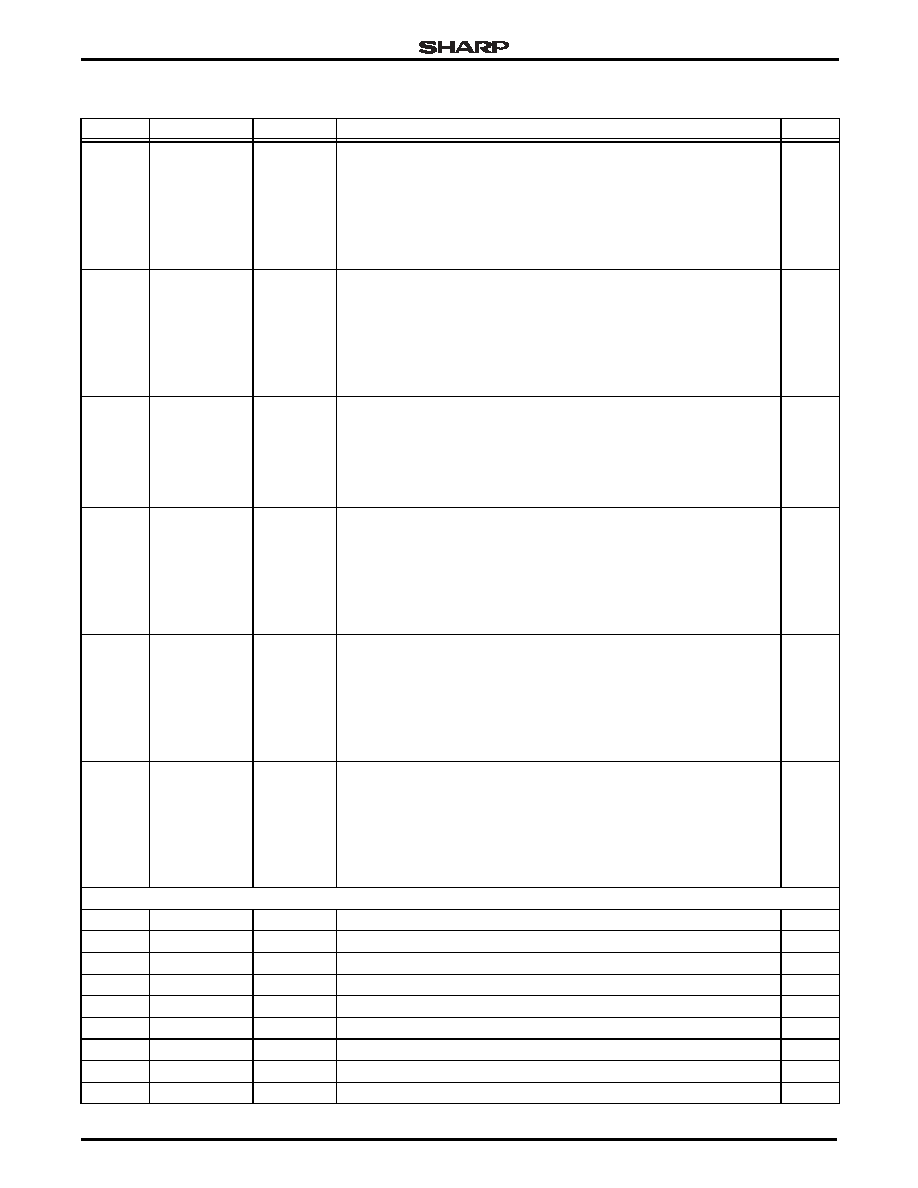
LH75400/01/10/11
System-on-Chip
34
6/4/03
Preliminary Data Sheet
89
90
91
92
93
94
95
96
PJ7
PJ6
PJ5
PJ4
PJ3
PJ2
PJ1
PJ0
Input
General Purpose I/O Signals - Port J
1
99
100
101
102
103
104
105
107
PE7
PE6
PE5
PE4
PE3
PE2
PE1
PE0
Input/Output General Purpose I/O Signals - Port E
1
108
109
110
111
113
114
115
PF6
PF5
PF4
PF3
PF2
PF1
PF0
Input/Output General Purpose I/O Signals - Port F
1
116
117
118
120
121
122
123
124
PG7
PG6
PG5
PG4
PG3
PG2
PG1
PG0
Input/Output General Purpose I/O Signals - Port G
1
125
128
129
130
131
132
133
135
PH7
PH6
PH5
PH4
PH3
PH2
PH1
PH0
Input/Output General Purpose I/O Signals - Port H
1
136
137
138
139
141
142
143
144
PI7
PI6
PI5
PI4
PI3
PI2
PI1
PI0
Input/Output General Purpose I/O Signals - Port I
1
RESET, CLOCK, AND POWER CONTROLLER (RCPC)
62
nRESETIN
Input
User Reset Input
2
71
nRESETOUT
Output
System Reset Output
2
72
INT6
Input
External Interrupt Input 6
1
73
INT5
Input
External Interrupt Input 5
1
74
INT4
Input
External Interrupt Input 4
1
76
INT3
Input
External Interrupt Input 3
1
77
INT2
Input
External Interrupt Input 2
1
78
INT1
Input
External Interrupt Input 1
1
79
INT0
Input
External Interrupt Input 0
1
Table 6. LH75400 Signal Descriptions (Cont'd)
PIN NO. SIGNAL NAME
TYPE
DESCRIPTION
NOTES
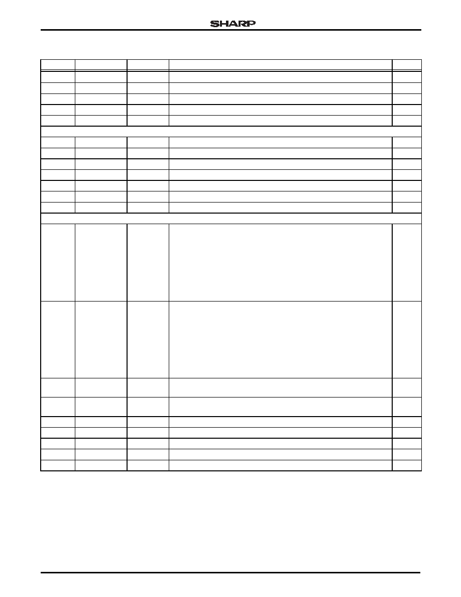
System-on-Chip
LH75400/01/10/11
Preliminary Data Sheet
6/4/03
35
NOTES:
1. These pin numbers have multiplexed functions.
2. Signals preceded with `n' are active LOW.
81
nPOR
Input
Power-on Reset Input
2
82
XTAL32IN
Input
32.768 kHz Crystal Clock Input
83
XTAL32OUT
Output
32.768 kHz Crystal Clock Output
86
XTALIN
Input
Crystal Clock Input
87
XTALOUT
Output
Crystal Clock Output
TEST INTERFACE
63
TEST2
Input
Test Mode Pin 2
64
TEST1
Input
Test Mode Pin 1
65
TMS
Input
JTAG Test Mode Select Input
66
RTCK
Output
Returned JTAG Test Clock Output
67
TCK
Input
JTAG Test Clock Input
68
TDI
Input
JTAG Test Serial Data Input
69
TDO
Output
JTAG Test Data Serial Output
POWER AND GROUND (GND)
3
17
34
42
54
98
112
126
134
VDD
Power
I/O Ring VDD
8
26
41
48
59
106
119
127
140
VSS
Power
I/O Ring VSS
11
75
VDDC
Power
Core VDD supply (Output if Linear Regulator Enabled, Otherwise Input)
14
80
VSSC
Power
Core VSS
70
LINREGEN
Input
Linear Regulator Enable
84
VSSA_PLL
Power
PLL Analog VSS
85
VDDA_PLL
Power
PLL Analog VDD Supply
88
VSSA_ADC
Power
A-to-D converter Analog VSS
97
VDDA_ADC
Power
A-to-D converter Analog VDD Supply
Table 6. LH75400 Signal Descriptions (Cont'd)
PIN NO. SIGNAL NAME
TYPE
DESCRIPTION
NOTES

LH75400/01/10/11
System-on-Chip
36
6/4/03
Preliminary Data Sheet
THE LH75410
Figure 8. LH75410 Pin Diagram
45
44
43
42
41
40
39
38
37
VDD
VSS
PH6/LCDLP
PH5/LCDFP
PH4/LCDEN
PH3/LCDVD11
PH2/LCDVD10
PH1/LCDVD9
VDD
PH0/LCDVD8
PI7/LCDVD7
PI6/LCDVD6
PI5/LCDVD5
PI4/LCDVD4
VSS
PI3/LCDVD3
PI2/LCDVD2
PI1/LCDVD1
PI0/LCDVD0
A4
A5
VDD
A6
A7
A8
A9
A10
VSS
A11
A12
A13
A14
A15
VDD
VSS
PC0/A16
PC1/A17
PC2/A18
PC3/A19
PA7/D15
PA6/D14
VDD
PA5/D13
PA4/D12
PA3/D11
PA2/D10
VSS
PA1/D9
PA0/D8
VDDC
D7
D6
VSSC
D5
D4
VDD
D3
D2
D1
D0
nWE
nOE
PB5/nWAIT
PB4/nBLE1
VSS
PB3/nBLE0
PB2/nCS3
PB1/nCS2
PB0/nCS1
PF6/CTCAP2B/CTCMP2B
PE0/UARTRX2
VSS
PE1/UARTTX2
PE2/UARTRX0
PE3/UARTTX0
PE4/SSPTX
PE5/SSPRX
PE6/SSPCLK
PE7/SSPFRM
VDD
VDDA_ADC
VSSA_ADC
XTALOUT
XTALIN
VDDA_PLL
VSSA_PLL
XTAL32OUT
XTAL32IN
nPOR
VSSC
PD0/INT0
125
126
127
128
129
130
VSS
PG4/LCDVEEEN
PG3/LCDVDDEN
PG2/LCDDSPLEN
PG1
PG0
119
120
121
122
123
124
PF2/CTCAP0E
PF1/CTCAP0D
PF0/CTCAP0C
PG7/CTCAP0B/CTCMP0B
PG6/CTCAP0A/CTCMP0A
PG5/CTCLK
113
114
115
116
117
118
PF5/CTCAP2A/CTCMP2A
PF4/CTCAP1B/CTCMP1B
PF3/CTCAP1A/CTCMP1A
VDD
109
110
111
112
131
132
133
134
135
136
137
138
139
140
141
142
143
144
92
90
89
88
87
86
85
84
83
82
81
80
79
105
104
107
108
106
103
102
101
100
99
98
97
96
94
TOP VIEW
LH75410-51
55
54
53
52
51
50
61
62
60
59
58
57
56
49
48
47
46
nRESETIN
A0
A1
VSS
A2
A3
RTCK
TMS
TEST1
TEST2
65
64
63
71
72
70
69
68
67
66
PD6/INT6/DREQ
nRESETOUT
LINREGEN
TDO
TDI
TCK
144-PIN LQFP
1
2
3
4
5
6
7
8
9
10
11
12
13
14
15
16
17
18
19
20
21
22
23
24
25
26
27
28
29
30
nCS0
PC7/A23
PC6/A22
VDD
PC5/A21
PC4/A20
31
32
33
34
35
36
PD1/INT1
PD2/INT2
PD3/INT3/UARTTX1
VDDC
PD4/INT4/UARTRX1
PD5/INT5/DACK
78
77
76
75
74
73
PH7/LCDDCLK
AN0(UL
/
X+)/PJ0
AN1(UR
/
X-)/PJ2
AN2(LL
/
Y+)/PJ4
AN4(WIPER)/PJ6
AN3(LR
/
Y-)/PJ7
AN6/PJ1
AN8/PJ3
AN9/PJ5
91
95
93
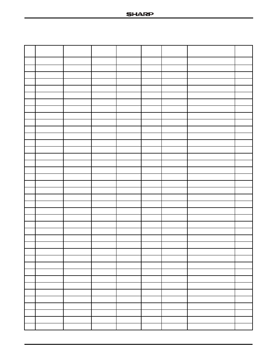
System-on-Chip
LH75400/01/10/11
Preliminary Data Sheet
6/4/03
37
LH75410 Numerical Pin Listing
Table 7. LH75410 Numerical Pin List
PIN
NO.
FUNCTION
AT RESET
FUNCTION
2
FUNCTION
3
FUNCTION
TYPE
OUTPUT
DRIVE
BUFFER
TYPE
PULL-UP/PULL-DOWN
AT RESET
NOTES
1
PA7
D15
I/O
8 mA
Bidirectional
1
2
PA6
D14
I/O
8 mA
Bidirectional
1
3
VDD
Power
None
4
PA5
D13
I/O
8 mA
Bidirectional
1
5
PA4
D12
I/O
8 mA
Bidirectional
1
6
PA3
D11
I/O
8 mA
Bidirectional
1
7
PA2
D10
I/O
8 mA
Bidirectional
1
8
VSS
Ground
None
9
PA1
D9
I/O
8 mA
Bidirectional
1
10
PA0
D8
I/O
8 mA
Bidirectional
1
11
VDDC
Power
None
12
D7
I/O
8 mA
Bidirectional
13
D6
I/O
8 mA
Bidirectional
14
VSSC
Ground
None
15
D5
I/O
8 mA
Bidirectional
16
D4
I/O
8 mA
Bidirectional
17
VDD
Power
None
18
D3
I/O
8 mA
Bidirectional
19
D2
I/O
8 mA
Bidirectional
20
D1
I/O
8 mA
Bidirectional
21
D0
I/O
8 mA
Bidirectional
22
nWE
8 mA
Output
3
23
nOE
8 mA
Output
3
24
PB5
nWAIT
8 mA
Bidirectional
Pull-up
1
25
PB4
nBLE1
8 mA
Bidirectional
Pull-up
1
26
VSS
Ground
None
27
PB3
nBLE0
8 mA
Bidirectional
Pull-up
1
28
PB2
nCS3
8 mA
Bidirectional
Pull-up
1
29
PB1
nCS2
8 mA
Bidirectional
Pull-up
1
30
PB0
nCS1
8 mA
Bidirectional
Pull-up
1
31
nCS0
8 mA
Output
3
32
PC7
A23
8 mA
Bidirectional
Pull-down
1
33
PC6
A22
8 mA
Bidirectional
Pull-down
1
34
VDD
Power
None
35
PC5
A21
8 mA
Bidirectional
Pull-down
1
36
PC4
A20
8 mA
Bidirectional
Pull-down
1
37
PC3
A19
8 mA
Bidirectional
Pull-down
1
38
PC2
A18
8 mA
Bidirectional
Pull-down
1
39
PC1
A17
8 mA
Bidirectional
Pull-down
1
40
PC0
A16
8 mA
Bidirectional
Pull-down
1
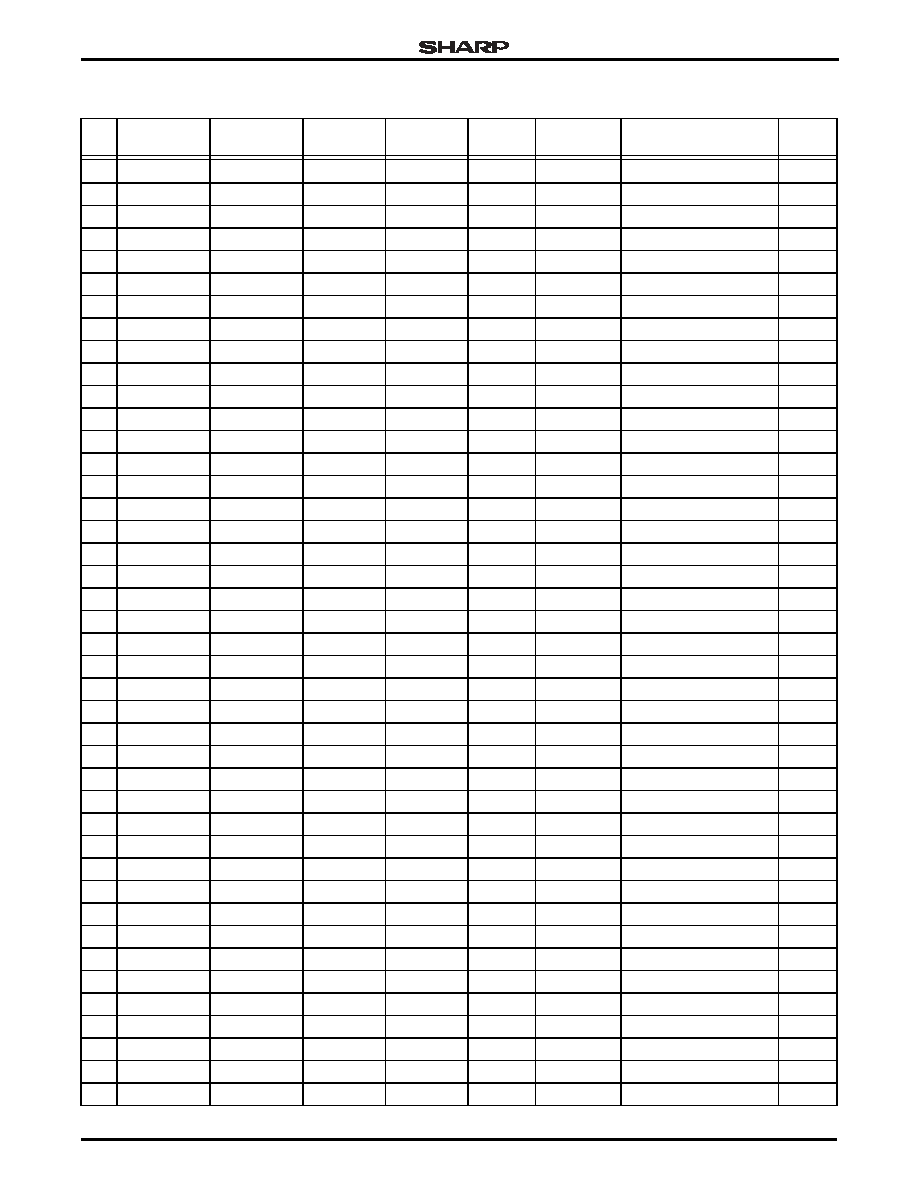
LH75400/01/10/11
System-on-Chip
38
6/4/03
Preliminary Data Sheet
41
VSS
Ground
None
42
VDD
Power
None
43
A15
8 mA
Output
44
A14
8 mA
Output
45
A13
8 mA
Output
46
A12
8 mA
Output
47
A11
8 mA
Output
48
VSS
Ground
None
49
A10
8 mA
Output
50
A9
8 mA
Output
51
A8
8 mA
Output
52
A7
8 mA
Output
53
A6
8 mA
Output
54
VDD
Power
None
55
A5
8 mA
Output
56
A4
8 mA
Output
57
A3
8 mA
Output
58
A2
8 mA
Output
59
VSS
Ground
None
60
A1
8 mA
Output
61
A0
8 mA
Output
62
nRESETIN
None
Input
Pull-up
2, 3
63
TEST2
None
Input
Pull-up
2
64
TEST1
None
Input
Pull-up
2
65
TMS
None
Input
Pull-up
2
66
RTCK
4 mA
Output
67
TCK
None
Input
68
TDI
None
Input
Pull-up
2
69
TDO
4 mA
Output
70
LINREGEN
None
Input
71
nRESETOUT
8 mA
Output
3
72
PD6
INT6
DREQ
6 mA
Bidirectional
Pull-down
1
73
PD5
INT5
DACK
6 mA
Bidirectional
1, 2
74
PD4
INT4
UARTRX1
8 mA
Bidirectional
Pull-up
1
75
VDDC
Power
None
76
PD3
INT3
UARTTX1
8 mA
Bidirectional
Pull-up
1
77
PD2
INT2
2 mA
Bidirectional
Pull-up
1
78
PD1
INT1
6 mA
Bidirectional
1, 2
79
PD0
INT0
2 mA
Bidirectional
1
80
VSSC
Ground
None
81
nPOR
None
Input
Pull-up
2, 3
82
XTAL32IN
None
Output
Table 7. LH75410 Numerical Pin List (Cont'd)
PIN
NO.
FUNCTION
AT RESET
FUNCTION
2
FUNCTION
3
FUNCTION
TYPE
OUTPUT
DRIVE
BUFFER
TYPE
PULL-UP/PULL-DOWN
AT RESET
NOTES

System-on-Chip
LH75400/01/10/11
Preliminary Data Sheet
6/4/03
39
83
XTAL32OUT
None
Output
84
VSSA_PLL
Ground
None
85
VDDA_PLL
Power
None
86
XTALIN
None
Input
87
XTALOUT
None
Output
88
VSSA_ADC
Ground
None
89
AN3 (LR/Y-)
PJ7
None
Input
90
AN4 (Wiper)
PJ6
None
Input
91
AN9 PJ5
None
Input
92
AN2 (LL/Y+)
PJ4
None
Input
93
AN8 PJ3
None
Input
94
AN1 (UR/X-)
PJ2
None
Input
95
AN6 PJ1
None
Input
96
AN0 (UL/X+)
PJ0
None
Input
97
VDDA_ADC
Power
None
98
VDD
Power
None
99
PE7
SSPFRM
4 mA
Bidirectional
Pull-up
1
100
PE6
SSPCLK
4 mA
Bidirectional
Pull-down
1
101
PE5
SSPRX
4 mA
Bidirectional
Pull-up
1
102
PE4
SSPTX
4 mA
Bidirectional
Pull-down
1
103
PE3
UARTTX0
8 mA
Bidirectional
Pull-up
1
104
PE2
UARTRX0
2 mA
Bidirectional
Pull-up
1
105
PE1
UARTTX2
4 mA
Bidirectional
Pull-up
1
106
VSS
Ground
None
107
PE0
UARTRX2
4 mA
Bidirectional
Pull-up
1
108
PF6
CTCAP2B
CTCMP2B
4 mA
Bidirectional
2
109
PF5
CTCAP2A
CTCMP2A
4 mA
Bidirectional
110
PF4
CTCAP1B
CACMP1B
4 mA
Bidirectional
2
111
PF3
CTCAP1A
CTCMP1A
4 mA
Bidirectional
112
VDD
Power
None
113
PF2
CTCAP0E
4 mA
Bidirectional
2
114
PF1
CTCAP0D
4 mA
Bidirectional
115
PF0
CTCAP0C
4 mA
Bidirectional
2
116
PG7
CTCAP0B
CTCMP0B
4 mA
Bidirectional
117
PG6
CTCAP0A
CTCMP0A
4 mA
Bidirectional
2
118
PG5
CTCLK
4 mA
Bidirectional
119
VSS
Ground
None
120
PG4
LCDVEEEN
8 mA
Bidirectional
121
PG3
LCDVDDEN
8 mA
Bidirectional
122
PG2
LCDDSPLEN
8 mA
Bidirectional
123
PG1
8 mA
Bidirectional
124
PG0
8 mA
Bidirectional
Table 7. LH75410 Numerical Pin List (Cont'd)
PIN
NO.
FUNCTION
AT RESET
FUNCTION
2
FUNCTION
3
FUNCTION
TYPE
OUTPUT
DRIVE
BUFFER
TYPE
PULL-UP/PULL-DOWN
AT RESET
NOTES

LH75400/01/10/11
System-on-Chip
40
6/4/03
Preliminary Data Sheet
NOTES:
1. Signal is selectable as pull-up, pull-down, or no pull-up/pull-down via the I/O Configuration peripheral.
2. CMOS Schmitt trigger input.
3. Signals preceded with `n' are active LOW.
125
PH7
LCDDCLK
8 mA
Bidirectional
126
VDD
Power
None
127
VSS
Ground
None
128
PH6
LCDLP
8 mA
Bidirectional
129
PH5
LCDFP
8 mA
Bidirectional
130
PH4
LCDEN
8 mA
Bidirectional
131
PH3
LCDVD11
8 mA
Bidirectional
132
PH2
LCDVD10
8 mA
Bidirectional
133
PH1
LCDVD9
8 mA
Bidirectional
134
VDD
Power
None
135
PH0
LCDVD8
8 mA
Bidirectional
136
PI7
LCDVD7
8 mA
Bidirectional
137
PI6
LCDVD6
8 mA
Bidirectional
138
PI5
LCDVD5
8 mA
Bidirectional
139
PI4
LCDVD4
8 mA
Bidirectional
140
VSS
Ground
None
141
PI3
LCDVD3
8 mA
Bidirectional
142
PI2
LCDVD2
8 mA
Bidirectional
143
PI1
LCDVD1
8 mA
Bidirectional
144
PI0
LCDVD0
8 mA
Bidirectional
Table 7. LH75410 Numerical Pin List (Cont'd)
PIN
NO.
FUNCTION
AT RESET
FUNCTION
2
FUNCTION
3
FUNCTION
TYPE
OUTPUT
DRIVE
BUFFER
TYPE
PULL-UP/PULL-DOWN
AT RESET
NOTES
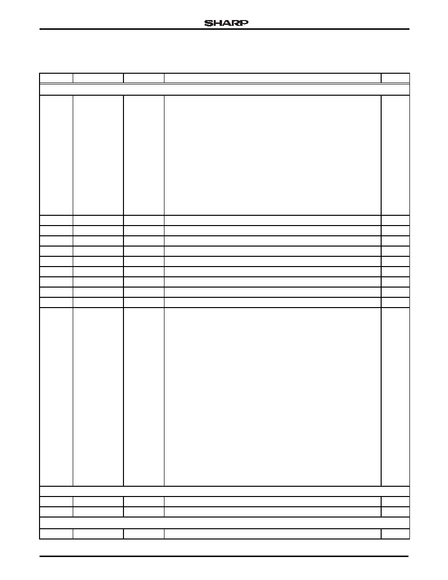
System-on-Chip
LH75400/01/10/11
Preliminary Data Sheet
6/4/03
41
LH75410 Signal Descriptions
Table 8. LH75410 Signal Descriptions
PIN NO. SIGNAL NAME
TYPE
DESCRIPTION
NOTES
MEMORY INTERFACE (MI)
1
2
4
5
6
7
9
10
12
13
15
16
18
19
20
21
D[15:0]
Input/Output Data Input/Output Signals
1
22
nWE
Output
Static Memory Controller Write Enable
2
23
nOE
Output
Static Memory Controller Output Enable
2
24
nWAIT
Input
Static Memory Controller External Wait Control
1, 2
25
nBLE1
Output
Static Memory Controller Byte Lane Strobe
1, 2
27
nBLE0
Output
Static Memory Controller Byte Lane Strobe
1, 2
28
nCS3
Output
Static Memory Controller Chip Select
1, 2
29
nCS2
Output
Static Memory Controller Chip Select
1, 2
30
nCS1
Output
Static Memory Controller Chip Select
1, 2
31
nCS0
Output
Static Memory Controller Chip Select
2
32
33
35
36
37
38
39
40
43
44
45
46
47
49
50
51
52
53
55
56
57
58
60
61
A[23:0]
Output
Address Signals
1
DMA CONTROLLER (DMAC)
72
DREQ
Input
DMA Request
1
73
DACK
Output
DMA Acknowledge
1
LCD CONTROLLER (LCDC)
120
LCDVEEEN
Output
Analog Supply Enable (AC Bias SIgnal)
1

LH75400/01/10/11
System-on-Chip
42
6/4/03
Preliminary Data Sheet
121
LCDVDDEN
Output
Digital Supply Enable
1
122
LCDDSPLEN
Output
LCD Panel Power Enable
1
125
LCDDCLK
Output
LCD Panel Clock
1
128
LCDLP
Output
Line Synchronization Pulse (STN), Horizontal Synchronization Pulse (TFT)
1
129
LCDFP
Output
Frame Pulse (STN), Vertical Synchronization Pulse (TFT)
1
130
LCDEN
Output
LCD Data Enable
1
131
132
133
135
136
137
138
139
141
142
143
144
LCDVD[11:0]
Output
LCD Panel Data bus
1
SYNCHRONOUS SERIAL PORT (SSP)
99
SSPFRM
Input
SSP Serial Frame
1
100
SSPCLK
Input
SSP Clock
1
101
SSPRX
Input
SSP RXD
1
102
SSPTX
Output
SSP TXD
1
UART0 (U0)
103
UARTTX0
Output
UART0 Transmitted Serial Data Output
1
104
UARTRX0
Input
UART0 Received Serial Data Input
1
UART1 (U1)
74
UARTRX1
Input
UART1 Received Serial Data Input
1
76
UARTTX1
Output
UART1 Transmitted Serial Data Output
1
UART2 (U2)
105
UARTTX2
Output
UART2 Transmitted Serial Data Output
1
107
UARTRX2
Input
UART2 Received Serial Data Input
1
ANALOG-TO-DIGITAL CONVERTER (ADC)
89
90
91
92
93
94
95
96
AN3 (LR/Y-)
AN4 (Wiper)
AN9
AN2 (LL/Y+)
AN8
AN1 (UR/X-)
AN6
AN0 (UL/X+)
Input
ADC Inputs
1
TIMER 0
117
116
115
114
113
CTCAP0[A:E]
Input
Timer 0 Capture Inputs
1
117
116
CTCMP0[A:B]
Output
Timer 0 Compare Outputs
1
118
CTCLK
Input
Common External Clock
1
Table 8. LH75410 Signal Descriptions (Cont'd)
PIN NO. SIGNAL NAME
TYPE
DESCRIPTION
NOTES
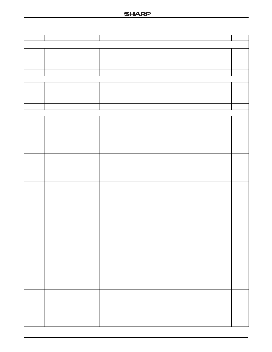
System-on-Chip
LH75400/01/10/11
Preliminary Data Sheet
6/4/03
43
TIMER 1
111
110
CTCAP1[A:B]
Input
Timer 1 Capture Inputs
1
111
110
CTCMP1[A:B]
Output
Timer 1 Compare Outputs
1
118
CTCLK
Input
Common External Clock
1
TIMER 2
109
108
CTCAP2[A:B]
Input
Timer 2 Capture Inputs
1
109
108
CTCMP2[A:B]
Input
Timer 2 Compare Outputs
1
118
CTCLK
Input
Common External Clock
1
GENERAL PURPOSE INPUT/OUTPUT (GPIO)
1
2
4
5
6
7
9
10
PA7
PA6
PA5
PA4
PA3
PA2
PA1
PA0
Input/Output General Purpose I/O Signals - Port A
1
24
25
27
28
29
30
PB5
PB4
PB3
PB2
PB1
PB0
Input/Output General Purpose I/O Signals - Port B
1
32
33
35
36
37
38
39
40
PC7
PC6
PC5
PC4
PC3
PC2
PC1
PC0
Input/Output General Purpose I/O Signals - Port C
1
72
73
74
76
77
78
79
PD6
PD5
PD4
PD3
PD2
PD1
PD0
Input/Output General Purpose I/O Signals - Port D
1
89
90
91
92
93
94
95
96
PJ7
PJ6
PJ5
PJ4
PJ3
PJ2
PJ1
PJ0
Input
General Purpose I/O Signals - Port J
1
99
100
101
102
103
104
105
107
PE7
PE6
PE5
PE4
PE3
PE2
PE1
PE0
Input/Output General Purpose I/O Signals - Port E
1
Table 8. LH75410 Signal Descriptions (Cont'd)
PIN NO. SIGNAL NAME
TYPE
DESCRIPTION
NOTES
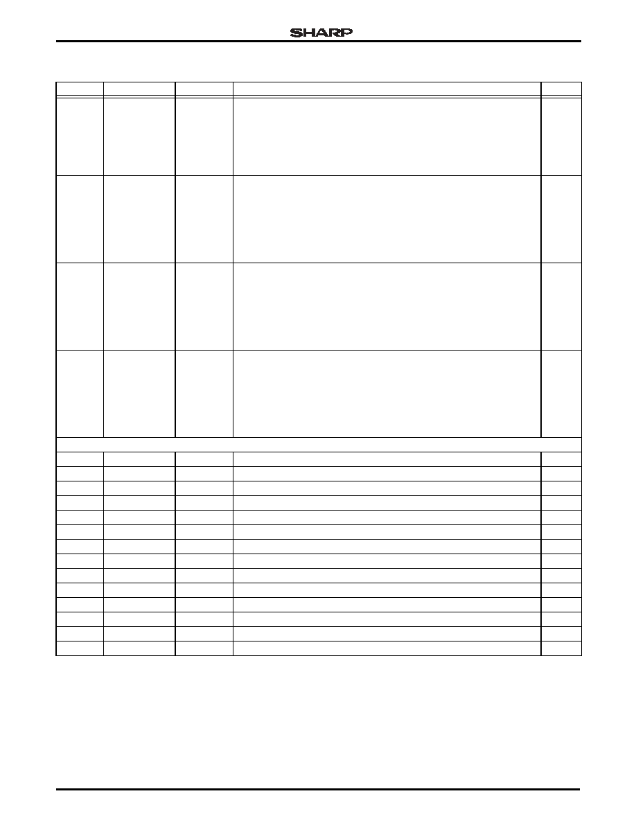
LH75400/01/10/11
System-on-Chip
44
6/4/03
Preliminary Data Sheet
108
109
110
111
113
114
115
PF6
PF5
PF4
PF3
PF2
PF1
PF0
Input/Output General Purpose I/O Signals - Port F
1
116
117
118
120
121
122
123
124
PG7
PG6
PG5
PG4
PG3
PG2
PG1
PG0
Input/Output General Purpose I/O Signals - Port G
1
125
128
129
130
131
132
133
135
PH7
PH6
PH5
PH4
PH3
PH2
PH1
PH0
Input/Output General Purpose I/O Signals - Port H
1
136
137
138
139
141
142
143
144
PI7
PI6
PI5
PI4
PI3
PI2
PI1
PI0
Input/Output General Purpose I/O Signals - Port I
1
RESET, CLOCK, AND POWER CONTROLLER (RCPC)
62
nRESETIN
Input
User Reset Input
2
71
nRESETOUT
Output
System Reset Output
2
72
INT6
Input
External Interrupt Input 6
1
73
INT5
Input
External Interrupt Input 5
1
74
INT4
Input
External Interrupt Input 4
1
76
INT3
Input
External Interrupt Input 3
1
77
INT2
Input
External Interrupt Input 2
1
78
INT1
Input
External Interrupt Input 1
1
79
INT0
Input
External Interrupt Input 0
1
81
nPOR
Input
Power-on Reset Input
2
82
XTAL32IN
Input
32.768 kHz Crystal Clock Input
83
XTAL32OUT
Output
32.768 kHz Crystal Clock Output
86
XTALIN
Input
Crystal Clock Input
87
XTALOUT
Output
Crystal Clock Output
Table 8. LH75410 Signal Descriptions (Cont'd)
PIN NO. SIGNAL NAME
TYPE
DESCRIPTION
NOTES
System-on-Chip
LH75400/01/10/11
Preliminary Data Sheet
6/4/03
45
NOTES:
1. These pins have multiplexed functions.
2. Signals preceded with `n' are active LOW.
TEST INTERFACE
63
TEST2
Input
Test Mode Pin 2
64
TEST1
Input
Test Mode Pin 1
65
TMS
Input
JTAG Test Mode Select Input
66
RTCK
Output
Returned JTAG Test Clock Output
67
TCK
Input
JTAG Test Clock Input
68
TDI
Input
JTAG Test Serial Data Input
69
TDO
Output
JTAG Test Data Serial Output
POWER AND GROUND (GND)
3
17
34
42
54
98
112
126
134
VDD
Power
I/O Ring VDD
8
26
41
48
59
106
119
127
140
VSS
Power
I/O Ring VSS
11
75
VDDC
Power
Core VDD supply (Output if Linear Regulator Enabled, Otherwise Input)
14
80
VSSC
Power
Core VSS
70
LINREGEN
Input
Linear Regulator Enable
84
VSSA_PLL
Power
PLL Analog VSS
85
VDDA_PLL
Power
PLL Analog VDD Supply
88
VSSA_ADC
Power
A-to-D converter Analog VSS
97
VDDA_ADC
Power
A-to-D converter Analog VDD Supply
Table 8. LH75410 Signal Descriptions (Cont'd)
PIN NO. SIGNAL NAME
TYPE
DESCRIPTION
NOTES
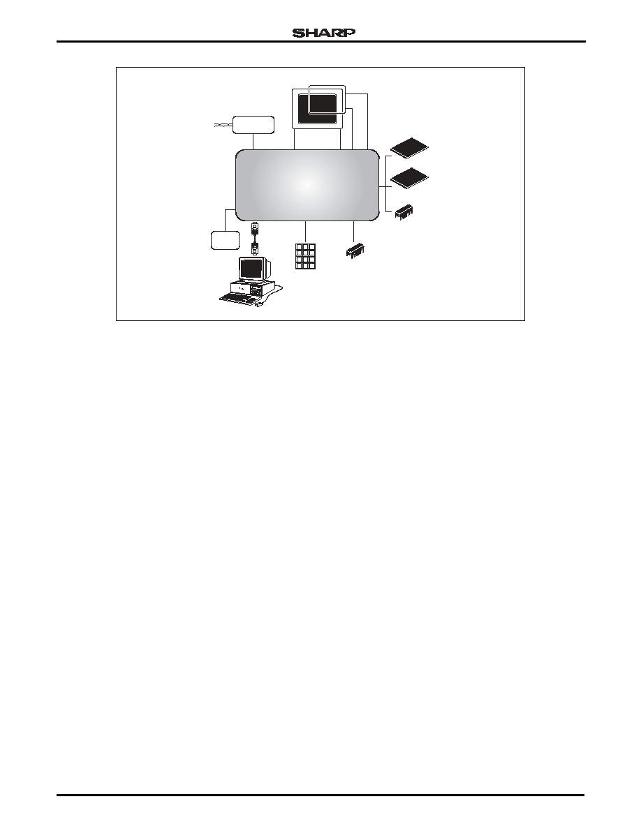
LH75400/01/10/11
System-on-Chip
46
6/4/03
Preliminary Data Sheet
FUNCTIONAL OVERVIEW
ARM7TDMI-S Processor
The LH75400/01/10/11 microcontrollers feature the
A R M 7 T D M I - S c o r e w i t h a n A d v a n c e d H i g h -
P e r f o r m a n c e B u s ( A H B ) 2 . 0 i n t e r f a c e . T h e
ARM7TDMI-S is a 16/32-bit embedded RISC proces-
sor and a member of the ARM7 Thumb family of pro-
cessors. For more information, visit the ARM Web site
at www.arm.com.
Bus Architecture
The LH75400/01/10/11 microcontrollers use the
ARM Advanced Microcontroller Bus Architecture (AMBA)
2.0 internal bus protocol. Three AHB masters control
access to external memory and on-chip peripherals:
∑ The ARM processor fetches instructions and trans-
fers data
∑ The Direct Memory Access Controller (DMAC) trans-
fers from memory to memory, from peripheral to
memory, and from memory to peripheral
∑ The LCDC refreshes an LCD panel with data from
the external memory or from internal memory if the
frame buffer is 16KB or less.
The ARM7TDMI-S processor is the default bus mas-
ter. An Advanced Peripheral Bus (APB) bridge is pro-
vided to access to the various APB peripherals.
Generally, APB peripherals are serviced by the ARM
core. However, if they are DMA-enabled, they are also
serviced by the DMAC to increase system performance
while the ARM core runs from local internal memory.
Power Supplies
Five-Volt-tolerant 3.3 V I/Os are employed. The
LH75400/01/10/11 microcontrollers require a single
3.3 V supply. The core logic requires a 1.8 V supply. A
linear regulator integrated into the chip generates the
1.8 V for the core logic.
Crystal Oscillators
The LH75400/01/10/11 microcontrollers provide for
two crystal oscillators.
∑ One drives an internal Phase Lock Loop (PLL) and
the three UARTs. It supports a frequency range from
14 MHz to 20 MHz and requires a 1.8 V source on its
external inputs.
∑ Another is a 32.768 kHz oscillator that generates a
1 Hz clock for the RTC.
Although the internal PLL's input frequency range is
from 14 MHz to 40 MHz, the crystal oscillator limits the
useful range to 14 MHz to 20 MHz. The resulting output
frequency range is 98 MHz to 140 MHz.
The frequency ranges of the PLL and crystal oscillator
together provide a crystal frequency range of operation
from 14 MHz to 20 MHz. However, since the crystal
oscillator drives the UART clocks, an oscillator frequency
of 14.7456 MHz is recommended (but not required). This
frequency can be divided-down to exact frequencies that
a UART needs to achieve modem baud rates. This cre-
ates a PLL output frequency of approximately
103.2192 MHz. The system clock frequency can be from
divide-by-30 to divide-by-2 (3.44 MHz to 51.6096 MHz
using a 14.7456 MHz crystal) in decrements of two (30,
28, 26, 24, and so on) of the PLL frequency.
Figure 9. LH75401 System Application Example
STN/TFT,
AD-TFT/HR-TFT
LCD
TOUCH SCREEN
GPIO
SSP
A/D
KEY
MATRIX
SERIAL
EEPROM
CAN
2.0B
CAN
NETWORK
A/D
FLASH
SRAM
BOOT
ROM
UART
LH75401
CAN
TRANSCEIVER
SENSOR
ARRAY
LH754xx-2A
1
2
3
4
5
6
7
8
9
*
0
#

System-on-Chip
LH75400/01/10/11
Preliminary Data Sheet
6/4/03
47
Reset Generation
EXTERNAL RESETS
Two external signals generate resets to the
ARM7TDMI-S core:
∑ nPOR sets all internal registers to their default state
when asserted. It is used as a Power-On Reset.
∑ nRESETIN sets all internal registers, except the
JTAG circuitry, to their default state when asserted.
When nPOR is asserted, nRESETIN defines the
microcontroller Test Mode. When nPOR is released,
nRESETIN behaves during Reset as described
previously.
INTERNAL RESETS
There are two types of Internal Resets generated:
∑ System Reset
∑ RTC Reset.
System and RTC Resets are asserted by:
∑ An External Reset (a logic LOW signal on the exter-
nal nRESETIN or nPOR input pin)
∑ A signal from the internal Watchdog Timer
∑ A Soft Reset.
The reset latency depends on the PLL lock state.
AHB Master Priority and Arbitration
The LH75400/01/10/11 microcontrollers have three
AHB masters:
∑ ARM processor
∑ DMAC
∑ LCD Controller.
Each AHB master has a priority level that is perma-
nent and cannot change.
Memory Interface Architecture
The LH75400/01/10/11 microcontrollers provide the
following data-path management resources on chip:
∑ AHB and APB data buses
∑ 16KB of zero-wait-state TCM SRAM accessible via
processor
∑ 16KB of internal SRAM accessible via processor,
DMAC, and LCDC
∑ A Static Memory Controller (SMC) that controls
access to external memory
∑ A 4-stream general-purpose DMAC.
All external and internal system resources are
memory-mapped. This memory map partition has three
views, based on the setting of the REMAP bits in the
Reset, Clock, and Power Controller (RCPC).
The second partitioning of memory space is the
dividing of the segments into sections. The external
memory segment is divided into eight 64MB sections,
of which the first four are used, each having a chip
select associated with it. Access to any of the last four
sections does not result in an external bus access and
does not cause a memory abort. The peripheral regis-
ter segment is divided into 4KB peripheral sections, 21
of which are assigned to peripherals.
Table 9. Bus Master Priority
PRIORITY
BUS MASTER PRIORITY
1 (Highest)
Color LCDC (LH75401 and LH75411)
LCDC (LH75400 and LH75410)
2
DMAC
3 (Lowest)
ARM7TDMI-S Core (Default)
Table 10. Memory Mapping
ADDRESS
REMAP = 00
(DEFAULT)
REMAP = 01 REMAP = 10
0x00000000
External
Memory
Internal
SRAM
TCM SRAM
0x20000000
Reserved
Reserved
Reserved
0x40000000
External
Memory
External
Memory
External
Memory
0x60000000
Internal
SRAM
Internal
SRAM
Internal
SRAM
0x80000000
TCM SRAM
TCM SRAM
TCM SRAM
0xA0000000
Reserved
Reserved
Reserved
0xC0000000
Reserved
Reserved
Reserved
0xE0000000 -
0xFFFBFFFF
Reserved
Reserved
Reserved
LH75400/01/10/11
System-on-Chip
48
6/4/03
Preliminary Data Sheet
Static Random Access Memory Controller
The LH75400/01/10/11 microcontrollers have 32KB
of Static Random Access Memory (SRAM) organized
into two 16KB blocks:
∑ 16KB of TCM 0 Wait State SRAM is available to the
processor as an ARM7TDMI-S bus slave.
∑ 16KB of internal SRAM is available as an AHB slave
and accessible via processor, DMAC, and LCDC.
Each memory segment is 512MB, though the TCM
and internal SRAMs are 16KB each in size. Any access
beyond the first 16KB is mapped to the lower 16KB, but
does not cause a data or prefetch abort.
Static Memory Controller (SMC)
The Static Memory Controller (SMC) is an AMBA
AHB slave peripheral that provides the interface
between the LH75400/01/10/11 microcontrollers and
external memory devices.
SMC FEATURES
∑ Provides four banks of external memory, each with a
maximum size of 16MB.
∑ Supports memory-mapped devices, including
Random Access Memory (RAM), Read Only
Memory (ROM), Flash, and burst ROM
∑ Supports external bus and external device widths of
8 and 16 bits
∑ Supports Asynchronous Burst Mode read access for
Burst Mode ROM devices, with up to 32 independent
wait states for read and write accesses
∑ Supports indefinite extended wait states via an
external hardware pin (nWAIT)
∑ Supports varied bus turnaround cycles (1 to 16)
between a read and write operation
Direct Memory Access Controller (DMAC)
One central DMAC services all peripheral DMA
requirements for the DMA-capable peripherals listed in
Table 12.
The DMA is controlled by the system clock. It has an
APB slave port for programming of its registers and an
AHB port for data transfers.
DMAC FEATURES
∑ Four data streams that can be used to service:
≠ Four peripheral data streams (peripheral-to-
memory or memory-to-peripheral)
≠ Three peripheral data streams and one memory-
to-memory data stream.
∑ Three transfer modes:
≠ Memory to Memory (selectable on Stream3)
≠ Peripheral to Memory (all streams)
≠ Memory to Peripheral (all streams).
∑ Built-in data stream arbiter
∑ Seven programmable registers for each stream
∑ Ability for each stream to indicate a transfer error via
an interrupt
∑ 16-word First-In, First Out (FIFO) array, with pack
and unpack logic to handle all input/output combina-
tions of byte, half-word, and word transfers
∑ APB slave port allows the ARM core to program
DMAC registers
∑ AHB port for data transfers.
Table 11. APB Peripheral Register Mapping
ADDRESS RANGE
DEVICE
0xFFFC0000 - 0xFFFC0FFF UART0 (16550)
0xFFFC1000 - 0xFFFC1FFF UART1 (16550)
0xFFFC2000 - 0xFFFC2FFF UART2 (82510)
0xFFFC3000 - 0xFFFC3FFF Analog-to-Digital Converter
0xFFFC4000 - 0xFFFC4FFF Timer Module
0xFFFC5000 - 0xFFFC5FFF
CAN (LH75401/LH75400)
Reserved (LH75411/LH75410)
0xFFFC6000 - 0xFFFC6FFF Synchronous Serial Port
0xFFFC7000 - 0xFFFDAFFF Reserved
0xFFFDB000 - 0xFFFDBFFF GPIO4
0xFFFDC000 - 0xFFFDCFFF GPIO3
0xFFFDD000 - 0xFFFDDFFF GPIO2
0xFFFDE000 - 0xFFFDEFFF GPIO1
0xFFFDF000 - 0xFFFDFFFF GPIO0
0xFFFE0000 - 0xFFFE0FFF Real Time Clock
0xFFFE1000 - 0xFFFE1FFF DMAC
0xFFFE2000 - 0xFFFE2FFF
Reset Clock and Power
Controller
0xFFFE3000 - 0xFFFE3FFF Watchdog Timer
0xFFFE4000 - 0xFFFE4FFF LCD ICP (HR-TFT support)
0xFFFE5000 - 0xFFFE5FFF I/O Configuration Peripheral
0xFFFE6000 - 0xFFFEFFFF Reserved
Table 12. DMAC Stream Assignments
DMA REQUEST SOURCE
DMA STREAM
UART1RX (highest priority)
Stream0
UART1TX
Stream1
UART0RX/External Request (DREQ)
Stream2
UART0TX (lowest priority)
Stream3

System-on-Chip
LH75400/01/10/11
Preliminary Data Sheet
6/4/03
49
Color LCD Controller (CLCDC)
The CLCDC is an AMBA master-slave module that
connects to the AHB. It translates pixel-coded data into
the required formats and timings to drive single/dual
monochrome and color LCD panels. Packets of pixel-
coded data are fed, via the AHB interface, to two inde-
pendently programmable, 32-bit-wide DMA FIFOs.
Each FIFO is 16 words deep by 32 bits wide.
The CLCDC generates a single combined interrupt
to the Vectored Interrupt Controller (VIC) when an
interrupt condition becomes true for upper/lower panel
DMA FIFO underflow, base address update significa-
tion, vertical compare, or bus error.
NOTE:
LH75401 and LH75411 microcontrollers support full-color
operation. LH75400 and LH75410 microcontrollers are
monochrome only.
CLCDC FEATURES
∑ STN, Color STN, TFT, HR-TFT, and AD-TFT
≠ Fully Programmable Timing Controls
≠ Integrated Controller for displays with a low level
of integration, such as HR-TFT and AD-TFT
∑ Programmable Resolution
≠ Up to VGA (640 ◊ 480 DPI), 12-bit Direct Mode
Color
≠ Up to SVGA (800 ◊ 600 DPI), 8-bit Direct/Paletized
Color
≠ Up to XGA (1,024 ◊ 768 DPI), 4-bit Direct Color/
Grayscale
≠ Direct or Paletized Colors
∑ Single and Dual Panels
∑ Supports Sharp and non-Sharp Panels
∑ CLCDC Outputs Available as General Purpose
Inputs/Outputs (GPIOs) if LCDC is Not Needed
∑ Additional Features
≠ Fully programmable horizontal and vertical timing
for different display panels
≠ 256-entry, 16-bit palette RAM physically arranged
as a 128 ◊ 32-bit RAM
≠ AC bias signal for STN panels and a data-enable
signal for TFT panels.
∑ Programmable Panel-related Parameters
≠ STN mono/color or TFT display
≠ Bits-per-pixel
≠ STN 4- or 8-bit Interface Mode
≠ STN Dual or Single Panel Mode
≠ AC panel bias
≠ Panel clock frequency
≠ Number of panel clocks per line
≠ Signal polarity, active HIGH or LOW
≠ Little Endian data format
≠ Interrupt-generation event.
HR-TFT/AD-TFT Controller
(HRTFTC/AD-TFT)
The HRTFTC/ADTFTC is used with the CLCDC and
accessed via the AMBA APB interface.
The HRTFTC/ADTFTC is supplied with the standard
TFT output from the LCDC and produces the neces-
sary control and data signals to interface to an HR-TFT/
AD-TFT-type display.
The HRTFTC/ADTFTC has two operating modes:
∑ Bypass Mode where input signals from the CLCDC
pass directly to the output pins, without any signal
reformatting. This is the default mode.
∑ HR-TFT/AD-TFT Mode for driving an HR-TFT/
AD-TFT display.
NOTES:The HR-TFT/AD-TFT controller pertains to the LH75401
and LH75411 microcontrollers.
VGA and XGA modes require 66 MHz core speed.
Universal Asynchronous
Receiver Transmitters (UARTs)
The LH75400/01/10/11 microcontrollers incorporate
three UARTs, designated UART0, UART1, and
UART2.
UART 0 AND 1 FEATURES
∑ Similar functionality to the industry-standard 16C550
∑ Supported baud rates up to 921,600 baud (given an
external crystal frequency of 14.756 MHz)
∑ Supported character formats:
≠ Data bits per character: 5, 6, 7, or 8
≠ Parity generation and detection: Even, odd, stick,
or none
≠ Stop bit generation: 1 or 2
∑ Full-duplex operation
∑ Separate transmit and receive FIFOs, with:
≠ Programmable depth (1 to 16)
≠ Programmable-service `trigger levels' (1/8, 1/4,
1/2, 3/4, and 7/8)
≠ Overrun protection.
∑ Programmable baud-rate generator that:
≠ Enables the UART input clock to be divided by 16
to 65,535 ◊ 16
≠ Generates an internal clock common to both
transmit and receive portions of the UART.
∑ DMA support
∑ Support for generating and detecting breaks during
UART transactions
∑ Loopback testing.

LH75400/01/10/11
System-on-Chip
50
6/4/03
Preliminary Data Sheet
UART 2 FEATURES
∑ Similar functionality to the industry-standard 82510
∑ Supported baud rates up to 3,225,600 baud (given a
system clock of 51.6096 MHz)
∑ 5, 6, 7, 8, or 9 data bits per character
∑ Even, odd, HIGH, LOW, software, or no parity-bit
generation and detection
∑ 3/4, 1, 1-1/4, 1-1/2, 1-3/4, or 2 stop-bit generation
∑
µ
LAN address flag
∑ Full-duplex operation
∑ Separate transmit and receive FIFOs, with program-
mable depth (1 or 4). Each FIFO has overrun protec-
tion and:
≠ Programmable receive trigger levels: 1/4, 1/2,
3/4, or full
≠ Programmable transmit trigger levels: empty, 1/4,
1/2, 3/4.
∑ Two 16-bit baud-rate generators.
∑ One interrupt that can be triggered by transmit and
receive FIFO thresholds, receive errors, control
character or address marker reception, or timer
timeout
∑ Generation and detection of breaks during UART
transactions
∑ Support for local loopback, remote loopback, and
auto-echo modes
∑
µ
LAN Address Mode.
Timers
The LH75400/01/10/11 microcontrollers have three
16-bit timers. The timers are clocked by the system
clock, but have an internal scaled-down system clock
that is used for the Pulse Width Modulator (PWM) and
compare functions.
All counters are incremented by an internal pre-
scaled counter clock or external clock and can gener-
ate an overflow interrupt. All three timers have separate
internal prescaled counter clocks, with either a com-
mon external clock or a prescaled version of the sys-
tem clock.
∑ Timer 0 has five Capture Registers and two Com-
pare Registers.
∑ Timer 1 and Timer 2 have two Capture and two Com-
pare Registers each.
The Capture Registers have edge-selectable inputs
and can generate an interrupt. The Compare Registers
can force the compare output pin either HIGH or LOW
upon a match.
The timers support a PWM Mode that uses the two
Timer Compare Registers associated with a timer to
create a PWM. Each timer can generate a separate
interrupt. The interrupt becomes active if any enabled
compare, capture, or overflow interrupt condition
occurs. The interrupt remains active until all compare,
capture, and overflow interrupts are cleared.
Real Time Clock (RTC)
The RTC is an AMBA slave module that connects to
the APB. The RTC provides basic alarm functions or
acts as a long-time base counter by generating an inter-
rupt signal after counting for a programmed number of
cycles of an RTC input. Counting in 1-second intervals
is achieved using a 1 Hz clock input to the RTC.
RTC FEATURES
∑ 32-bit up-counter with programmable load
∑ Programmable 32-bit match Compare Register
∑ Software-maskable interrupt that is set when the
Counter and Compare Registers have identical values.
Controller Area Network (CAN)
The CAN 2.0B Controller is an AMBA-compliant
peripheral that connects as a slave to the APB. The
CAN Controller is located between the processor core
and a CAN Transceiver, and is accessed through the
AMBA port.
CAN communications are performed serially, at a
maximum frequency of 1MB/s, using the TX (transmit)
and RX (receive) lines. The TX and RX signals for data
transmission and reception provide the communications
interface between the CAN Controller and the CAN bus.
All peripherals share the TX and RX lines, and always
see the common incoming and outgoing data.
Bus arbitration follows the CAN 2.0A and CAN 2.0B
specifications. The bus is always controlled by the
node with the highest priority (lowest ID). Only after the
bus has been released can the next highest priority
node control it. Transmit and receive errors are han-
dled according to the CAN protocol.
Bus timing is critical to the CAN protocol. Therefore,
the CAN Controller has two programmable Bus Timing
Registers that define timing parameters.
NOTE: The CAN Controller pertains to the LH75401 and LH75400
microcontrollers.

System-on-Chip
LH75400/01/10/11
Preliminary Data Sheet
6/4/03
51
CAN 2.0B FEATURES
∑ Full compliance with 2.0A and 2.0B Bosch
specifications
∑ Supports 11-bit and 29-bit identifiers
∑ Supports bit rates up to 1Mbit/s
∑ 64-byte receive FIFO
∑ Software-driven bit-rate detection for hot plug-in
support
∑ Single-shot transmission option
∑ Acceptance filtering
∑ Listen Only Mode
∑ Reception of `own' messages
∑ Error interrupt generated for each CAN bus error
∑ Arbitration-lost interrupt with record of bit position
∑ Read/write error counters
∑ Last error register
∑ Programmable error-limit warning.
Analog-to-Digital Converter (ADC)/
Brownout Detector
The ADC is an AMBA-compliant peripheral that con-
nects as a slave to the APB. The ADC block consists of
an 8-channel, 10-bit Analog-to-Digital Converter with
integrated Touch Screen Controller. The complete
Touch Screen interface is achieved by combining the
front-end biasing, control circuitry with analog-to-digital
conversion, reference generation, and digital control.
The ADC also has a programmable measurement
clock derived from the system clock. The clock drives
the measurement sequencer and the successive-
approximation circuitry.
The ADC includes a Brownout Detector. The Brown-
out Detector is an asynchronous comparator that com-
pares a divided version of the 3.3 V supply and a
bandgap-derived reference voltage. If the supply dips
below a Trip point, the Brownout Detector sets a status
register bit. The status bit is wired to the VIC and can
interrupt the processor core. This allows the Host Con-
troller to warn users of an impending shutdown and may
provide the ADC with sufficient time to save its state.
ADC/BROWNOUT DETECTOR FEATURES
∑ 10-bit fully differential Successive Approximation
Register (SAR) with integrated sample/hold
∑ 8-channel multiplexer for routing user-selected inputs
to the ADC in Single Ended and Differential Modes
∑ 16-entry ◊ 16-bit-wide FIFO that holds the 10-bit
ADC output and a 4-bit tag number
∑ Front bias-and-control network for Touch Screen
interface and support functions compatible with indus-
try-standard 4- and 5-wire touch-sensitive panels
∑ Touch-pressure sensing circuits
∑ Pen-down sensing circuit and interrupt generator
∑ Voltage-reference generator that is independently
controlled
∑ Conversion automation function to minimize control-
ler interrupt overhead
∑ Brownout Detector.
Synchronous Serial Port (SSP)
The SSP is a master-only interface for synchronous
serial communication with slave peripheral devices that
have a Motorola SPI, National Semiconductor
Microwire, or Texas Instruments DSP-compatible
Synchronous Serial Interface (SSI).
The SSP performs serial-to-parallel conversion on
data received from a peripheral device. The transmit and
receive paths are buffered with internal FIFO memories.
These memories store eight 16-bit values independently
in both transmit and receive modes. During transmission:
∑ Data writes to the transmit FIFO via the APB
interface.
∑ The transmit data is queued for parallel-to-serial
conversion onto the transmit interface.
∑ The transmit logic formats the data into the appropri-
ate frame type:
≠ Motorola SPI
≠ National Semiconductor Microwire
≠ Texas Instruments DSP-compatible SSI.
SSP FEATURES
∑ SSI in Master Only Mode. The SSP performs serial
communications as a master device in one of three
modes:
≠ Motorola SPI
≠ Texas Instruments DSP-compatible synchronous
serial interface
≠ National Semiconductor Microwire.
∑ Two 16-bit-wide, 8-entry-deep FIFOs, one for data
transmission and one for data reception.
∑ Supports interrupt-driven data transfers that are
greater than the FIFO watermark, but not an even
multiple of it.
∑ Programmable clock bit rate.
∑ Programmable data frame size, from 4 to 16 bits long,
depending on the size of data programmed. Each
frame transmits starting with the most-significant bit.
∑ Four interrupts, each of which can be individually
enabled or disabled using the SSP Control Register
bits. A combined interrupt is also generated as an
OR function of the individual interrupt requests.
∑ Loopback Test Mode.
LH75400/01/10/11
System-on-Chip
52
6/4/03
Preliminary Data Sheet
Watchdog Timer (WDT)
The WDT consists of a 32-bit down-counter that
allows a selectable time-out interval to detect malfunc-
tions. The timer must be reset by software periodically.
Otherwise, a time-out occurs, interrupting the system.
If the interrupt is not serviced within the timeout period,
the WDT triggers the RCPC to generate a System
Reset. If the WDT times out, it sets a bit in the RCPC
Reset Status Register.
The WDT supports 16 selectable time intervals, for
a time-out of 216 through 231 system clock cycles. All
Control and Status Registers for the Watchdog Timer
are accessed through the APB.
WDT FEATURES
∑ Counter generates an interrupt at a set interval and
the count reloads from the pre-set value after reach-
ing zero.
∑ Default timeout period is set to the minimum timeout
of 216 system clock cycles.
∑ WDT is driven by the APB.
∑ Built-in protection mechanism guards against
interrupt-service failure.
∑ WDT can be programmed to trigger a System Reset
on a timeout.
∑ WDT can be programmed to trigger an interrupt on
the first timeout; then, if the service routine fails to
clear the interrupt, the next WDT timeout triggers a
System Reset.
Table 13. SSP Modes
MODE
DESCRIPTION
DATA TRANSFERS
Motorola SPI
For communications with Motorola SPI-compatible
devices. Clock polarity and phase are programmable.
Full-duplex, 4-wire
synchronous
SSI
For communications with Texas Instruments DSP-
compatible Serial Synchronous Interface devices.
Full-duplex, 4-wire
synchronous
National Semiconductor
Microwire
For communications with National Semiconductor
Microwire-compatible devices.
Half-duplex synchronous, using
8-bit control messages
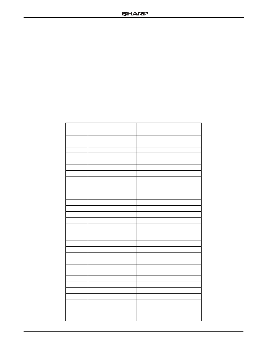
System-on-Chip
LH75400/01/10/11
Preliminary Data Sheet
6/4/03
53
Vectored Interrupt Controller (VIC)
All internal and external interrupts are routed to the
VIC, where hardware determines the interrupt priority
(see Table 14). The VIC is also where the appropriate
signal to the processor (IRQ or FIQ) is generated. The
processor services the interrupt as either a vectored
interrupt or a default-vectored interrupt.
The VIC accepts inputs from 32 interrupt source lines:
∑ Seven external
∑ Twenty-three internal
∑ Two used as software interrupts.
All 32 interrupt source lines can be enabled, disabled,
and cleared individually, and individual status can be
determined. On reset, all interrupts are disabled.
The VIC also accepts software-generated interrupts.
Software-generated interrupts use the same enabling
control as hardware-generated interrupts.
The VIC provides 32 interrupts:
∑ 16 vectored interrupts
∑ 16 or more default-vectored interrupts.
Any of the 32 interrupt source lines can be assigned
to any of the 16 interrupt vectors. Any line not explicitly
assigned to an interrupt vector is processed as a
default-vectored interrupt. At reset, all 32 lines become
default-vectored interrupts.
Each interrupt line can be explicitly identified as an
IRQ (default) or FIQ interrupt. Vectored-interrupt
servicing is only available for IRQ interrupts.
Table 14. Interrupt Channels
POSITION
DESCRIPTION
SOURCE
0
WDT
Watchdog Timer
1
Not Used
Available as a software interrupt
2
ARM7 DBGCOMMRX
Sourced by the ARM7TDMI-S Core
3
ARM7 DBGCOMMTX
Sourced by the ARM7TDMI-S Core
4
Timer0 Combined
Timer0
5
Timer1 Combined
Timer1
6
Timer2 Combined
Timer2
7
External Interrupt 0
Sourced by the GPIO Block
8
External Interrupt 1
Sourced by the GPIO Block
9
External Interrupt 2
Sourced by the GPIO Block
10
External Interrupt 3
Sourced by the GPIO Block
11
External Interrupt 4
Sourced by the GPIO Block
12
External Interrupt 5
Sourced by the GPIO Block
13
External Interrupt 6
Sourced by the GPIO Block
14
Not Used
Available as a software interrupt
15
RTC_ALARM
Real Time Clock
16
ADC TSCIRQ (combined) Analog-to-Digital Converter
17
ADC BrownOutINTR
Brown Out Detector
18
ADC PenIRQ
Analog-to-Digital Converter
19
LCD
LCD Controller
20
SSPTXINTR
Synchronous Serial Port
21
SSPRXINTR
Synchronous Serial Port
22
SSPRORINTR
Synchronous Serial Port
23
SSPRXTOINTR
Synchronous Serial Port
24
SSPINTR
Synchronous Serial Port
25
UART1 UARTRXINTR
UART1
26
UART1 UARTTXINTR
UART1
27
UART1 UARTINTR
UART1
28
UART0 UARTINTR
UART0
29
UART2 Interrupt
UART2
30
DMA
DMA
31
CAN
CAN (LH75401/LH75400)
Reserved (LH75411/LH75410)
LH75400/01/10/11
System-on-Chip
54
6/4/03
Preliminary Data Sheet
Reset, Clock, and Power Controller (RCPC)
The RCPC lets users control System Reset, clocks,
power management, and external interrupt condition-
ing via the AMBA APB interface. This control includes:
∑ Enabling and disabling various clocks
∑ Managing power-down sequencing
∑ Selecting the sources for various clocks.
The RCPC provides for an orderly start-up until the
crystal oscillator stabilizes and the PLL acquires lock. If
users want to change the system clock frequency dur-
ing normal operation, the RCPC ensures a seamless
transition between the old and new frequencies.
RCPC FEATURES
∑ Manages five Power Modes for minimizing power
consumption: Active, Standby, Sleep, Stop1, and
Stop2
∑ Generates the system clock (HCLK) from either the
PLL clock or the PLL-bypassed (oscillator) clock,
divided by 2, 4, 6, 8, ... 30
∑ Generates three UART clocks from oscillator clock
∑ Generates the 1 Hz RTC clock
∑ Generates the SSP and LCD clocks from HCLK,
divided by 1, 2, 4, 8, 16, 32, or 64
∑ Provides a selectable external clock output
∑ Generates system and RTC Resets based on an
external reset, Watchdog Timer reset, or soft reset
∑ Configures seven HIGH/LOW-level or rising/falling
edge-trigger external interrupts and converts them to
HIGH-level trigger interrupt outputs required by the VIC
∑ Generates remap outputs used by the memory map
decoder
∑ Provides an identification register
∑ Supports external or watchdog reset status.
Operating Modes
The LH75400/01/10/11 microcontrollers support
three operating modes:
∑ Normal Mode
∑ PLL Bypass Mode, where the internal PLL is
bypassed and an external clock source is used
∑ EmbeddedICE Mode, where the JTAG port
accesses the TAP Controller in the core and the core
is placed in Debug Mode.
The state of the TEST1, TEST2, and nRESETIN sig-
nals determines the operating mode entered at Power-
on Reset (see Table 15).
NOTE: TEST1, TEST2, and nRESETIN are latched on the rising
edge of nPOR. The microcontroller stays in that operating
mode until power is removed or nPOR transitions from LOW
to HIGH.
General Purpose Input/Output (GPIO)
The LH75400/01/10/11 microcontrollers have 10
GPIO ports:
∑ Seven 8-bit ports
∑ Two 7-bit ports
∑ One 6-bit port.
The GPIO ports are designated A through J and pro-
vide 76 bits of programmable input/output (see Table
16). Pins of all ports, except Port J, can be configured
as inputs or outputs. Port J is input only. Upon System
Reset, all ports default to inputs.
Table 15. Device Operating Modes
OPERATING MODE
TEST2
TEST1
nRESETIN
Reserved
0
0
0
PLL Bypass
0
0
1
Reserved
0
1
x
Reserved
1
0
0
EmbeddedICE
1
0
1
Normal
1
1
x
Table 16. GPIO Ports
PORT
PROGRAMMABLE PINS
A
8 Input/Output Pins
B
6 Input/Output Pins
C
8 Input/Output Pins
D
7 Input/Output Pins
E
8 Input/Output Pins
F
7 Input/Output Pins
G
8 Input/Output Pins
H
8 Input/Output Pins
I
8 Input/Output Pins
J
8 Input Pins
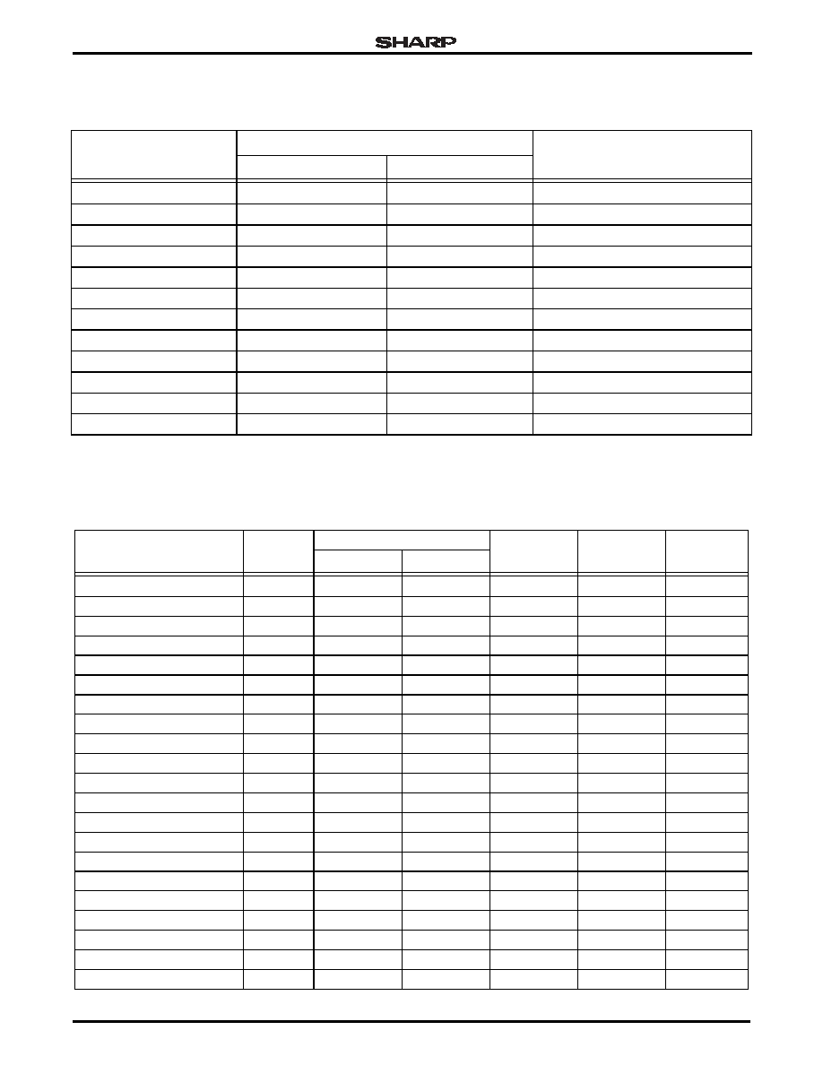
System-on-Chip
LH75400/01/10/11
Preliminary Data Sheet
6/4/03
55
Device Pin Multiplexing
NOTES:
1. MUSTN = Mono upper panel STN, dual and/or single panel.
2. MLSTN = Mono lower panel STN, dual panel only.
Table 17. LCD Panel Signal Multiplexing
EXTERNAL PIN
4-BIT STN (MONOCHROME)
8-BIT STN SINGLE PANEL
(MONOCHROME)
SINGLE PANEL
DUAL PANEL
LVCVD11
Reserved
MLSTN3
Reserved
LVCVD10
Reserved
MLSTN2
Reserved
LVCVD9
Reserved
MLSTN1
Reserved
LVCVD8
Reserved
MLSTN0
Reserved
LVCVD7
Reserved
Reserved
MUSTN7
LVCVD6
Reserved
Reserved
MUSTN6
LVCVD5
Reserved
Reserved
MUSTN5
LVCVD4
Reserved
Reserved
MUSTN4
LVCVD3
MUSTN3
MUSTN3
MUSTN3
LVCVD2
MUSTN2
MUSTN2
MUSTN2
LVCVD1
MUSTN1
MUSTN1
MUSTN1
LVCVD0
MUSTN0
MUSTN0
MUSTN0
Table 18. LCD External Pin Multiplexing (LH75401 and LH75411)
EXTERNAL PIN
DEFAULT
MODE
(NO LCD)
4-BIT MONO STN MODE
8-BIT
STN MODE
TFT
MODE
AD-TFT/
HR-TFT
MODE
SINGLE
DUAL
PG4/LCDVEEEN/LCDMOD
PG4
LCDVEEEN
LCDVEEEN
LCDVEEEN
LCDVEEEN
LCDMOD
PG3/LCDVDDEN
PG3
LCDVDDEN
LCDVDDEN
LCDVDDEN
LCDVDDEN
LCDVDDEN
PG2/LCDDSPLEN/LCDREV
PG2
LCDDSPLEN
LCDDSPLEN
LCDDSPLEN
LCDDSPLEN
LCDREV
PG1/LCDCLS
PG1
PG1
PG1
PG1
PG1
LCDCLS
PG0/LCDPS
PG0
PG0
PG0
PG0
PG0
LCDPS
PH7/LCDDCLK
PH7
LCDDCLK
LCDDCLK
LCDDCLK
LCDDCLK
LCDDCLK
PH6/LCDLP/LCDHRLP
PH6
LCDLP
LCDLP
LCDLP
LCDLP
LCDLP
PH5/LCDFP/LCDSPS
PH5
LCDFP
LCDFP
LCDFP
LCDFP
LCDFP
PH4/LCDEN/LCDEN
PH4
LCDEN
LCDEN
LCDEN
LCDEN
LCDEN
PH3/LCDVD11
PH3
PH3
MLSTN3
PH3
LCDVD11
LCDVD11
PH2/LCDVD10
PH2
PH2
MLSTN2
PH2
LCDVD10
LCDVD10
PH1/LCDVD9
PH1
PH1
MLSTN1
PH1
LCDVD9
LCDVD9
PH0/LCDVD8
PH0
PH0
MLSTN0
PH0
LCDVD8
LCDVD8
PI7/LCDVD7
PI7
PI7
PI7
STN7
LCDVD7
LCDVD7
PI6/LCDVD6
PI6
PI6
PI6
STN6
LCDVD6
LCDVD6
PI5/LCDVD5
PI5
PI5
PI5
STN5
LCDVD5
LCDVD5
PI4/LCDVD4
PI4
PI4
PI4
STN4
LCDVD4
LCDVD4
PI3/LCDVD3
PI3
MUSTN3
MUSTN3
STN3
LCDVD3
LCDVD3
PI2/LCDVD2
PI2
MUSTN2
MUSTN2
STN2
LCDVD2
LCDVD2
PI1/LCDVD1
PI1
MUSTN1
MUSTN1
STN1
LCDVD1
LCDVD1
PI0/LCDVD0
PI0
MUSTN0
MUSTN0
STN0
LCDVD0
LCDVD0

LH75400/01/10/11
System-on-Chip
56
6/4/03
Preliminary Data Sheet
Table 19. LCD External Pin Multiplexing (LH75400 and LH75410)
EXTERNAL PIN
DEFAULT
MODE (NO LCD)
4-BIT MONO STN MODE
8-BIT MONO
STN MODE
SINGLE
DUAL
PG4/LCDVEEEN
PG4
LCDVEEEN
LCDVEEEN
LCDVEEEN
PG3/LCDVDDEN
PG3
LCDVDDEN
LCDVDDEN
LCDVDDEN
PG2/LCDDSPLEN
PG2
LCDDSPLEN
LCDDSPLEN
LCDDSPLEN
PG1
PG1
PG1
PG1
PG1
PG0
PG0
PG0
PG0
PG0
PH7/LCDDCLK
PH7
LCDDCLK
LCDDCLK
LCDDCLK
PH6/LCDLP
PH6
LCDLP
LCDLP
LCDLP
PH5/LCDFP
PH5
LCDFP
LCDFP
LCDFP
PH4/LCDEN
PH4
LCDEN
LCDEN
LCDEN
PH3/LCDVD11
PH3
PH3
MLSTN3
PH3
PH2/LCDVD10
PH2
PH2
MLSTN2
PH2
PH1/LCDVD9
PH1
PH1
MLSTN1
PH1
PH0/LCDVD8
PH0
PH0
MLSTN0
PH0
PI7/LCDVD7
PI7
PI7
PI7
MUSTN7
PI6/LCDVD6
PI6
PI6
PI6
MUSTN6
PI5/LCDVD5
PI5
PI5
PI5
MUSTN5
PI4/LCDVD4
PI4
PI4
PI4
MUSTN4
PI3/LCDVD3
PI3
MUSTN3
MUSTN3
MUSTN3
PI2/LCDVD2
PI2
MUSTN2
MUSTN2
MUSTN2
PI1/LCDVD1
PI1
MUSTN1
MUSTN1
MUSTN1
PI0/LCDVD0
PI0
MUSTN0
MUSTN0
MUSTN0
System-on-Chip
LH75400/01/10/11
Preliminary Data Sheet
6/4/03
57
ELECTRICAL SPECIFICATIONS
NOTES:
1. Linear regulator disabled; use of the on-chip linear regulator provides optimal performance.
2. Linear regulator enabled.
3. Will operate to DC with PLL disabled
4. Processor is functional at minimum frequency, but not all peripherals may be enabled.
5. The maximum operating frequency is the crystal frequency ◊ 3.5.
Table 20. Absolute Maximum Ratings
PARAMETER
MINIMUM MAXIMUM
DC Core Supply Voltage (VDDC)
-0.3 V
2.4 V
DC I/O Supply Voltage (VDD)
-0.3 V
4.6 V
DC Analog Supply Voltage for ADC (VDDA0)
-0.3 V
4.6 V
DC Analog Supply Voltage for PLL (VDDA1)
-0.3 V
2.4 V
Storage Temperature (TSTG)
-55∞C
125∞C
Table 21. Recommended Operating Conditions
PARAMETER
MINIMUM
TYP.
MAXIMUM
NOTES
DC Core Supply Voltage (VDDC)
1.62 V
1.8 V
1.98 V
1
DC Analog Supply Voltage for ADC (VDDA0)
3.0 V
3.3 V
3.6 V
DC I/O Supply Voltage (VDD)
3.0 V
3.3 V
3.6 V
DC Analog Supply Voltage for PLL (VDDA1)
1.62 V
1.8 V
1.98 V
Clock Frequency (HCLK)
3.2667 MHz
64 MHz
1, 3, 4
Clock Period (tHCLK)
15.625 ns
306.1193 ns
1, 3, 4
Clock Frequency (HCLK)
4.375 MHz
70 MHz
2, 3, 4
Clock Period (tHCLK)
14.2857 ns
306.1193 ns
2, 3, 4
Crystal Frequency
14 MHz
20 MHz
5
Industrial Operating Temperature
-40∞C
25∞C
85∞C
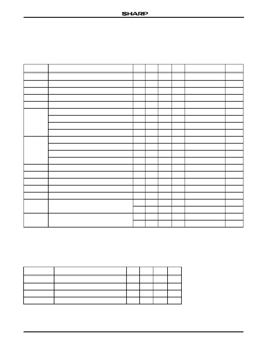
LH75400/01/10/11
System-on-Chip
58
6/4/03
Preliminary Data Sheet
DC Characteristics
All characteristics are specified over an operating
temperature of -40∞C to +85∞C, and at minimum and
maximum supply voltages.
NOTES:
1. VIL MAX. = 0.5 V for pin TCK with 50 pF load.
2. Running a Typical Application at 51.6 MHz.
3. Using external 1.8 V supply, internal regulator disabled.
4. Using Internal linear regulator.
Table 22. DC Characteristics
SYMBOL
PARAMETER
MIN. TYP. MAX. UNIT
CONDITIONS
NOTES
VIH
CMOS Input HIGH Voltage
2.0
V
VIL
CMOS Input LOW Voltage
0.8
V
1
VT+
Schmitt Trigger Positive Going Threshold
2.0
V
VT-
Schmitt Trigger Negative Going Threshold
0.8
V
Vhst
Schmitt Trigger Hysteresis
0.35
V
VOH
Output Drive 1
2.6
V
IOH = -2 mA
Output Drive 2
2.6
V
IOH = -4 mA
Output Drive 3
2.6
V
IOH = -6 mA
Output Drive 4
2.6
V
IOH = -8 mA
VOL
Output Drive 1
0.4
V
IOL = 2 mA
Output Drive 2
0.4
V
IOL = 4 mA
Output Drive 3
0.4
V
IOL = 6 mA
Output Drive 4
0.4
V
IOH = 8 mA
IIN
Input Leakage Current
-10
10
µ
A
VIN = VDD or GND
IACTIVE
Active Current
70
mA
2
ISTANDBY Standby Current
45
mA
2
ISLEEP
Sleep Current
4.0
mA
ISTOP1
Stop1 Current
3.0
mA
ISTOP2
Stop2 Current (RTC ON)
35
µ
A
3
120
µ
A
4
ISTOP2
Stop2 Current (RTC OFF)
23
µ
A
3
100
µ
A
4
Table 23. Linear Regulator DC Characteristics
SYMBOL
PARAMETER
MIN. TYP. MAX. UNIT
IQUIESCENT Quiescent Current
75
µ
A
ISLEEPLR
Current when Regulator is Disabled
8
µ
A
IOLR
Output Current Range
0.0
100
mA
VOLR
Output Voltage
1.84
V
System-on-Chip
LH75400/01/10/11
Preliminary Data Sheet
6/4/03
59
Analog-To-Digital Converter Electrical
Characteristics
Table 24 shows the derated specifications for
extended temperature operation. See Figure 10 for the
ADC transfer characteristics.
NOTES:
1. The analog section of the ADC takes 16 ◊ A2DCLK cycles per conversion,
plus 1 ◊ A2DCLK cycles to be made available in the PCLK domain.
An additional 3 ◊ PCLK cycles are required before being available on the APB.
2. The internal voltage reference is driven to nominal value VREF = 2.0 V.
Using the Reference Multiplexor, alternative low impedance (RS < 500) voltages
can be selected as reference voltages. The range of voltages allowed are specified above.
3. The analog input pins can be driven anywhere between the power supply rails.
If the voltage at the input to the ADC exceeds VREF+ or is below VREF-,
the A/D result will saturate appropriately at positive or negative full scale.
Trying to pull the analog input pins above or below the power supply rails will
cause protection diodes to be forward-biased, resulting in large current source/sink and
possible damage to the ADC.
4. Bandgap and other low-bandwidth circuitry operating. All other ADC blocks shut down.
Table 24. ADC Electrical Characteristics at Industrial Operating Range
PARAMETER
MIN.
TYP.
MAX.
UNITS
NOTES
A/D Resolution
10
10
Bits
Throughput Conversion
17
CLK Cycles
1
Acquisition Time
3
CLK Cycles
Clk Frequency
500
5,000
ns
Differential Non-Linearity
-0.99
4.5
LSB
Integral Non-Linearity
-3.5
+3.5
LSB
Offset Error
-35
+35
mV
Gain Error
-4.0
4.0
LSB
Reference Voltage Output
1.85
2.0
2.15
V
VREF-
VSSA
VSSA
VREF ±1.0 V
V
2
VREF+
VREF ±1.0 V
VREF
VDDA
V
2
Crosstalk between channels
-60
dB
Analog Input Voltage Range
0
VDDA
V
3
Analog Input Current
5
µ
A
Reference Input Current
5
µ
A
Analog input capacitance
15
pF
Operating Supply Voltage
3.0
3.6
V
Operating Current, VDDA
590
µ
A
Standby Current
180
µ
A
4
Stop Current, VDDA
< 1
µ
A
Brown Out Trip Point
2.63
V
Brown Out Hysterisis
120
mV
Operating Temperature
-40
85
∞C
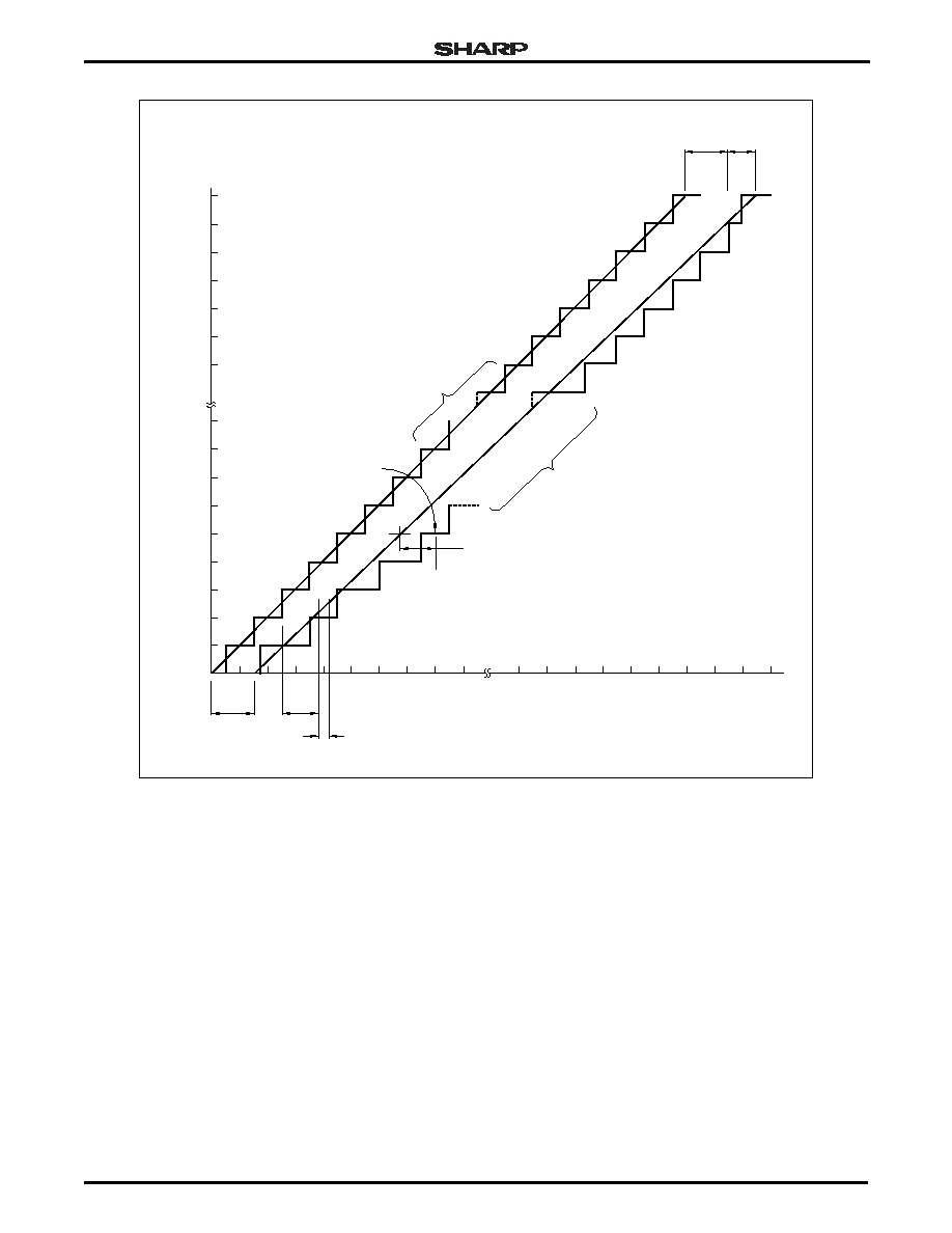
LH75400/01/10/11
System-on-Chip
60
6/4/03
Preliminary Data Sheet
Figure 10. ADC Transfer Characteristics
1015
1
2
3
4
5
6
7
8
9
1018
1019
1020
1021
1022
1023
1024
1016 1017 1018 1019
754xx-54
1020 1021 1022 1023 1024
1
2
3
4
5
6
7
8
9
INTEGRAL
NON-LINEARITY
ACTUAL
TRANSFER CURVE
IDEAL
TRANSFER CURVE
CENTER OF A
STEP OF THE ACTUAL
TRANSFER CURVE
OFFSET
ERROR
OFFSET
ERROR
LSB
DNL
GAIN
ERROR
System-on-Chip
LH75400/01/10/11
Preliminary Data Sheet
6/4/03
61
AC Characteristics
All signal transitions are measured from the 50%
point of the signal.
NOTE: The values in Table 25 represent the timing with no internal arbitration
delay and 1 wait state memory access. This is the worst case (fastest) timing.
Table 25. Memory Interface Signals
SIGNAL
I/O LOAD PARAMETER
MINIMUM
MAXIMUM
COMMENTS
D[15:0]
Out 50 pF
tOVD
tHCLK + 8 ns
Data output valid following address valid
D[15:0]
Out 50 pF
tOHD
3 ◊ tHCLK ≠ 6 ns
Data output invalid following address valid
D[15:0]
In
tIDD
2 tHCLK ≠ 18 ns Data input valid following address valid
nCS3 - nCS0
Out 30 pF
tOVCS
tHCLK + 6 ns
nCS output valid following address valid
nCS3 -nCS0
Out 30 pF
tOHCS
3 ◊ tHCLK ≠ 6 ns
nCS output invalid following address valid
nOE
Out 30 pF
tOVOE
tHCLK + 10 ns
nOE output valid following address valid
nOE
Out 30 pF
tOHOE
3 ◊ tHCLK ≠ 6 ns
nOE output invalid following address valid
nBLE1 - nBLE0 Out 30 pF
tOVBE
tHCLK + 10 ns
nBLE output valid following address valid
nBLE1 - nBLE0 Out 30 pF
tOHBER
3 ◊ tHCLK ≠ 6 ns
nBLE output invalid following address
valid, read cycle
nBLE1 - nBLE0 Out 30 pF
tOHBEW
2 ◊ tHCLK ≠ 6 ns
nBLE output invalid following address
valid, write cycle
nWE
Out 30 pF
tOVWE
tHCLK + 10 ns
nWE output valid following address valid
nWE
Out 30 pF
tOHWE
2 ◊ tHCLK ≠ 6 ns
nWE output invalid following address valid
nWAIT
In
tIVWAIT
2 tHCLK ≠ 18 ns nWAIT input valid following address valid
Table 26. Synchronous Serial Port
SIGNAL
I/O
LOAD
PARAMETER
MIN.
MAX.
COMMENT
SSPFRM
Out
50 pF
tOVSSPFRM
14 ns
SSPFRM output valid, referenced to SSPCLK
SSPTX
Out
50 pF
tOVSSPTX
12 ns
SSPTX output valid, referenced to SSPCLK
SSPRX
In
tISSPRX
22 ns
SSPRX input valid, referenced to SSPCLK
Table 27. Power-up Stabilization
PARAMETER
DESCRIPTION
MIN.
TYP.
MAX.
UNIT
tLREG
Linear regulator stabilization time after power-up
200
µ
s
tPLL
PLL stabilization time after power-up
8.57143
10
µ
s

LH75400/01/10/11
System-on-Chip
62
6/4/03
Preliminary Data Sheet
WAVEFORMS
Static Memory Controller Waveforms
Figure 12 shows the waveform and timing for an
External Static Memory Write, with one Wait State. Fig-
ure 13 shows the waveform and timing for an External
Static Memory Write, with two Wait States. Figure 14
shows the waveform and timing for an External Static
Memory Read, with one Wait State.
The SMC supports an nWAIT input that can be used
by an external device to extend the wait time during a
memory access. The SMC samples nWAIT at the
beginning of at the beginning of each system clock
cycle. The system clock cycle in which the nCSx signal
is asserted counts as the first wait state. See Figure 15.
The SMC recognizes that nWAIT is active within 2
clock cycles after it has been asserted. To assure that
the current access (read or write) will be extended by
nWAIT, program at least two wait states for this bank of
memory. If N wait states are programmed, the SMC
holds this state for N system clocks or until the SMC
detects that nWAIT is inactive, whichever occurs last.
As the number of wait states programmed increases,
the amount of delay before nWAIT must be asserted
also increases. If only 2 wait states are programmed,
nWAIT must be asserted in the clock cycle immediately
following the clock cycle during which the nCSx signal
is asserted. Once the SMC detects that the external
device has deactivated nWAIT, the SMC completes its
access in 3 system clock cycles.
The formula for the allowable delay between assert-
ing nCSx and asserting nWAIT is:
tASSERT = (system clock period) ◊ (Wait States - 1)
(where Wait States is from 2 to 31.)
Figure 11. Power-up Stabilization
LH754xx-100
VDD
LREG
tPLL
tLREG
VDDmin
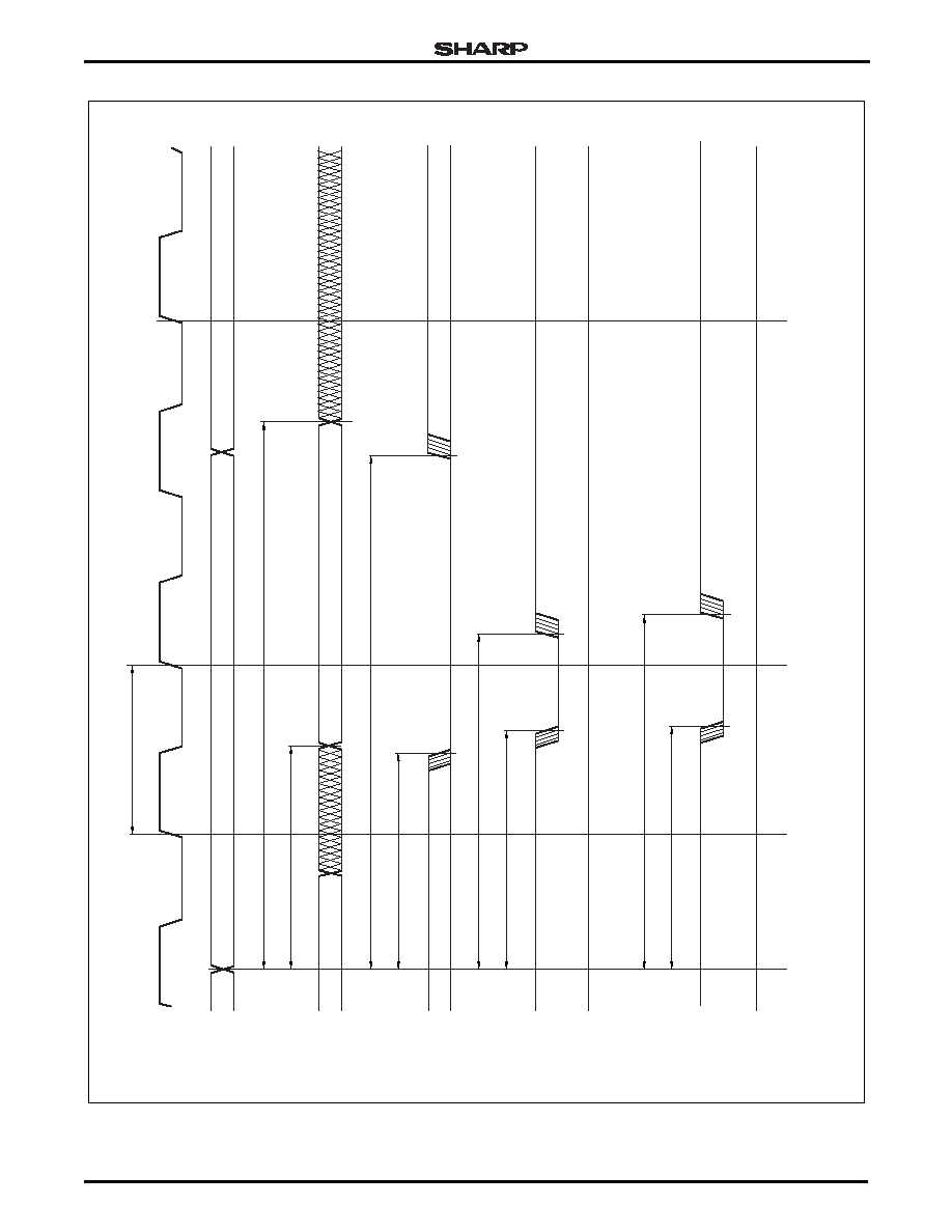
System-on-Chip
LH75400/01/10/11
Preliminary Data Sheet
6/4/03
63
Figure 12. External Static Memory Write, One Wait State
LH754xx-40
HCLK
A[23:0]
D[15:0]
nCSx
nWE
nW
AIT
nBLE[1:0]
nOE
tOHWE
tO
VWE
1 W
AIT
ST
A
T
E
tO
VD
tOHD
tO
VCS
tOHCS
D
ATA
ADDRESS
tOHBEW
tO
VBE
NO
TES:
1.
HCLK is an inter
nal signal, pro
vided f
or ref
erence only
.
2.
The corresponding b
yte lane enab
le(s) become activ
e
.
(See Note 1)
(See Note 2)
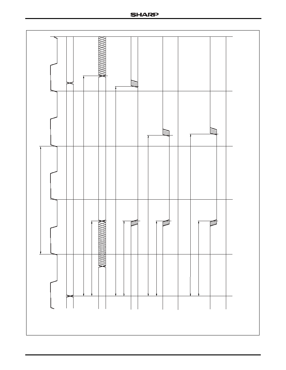
LH75400/01/10/11
System-on-Chip
64
6/4/03
Preliminary Data Sheet
Figure 13. External Static Memory Write, Two Wait States
HCLK
(See Note 1)
A[23:0]
D[15:0]
nCSx
nWE
nW
AIT
nBLE[1:0]
(See Note 2)
nOE
tOHWE
tO
VWE
2 W
AIT
ST
A
TES
tO
VD
tOHD
tO
VCS
tOHCS
D
ATA
ADDRESS
tOHBEW
tO
VBE
NO
TES:
1.
HCLK is an inter
nal signal, pro
vided f
or ref
erence only
.
2. The corresponding b
yte lane enab
le(s) become activ
e
.
LH754xx-42
System-on-Chip
LH75400/01/10/11
Preliminary Data Sheet
6/4/03
65
Figure 14. External Static Memory Read, One Wait State
1 W
AIT
ST
A
T
E
ADDRESS
D
ATA
tIDD
tO
VCS
tO
VBE
tO
V
O
E
tOHOE
tOHCS
tOHBER
HCLK
A[23:0]
D[15:0]
nCSx
nWE
nW
AIT
nOE
nBLE[1:0]
LH754xx-45
NO
TES:
1.
HCLK is an inter
nal signal, pro
vided f
or ref
erence only
.
2. The corresponding b
yte lane enab
le(s) become activ
e
.
(See Note 1)
(See Note 2)
LH75400/01/10/11
System-on-Chip
66
6/4/03
Preliminary Data Sheet
Figure 15. External Static Memory Read, nWAIT Active
HCLK
D[15:0]
A[23:0]
ADDRESS
D
ATA
nCSx
nOE
nWE
nW
AIT
nBLE[1:0]
LH754xx-47
NO
TES:
1.
HCLK is an inter
nal signal, pro
vided f
or ref
erence only
.
2. The corresponding b
yte lane enab
le(s) become activ
e
.
(See Note 1)
(See Note 2)
tIVW
AIT

System-on-Chip
LH75400/01/10/11
Preliminary Data Sheet
6/4/03
67
Synchronous Serial Port Waveform
Figure 16. Synchronous Serial Port Waveform
SSPCLK
SSPFRM
SSPTX
SSPRX
tO
VSSPFRM
tO
VSSPTX
tISSPRX
754xx-49
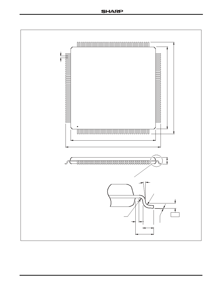
LH75400/01/10/11
System-on-Chip
68
6/4/03
Preliminary Data Sheet
PACKAGE SPECIFICATIONS
Figure 17.
144-pin LQFP
NOTE: Dimensions in mm.
22.00 NOM.
144LQFP-JEDEC
20.00 NOM.
22.00 NOM.
20.00 NOM.
0
∞
MIN.
0-7
∞
MIN.
1.00 REF.
0.60 ±0.15
0.20 MIN.
0.08 R. MIN.
0.08/0.20 R.
0.5 NOM.
1.40 MAX.
144LQFP (JEDEC MS-026)
TOP VIEW
0.25
GAUGE PLANE

System-on-Chip
LH75400/01/10/11
©2003 by SHARP Corporation
Reference Code SMA03009
SPECIFICATIONS ARE SUBJECT TO CHANGE WITHOUT NOTICE.
Suggested applications (if any) are for standard use; See Important Restrictions for limitations on special applications. See Limited
Warranty for SHARP's product warranty. The Limited Warranty is in lieu, and exclusive of, all other warranties, express or implied.
ALL EXPRESS AND IMPLIED WARRANTIES, INCLUDING THE WARRANTIES OF MERCHANTABILITY, FITNESS FOR USE AND
FITNESS FOR A PARTICULAR PURPOSE, ARE SPECIFICALLY EXCLUDED. In no event will SHARP be liable, or in any way responsible,
for any incidental or consequential economic or property damage.
NORTH AMERICA
EUROPE
JAPAN
SHARP Microelectronics of the Americas
5700 NW Pacific Rim Blvd.
Camas, WA 98607, U.S.A.
Phone: (1) 360-834-2500
Fax: (1) 360-834-8903
www.sharpsma.com
SHARP Microelectronics Europe
Division of Sharp Electronics (Europe) GmbH
Sonninstrasse 3
20097 Hamburg, Germany
Phone: (49) 40-2376-2286
Fax: (49) 40-2376-2232
www.sharpsme.com
SHARP Corporation
Electronic Components & Devices
22-22 Nagaike-cho, Abeno-Ku
Osaka 545-8522, Japan
Phone: (81) 6-6621-1221
Fax: (81) 6117-725300/6117-725301
www.sharp-world.com
TAIWAN
SINGAPORE
KOREA
SHARP Electronic Components
(Taiwan) Corporation
8F-A, No. 16, Sec. 4, Nanking E. Rd.
Taipei, Taiwan, Republic of China
Phone: (886) 2-2577-7341
Fax: (886) 2-2577-7326/2-2577-7328
SHARP Electronics (Singapore) PTE., Ltd.
438A, Alexandra Road, #05-01/02
Alexandra Technopark,
Singapore 119967
Phone: (65) 271-3566
Fax: (65) 271-3855
SHARP Electronic Components
(Korea) Corporation
RM 501 Geosung B/D, 541
Dohwa-dong, Mapo-ku
Seoul 121-701, Korea
Phone: (82) 2-711-5813 ~ 8
Fax: (82) 2-711-5819
CHINA
HONG KONG
SHARP Microelectronics of China
(Shanghai) Co., Ltd.
28 Xin Jin Qiao Road King Tower 16F
Pudong Shanghai, 201206 P.R. China
Phone: (86) 21-5854-7710/21-5834-6056
Fax: (86) 21-5854-4340/21-5834-6057
Head Office:
No. 360, Bashen Road,
Xin Development Bldg. 22
Waigaoqiao Free Trade Zone Shanghai
200131 P.R. China
Email: smc@china.global.sharp.co.jp
SHARP-ROXY (Hong Kong) Ltd.
3rd Business Division,
17/F, Admiralty Centre, Tower 1
18 Harcourt Road, Hong Kong
Phone: (852) 28229311
Fax: (852) 28660779
www.sharp.com.hk
Shenzhen Representative Office:
Room 13B1, Tower C,
Electronics Science & Technology Building
Shen Nan Zhong Road
Shenzhen, P.R. China
Phone: (86) 755-3273731
Fax: (86) 755-3273735