 | –≠–ª–µ–∫—Ç—Ä–æ–Ω–Ω—ã–π –∫–æ–º–ø–æ–Ω–µ–Ω—Ç: LH7A400-3 | –°–∫–∞—á–∞—Ç—å:  PDF PDF  ZIP ZIP |

Preliminary Data Sheet
8/27/03
1
LH7A400
Preliminary Data Sheet
32-Bit System-on-Chip
FEATURES
∑ ARM922TTM Core:
≠ 32-bit ARM9TDMITM RISC Core
≠ 16KB Cache: 8KB Instruction Cache and
8KB Data Cache
≠ MMU (Windows CE Enabled)
∑ High Performance (200 MHz)
∑ 80KB On-Chip Memory
∑ External Bus Interface
≠ 100 MHz
≠ Asynchronous SRAM/ROM/Flash
≠ Synchronous DRAM/Flash
≠ PCMCIA
≠ CompactFlash
∑ Clock and Power Management
≠ 32.768 kHz and 14.7456 MHz Oscillators
≠ Programmable PLL
∑ Low Power Modes
≠ Run (147 mA), Halt (41 mA), Standby (42
µ
A)
∑ Programmable LCD Controller
≠ Up to 1,024 ◊ 768 Resolution
≠ Supports STN, Color STN, HR-TFT, TFT
≠ Up to 64,000 Colors and 15 Gray Shades
∑ DMA (10 Channels)
≠ AC97
≠ MMC
≠ USB
∑ USB Client Interface (USB 1.1)
∑ Synchronous Serial Port (SSP)
≠ Motorola SPITM
≠ Texas Instruments SSI
≠ National MICROWIRETM
∑ Three Programmable Timers
∑ Three UARTs
≠ Classic IrDA (115 kbit/s)
∑ Smart Card Interface (ISO7816)
∑ DC-to-DC Converters
∑ MultiMediaCardTM Interface
∑ AC97 Codec Interface
∑ Smart Battery Monitor Interface
∑ Real Time Clock (RTC)
∑ Up to 60 General Purpose I/Os
∑ Programmable Interrupt Controller
∑ Watchdog Timer
∑ JTAG Debug Interface and Boundary Scan
∑ Operating Voltage
≠ 1.8 V Core
≠ 3.3 V Input/Output (1.8 V I/O Optional
1
)
∑ 5 V Tolerant Inputs (except oscillator pins
2
)
∑ Operating Temperature
≠ -40∞C to +85∞C
∑ 256-Ball PBGA or 256-Ball CABGA Package
DESCRIPTION
The LH7A400, powered by an ARM922T, is a com-
plete System-on-Chip with a high level of integration to
satisfy a wide range of requirements and expectations.
This high degree of integration lowers overall sys-
tem costs, reduces development cycle time and accel-
erates product introduction.
Motorola SPI is a trademark of Motorola, Inc.
National Semiconductor MICROWIRE is a trademark of
National Semiconductor Corporation.
Windows CE is a trademark of Microsoft Corporation.
NOTES:
1. Under development. Results pending further characterization.
2. Oscillator pins R13, T13, P15, and P16 are 1.8 V ±10%
LH7A400
32-Bit System-on-Chip
2
8/27/03
Preliminary Data Sheet
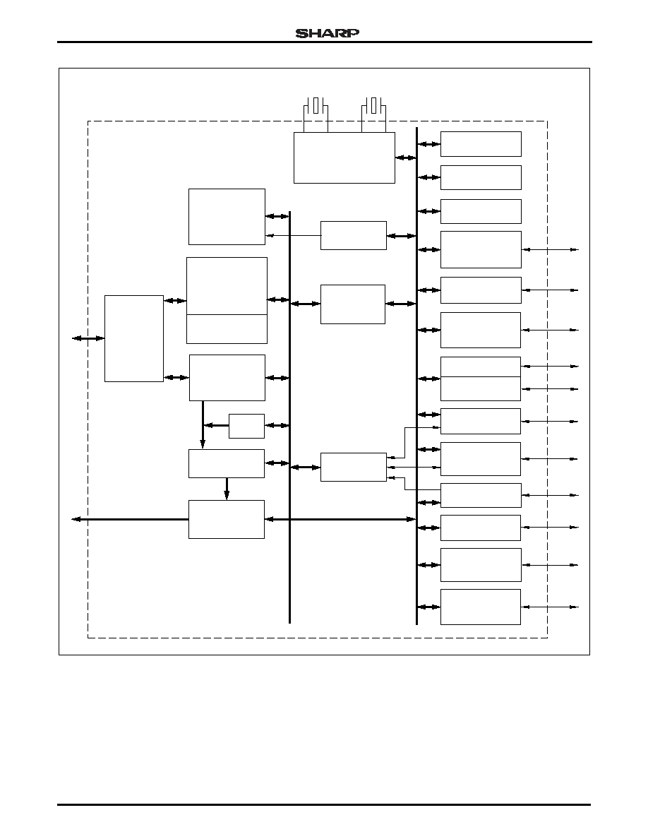
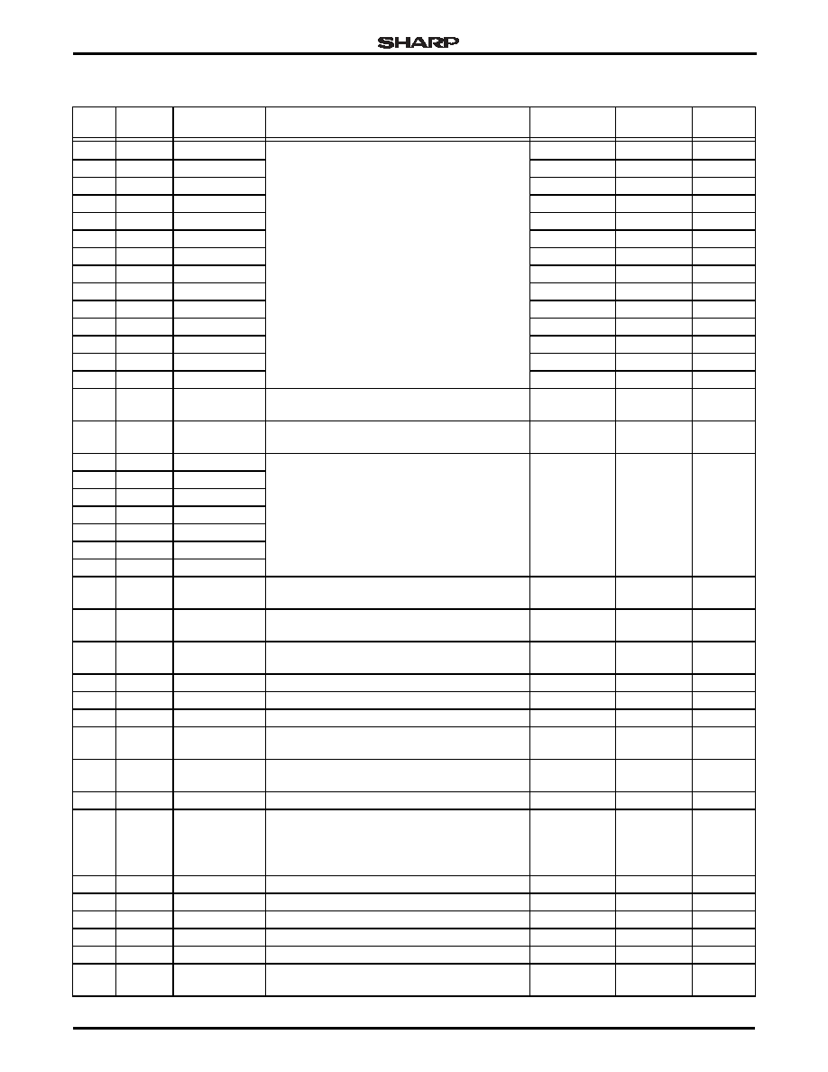
Figure 1. LH7A400 Block Diagram
LH7A400-1
OSCILLATOR,
PLL1 and PLL2, POWER
MANAGEMENT, and
RESET CONTROL
INTERRUPT
CONTROLLER
REAL TIME
CLOCK
14.7456 MHz
32.768 kHz
SYNCHRONOUS
DYNAMIC RAM
CONTROLLER
(SDMC)
PCMCIA/CF
CONTROLLER
COLOR LCD
CONTROLLER
80KB
SRAM
LCD AHB
BUS
STATIC
(ASYNCHRONOUS)
MEMORY
CONTROLLER
(SMC)
EXTERNAL
BUS
INTERFACE
ARM 922T
ADVANCED
PERIPHERAL
BUS BRIDGE
DMA
CONTROLLER
ADVANCED
HIGH-PERFORMANCE
BUS (AHB)
ADVANCED
PERPHERAL
BUS (APB)
AD-TFT
LCD TIMING
CONTROLLER
GENERAL
PURPOSE I/O
(60)
SYNCHRONOUS
SERIAL PORT
TIMER (3)
BATTERY
MONITOR
INTERFACE
USB DEVICE
INTERFACE
WATCHDOG
TIMER
IrDA
INTERFACE
UART (3)
MULTIMEDIACARD
INTERFACE
SMART CARD
INTERFACE
(ISO7816)
AUDIO CODEC
INTERFACE
ADVANCED AUDIO
CODEC (AC97)
DC to DC
INTERFACE
(2)
32-Bit System-on-Chip
LH7A400
Preliminary Data Sheet
8/27/03
3
Table 1. Functional Pin List
PBGA
PIN
CABGA
PIN
SIGNAL
DESCRIPTION
RESET
STATE
STANDBY
STATE
OUTPUT
DRIVE
G7
C10
VDD
I/O Ring Power
F1
F9
K7
F11
M1
F14
M5
G8
T6
H13
R14
J9
M14
K15
J11
L7
J12
N6
F13
N8
B14
N12
E10
N13
B8
P11
H7
B8
VSS
I/O Ring Ground
G3
C6
K4
D5
N5
D13
P6
E8
T14
F7
R16
G13
N16
H9
K13
J14
H9
K7
C15
L8
A11
L10
E8
L12
A5
M11
F7
M14
E1
C4
VDDC
Core Power
J4
D7
P3
D10
T8
F4
K9
F10
L13
J4
E15
J8
D12
K8
A7
L6
H5
G7
VSSC
Core Ground
M3
H4
L9
H8
T10
L4
N15
L9
H12
N3
B15
N7
C9
N10
G6
R5
LH7A400
32-Bit System-on-Chip
4
8/27/03
Preliminary Data Sheet
R11
P12
VDDA
Analog Power for PLL
N12
M10
P12
R13
VSSA
Analog Ground for PLL
T11
N11
D3
E4
nPOR
Power On Reset
Input
Input
H6
D1
nURESET
User Reset; should be pulled HIGH for normal or
JTAG operation.
Input
(Schmitt)
Input
D4
E2
WAKEUP
Wake Up
Input
(Schmitt)
Input
E4
F2
nPWRFL
Power Fail Signal
Input
(Schmitt)
Input
C2
D2
nEXTPWR
External Power
Input
(Schmitt)
Input
R13
R14
XTALIN
14.7456 MHz Crystal Oscillator pins. An external
clock source can be connected to XTALIN leav-
ing XTALOUT open.
Input
Input
T13
R15
XTALOUT
LOW
LOW
P16
N14
XTAL32IN
32.768 kHz Real Time Clock Crystal Oscillator
pins. An external clock source can be connected
to XTAL32IN leaving XTAL32OUT open.
Input
Input
P15
M13
XTAL32OUT
Output
Output
P14
M12
CLKEN
External Oscillator Clock Enable Output
LOW
LOW
8 mA
J6
J5
PGMCLK
Programmable Clock (14.7456 MHz MAX.)
LOW
LOW
8 mA
K11
P14
nCS0
Asynchronous Memory Chip Select 0
HIGH
HIGH
12 mA
K10
P16
nCS1
Asynchronous Memory Chip Select 1
HIGH
HIGH
12 mA
P13
N15
nCS2
Asynchronous Memory Chip Select 2
HIGH
HIGH
12 mA
M12
N16
nCS3/
nMMSPICS
∑ Asynchronous Memory Chip Select 3
∑ MultiMediaCard SPI Mode Chip Select
HIGH: nCS3
HIGH
12 mA
Table 1. Functional Pin List (Cont'd)
PBGA
PIN
CABGA
PIN
SIGNAL
DESCRIPTION
RESET
STATE
STANDBY
STATE
OUTPUT
DRIVE
32-Bit System-on-Chip
LH7A400
Preliminary Data Sheet
8/27/03
5
L12
L11
D0
Data Bus
LOW
LOW
12 mA
M15
L13
D1
N13
L14
D2
L16
K11
D3
L15
L16
D4
L14
K14
D5
H11
J15
D6
K12
J12
D7
J15
J10
D8
J13
H16
D9
J10
H14
D10
H15
H11
D11
H13
G16
D12
G15
G9
D13
G11
G14
D14
G12
G12
D15
F15
F15
D16
F12
E15
D17
E14
D16
D18
D16
F12
D19
H10
E13
D20
D14
D14
D21
F10
E12
D22
A16
B16
D23
A14
D12
D24
B13
A16
D25
C13
B13
D26
E12
B14
D27
G10
C12
D28
B12
A14
D29
B11
B12
D30
D11
A12
D31
M16
M15
A0/nWE1
∑ Asynchronous Address Bus
∑ Asynchronous Memory Write Byte Enable 1
HIGH: nWE1
HIGH
12 mA
N14
M16
A1/nWE2
∑ Asynchronous Address Bus
∑ Asynchronous Memory Write Byte Enable 2
HIGH: nWE2
HIGH
12 mA
Table 1. Functional Pin List (Cont'd)
PBGA
PIN
CABGA
PIN
SIGNAL
DESCRIPTION
RESET
STATE
STANDBY
STATE
OUTPUT
DRIVE
LH7A400
32-Bit System-on-Chip
6
8/27/03
Preliminary Data Sheet
M13
L15
A2/SA0
∑ Asynchronous Address Bus
∑ Synchronous Address Bus
LOW
LOW
12 mA
K16
K12
A3/SA1
LOW
LOW
12 mA
K15
K13
A4/SA2
LOW
LOW
12 mA
K14
K16
A5/SA3
LOW
LOW
12 mA
J8
J13
A6/SA4
LOW
LOW
12 mA
J16
J11
A7/SA5
LOW
LOW
12 mA
J14
J16
A8/SA6
LOW
LOW
12 mA
J9
H15
A9/SA7
LOW
LOW
12 mA
H16
H10
A10/SA8
LOW
LOW
12 mA
H14
H12
A11/SA9
LOW
LOW
12 mA
G16
G15
A12/SA10
LOW
LOW
12 mA
G14
G10
A13/SA11
LOW
LOW
12 mA
G13
G11
A14/SA12
LOW
LOW
12 mA
F16
F16
A15/SA13
LOW
LOW
12 mA
F14
E16
A16/SB0
∑ Asynchronous Address Bus
∑ Synchronous Device Bank Address 0
LOW
LOW
12 mA
E16
F13
A17/SB1
∑ Asynchronous Address Bus
∑ Synchronous Device Bank Address 1
LOW
LOW
12 mA
E13
E14
A18
Asynchronous Address Bus
LOW
LOW
12 mA
F11
D15
A19
D15
C16
A20
C16
C15
A21
B16
C14
A22
A15
B15
A23
A13
E11
A24
G8
D8
A25/SCIO
∑ Asynchronous Memory Address Bus
∑ Smart Card Interface I/O (Data)
LOW: A25
LOW
12 mA
F8
B7
A26/SCCLK
∑ Asynchronous Memory Address Bus
∑ Smart Card Interface Clock
LOW: A26
LOW
12 mA
A8
A7
A27/SCRST
∑ Asynchronous Memory Address Bus
∑ Smart Card Interface Reset
LOW: A27
LOW
12 mA
D8
C8
nOE
Asynchronous Memory Output Enable
HIGH
HIGH
12 mA
C8
F8
nWE0
Asynchronous Memory Write Byte Enable 0
HIGH
HIGH
12 mA
D10
D9
nWE3
Asynchronous Memory Write Byte Enable 3
HIGH
HIGH
8 mA
B10
E9
CS6/SCKE1_2
∑ Asynchronous Memory Chip Select 6
∑ Synchronous Memory Clock Enable 1 OR 2
LOW: CS6
LOW
12 mA
C10
A10
CS7/SCKE0
∑ Asynchronous Memory Chip Select 7
∑ Synchronous Memory Clock Enable 0
LOW: CS7
LOW
12 mA
G9
A11
SCKE3
Synchronous Memory Clock Enable 3
LOW
LOW
12 mA
A10
B10
SCLK
Synchronous Memory Clock
LOW
LOW
20 mA
(sink)
12 mA
(source)
C14
C13
nSCS0
Synchronous Memory Chip Select 0
HIGH
HIGH
12 mA
D13
A15
nSCS1
Synchronous Memory Chip Select 1
HIGH
HIGH
12 mA
E11
D11
nSCS2
Synchronous Memory Chip Select 2
HIGH
HIGH
12 mA
A12
E10
nSCS3
Synchronous Memory Chip Select 3
HIGH
HIGH
12 mA
C12
A13
nSWE
Synchronous Memory Write Enable
HIGH
HIGH
12 mA
C11
B11
nCAS
Synchronous Memory Column Address
Strobe Signal
HIGH
HIGH
12 mA
Table 1. Functional Pin List (Cont'd)
PBGA
PIN
CABGA
PIN
SIGNAL
DESCRIPTION
RESET
STATE
STANDBY
STATE
OUTPUT
DRIVE
32-Bit System-on-Chip
LH7A400
Preliminary Data Sheet
8/27/03
7
F9
C11
nRAS
Synchronous Memory Row Address Strobe Signal HIGH
HIGH
12 mA
A9
C9
DQM0
Synchronous Memory Data Mask 0
HIGH
HIGH
12 mA
B9
A9
DQM1
Synchronous Memory Data Mask 1
HIGH
HIGH
12 mA
D9
B9
DQM2
Synchronous Memory Data Mask 2
HIGH
HIGH
12 mA
E9
A8
DQM3
Synchronous Memory Data Mask 3
HIGH
HIGH
12 mA
J5
K1
PA0/LCDVD16
∑ GPIO Port A
∑ LCD Data bit 16. This CLCDC output signal is
always LOW.
Input: PA0
No Change
8 mA
K1
K2
PA1/LCDVD17
∑ GPIO Port A
∑ LCD Data bit 17. This CLCDC output signal is
always LOW.
Input: PA1
No Change
8 mA
K2
K3
PA2
GPIO Port A
Input
No Change
8 mA
K3
K4
PA3
K5
K6
PA4
L1
K5
PA5
L2
L1
PA6
L3
L2
PA7
L4
L3
PB0/UARTRX1
∑ GPIO Port B
∑ UART1 Receive Data Input
Input: PB0
No Change
8 mA
L5
M1
PB1/UARTTX3
∑ GPIO Port B
∑ UART3 Transmit Data Out
Input: PB1
LOW if
UART3 is
Enabled,
otherwise
No Change
8 mA
L7
M2
PB2/UARTRX3
∑ GPIO Port B
∑ UART3 Receive Data In
Input: PB2
No Change
8 mA
M2
M3
PB3/
UARTCTS3
∑ GPIO Port B
∑ UART3 Clear to Send
Input: PB3
No Change
8 mA
M4
L5
PB4/
UARTDCD3
∑ GPIO Port B
∑ UART3 Data Carrier Detect
Input: PB4
No Change
8 mA
N1
N1
PB5/
UARTDSR3
∑ GPIO Port B
∑ UART3 Data Set Ready
Input: PB5
No Change
8 mA
N2
N2
PB6/SWID/
SMBD
∑ GPIO Port B
∑ Single Wire Data
∑ Smart Battery Data
Input: PB6
Input if SMB
is Enabled,
otherwise
No Change
8 mA
N3
M4
PB7/SMBCLK
∑ GPIO Port B
∑ Smart Battery Clock
Input: PB7
Input if SMB
is Enabled,
otherwise
No Change
8 mA
P1
P1
PC0/UARTTX1
∑ GPIO Port C
∑ UART1 Transmit Data Output
LOW: PC0
No Change
12 mA
P2
P2
PC1/LCDPS
∑ GPIO Port C
∑ HR-TFT Power Save
LOW: PC1
No Change
12 mA
R1
R1
PC2/
LCDVDDEN
∑ GPIO Port C
∑ HR-TFT Power Sequence Control
LOW: PC2
No Change
12 mA
K6
M5
PC3/LCDREV
∑ GPIO Port C
∑ HR-TFT Gray Scale Voltage Reverse
LOW: PC3
No Change
12 mA
L8
P3
PC4/LCDSPS
∑ GPIO Port C
∑ HR-TFT Reset Row Driver Counter
LOW: PC4
No Change
12 mA
T1
N4
PC5/LCDCLS
∑ GPIO Port C
∑ HR-TFT Row Driver Clock
LOW: PC5
No Change
12 mA
Table 1. Functional Pin List (Cont'd)
PBGA
PIN
CABGA
PIN
SIGNAL
DESCRIPTION
RESET
STATE
STANDBY
STATE
OUTPUT
DRIVE

LH7A400
32-Bit System-on-Chip
8
8/27/03
Preliminary Data Sheet
T2
R2
PC6/LCDHRLP
∑ GPIO Port C
∑ LCD Latch Pulse
LOW: PC6
No Change
12 mA
R2
N5
PC7/LCDSPL
∑ GPIO Port C
∑ LCD Start Pulse Left
LOW: PC7
No Change
12 mA
M11
M9
PD0/LCDVD8
∑ GPIO Port D
∑ LCD Video Data Bus
LOW: PD0
LOW if
Dual-Panel
LCD is
Enabled;
otherwise,
No Change
12 mA
L11
K10
PD1/LCDVD9
LOW: PD1
K8
P10
PD2/LCDVD10
LOW: PD2
N11
T11
PD3/LCDVD11
LOW: PD3
R9
T12
PD4/LCDVD12
LOW: PD4
T9
R11
PD5/LCDVD13
LOW: PD5
P10
R12
PD6/LCDVD14
LOW: PD6
R10
T13
PD7/LCDVD15
LOW: PD7
L10
T9
PE0/LCDVD4
∑ GPIO Port E
∑ LCD Video Data Bus
Input: PE0
LOW if 8-bit
LCD is
Enabled,
otherwise
No Change
12 mA
N10
K9
PE1/LCDVD5
Input: PE1
M9
T10
PE2/LCDVD6
Input: PE2
M10
R10
PE3/LCDVD7
Input: PE3
A6
A5
PF0/INT0
∑ GPIO Port F
∑ External FIQ Interrupt. Interrupts can be level or
edge triggered and are internally debounced.
Input: PF0
(Schmitt)
No Change
8 mA
B6
B4
PF1/INT1
∑ GPIO Port F
∑ External IRQ Interrupts. Interrupts can be level
or edge triggered and are internally debounced.
Input: PF1
(Schmitt)
No Change
8 mA
C6
E7
PF2/INT2
Input: PF2
(Schmitt)
No Change
8 mA
H8
B3
PF3/INT3
∑ GPIO Port F
∑ External IRQ Interrupt. Interrupts can be level or
edge triggered and are internally debounced.
Input: PF3
(Schmitt)
No Change
8 mA
B5
C5
PF4/INT4/
SCVCCEN
∑ GPIO Port F
∑ External IRQ Interrupt. Interrupts can be level or
edge triggered and are internally debounced.
∑ Smart Card Supply Voltage Enable
Input: PF4
(Schmitt)
LOW if SCI
is Enabled;
otherwise,
No Change
8 mA
D6
D6
PF5/INT5/
SCDETECT
∑ GPIO Port F
∑ External IRQ Interrupt. Interrupts can be level or
edge triggered and are internally debounced.
∑ Smart Card Detection
Input: PF5
(Schmitt)
No Change
8 mA
E6
A4
PF6/INT6/
PCRDY1
∑ GPIO Port F
∑ External IRQ Interrupt. Interrupts can be level or
edge triggered and are internally debounced.
∑ Ready for Card 1 for PC Card (PCMCIA or
CompactFlash) in single or dual card mode
Input: PF6
(Schmitt)
No Change
8 mA
C5
A3
PF7/INT7/
PCRDY2
∑ GPIO Port F
∑ External IRQ Interrupt. Interrupts can be level or
edge triggered and are internally debounced.
∑ Ready for Card 2 for PC Card (PCMCIA or
CompactFlash) in single or dual card mode
Input: PF7
(Schmitt)
No Change
8 mA
R3
M6
PG0/nPCOE
∑ GPIO Port G
∑ Output Enable for PC Card (PCMCIA or
CompactFlash) in single or dual card mode
LOW: PG0
No Change
8 mA
T3
T1
PG1/nPCWE
∑ GPIO Port G
∑ Write Enable for PC Card (PCMCIA or
CompactFlash) in single or dual card mode
LOW: PG1
No Change
8 mA
Table 1. Functional Pin List (Cont'd)
PBGA
PIN
CABGA
PIN
SIGNAL
DESCRIPTION
RESET
STATE
STANDBY
STATE
OUTPUT
DRIVE

32-Bit System-on-Chip
LH7A400
Preliminary Data Sheet
8/27/03
9
L6
P4
PG2/nPCIOR
∑ GPIO Port G
∑ I/O Read Strobe for PC Card (PCMCIA or
CompactFlash) in single or dual card mode
LOW: PG2
No Change
8 mA
M6
R3
PG3/nPCIOW
∑ GPIO Port G
∑ I/O Write Strobe for PC Card (PCMCIA or
CompactFlash) in single or dual card mode
LOW: PG3
No Change
8 mA
N6
T2
PG4/nPCREG
∑ GPIO Port G
∑ Register Memory Access for PC Card (PCMCIA
or CompactFlash) in single or dual card mode
LOW: PG4
No Change
8 mA
M7
P5
PG5/nPCCE1
∑ GPIO Port G
∑ Card Enable 1 for PC Card (PCMCIA or
CompactFlash) in single or dual card mode.
This signal and nPCCE2 are used by the PC
Card for decoding low and high byte accesses.
LOW: PG5
No Change
8 mA
M8
R4
PG6/nPCCE2
∑ GPIO Port G
∑ Card Enable 2 for PC Card (PCMCIA or
CompactFlash) in single or dual card mode.
This signal and nPCCE1 are used by the PC
Card for decoding low and high byte accesses.
LOW: PG6
No Change
8 mA
N4
T3
PG7/PCDIR
∑ GPIO Port G
∑ Direction for PC Card (PCMCIA or
CompactFlash) in single or dual card mode
LOW: PG7
No Change
8 mA
P4
P6
PH0/
PCRESET1
∑ GPIO Port H
∑ Reset Card 1 for PC Card (PCMCIA or
CompactFlash) in single or dual card mode
Input: PH0
No Change
8 mA
R4
T4
PH1/CFA8/
PCRESET2
∑ GPIO Port H
∑ Address Bit 8 for PC Card (CompactFlash) in
single card mode
∑ Reset Card 2 for PC Card (PCMCIA or
CompactFlash) in dual card mode
Input: PH1
No Change
8 mA
T4
M7
PH2/
nPCSLOTE1
∑ GPIO Port H
∑ Enable Card 1 for PC Card (PCMCIA or
CompactFlash) in single or dual card mode.
This signal is used for gating other control sig-
nals to the appropriate PC Card.
Input: PH2
No Change
8 mA
N7
T5
PH3/CFA9/
PCMCIAA25/
nPCSLOTE2
∑ GPIO Port H
∑ Address Bit 9 for PC Card (CompactFlash) in
single card mode
∑ Address Bit 25 for PC Card (PCMCIA) in single
card mode
∑ Enable Card 2 for PC Card (PCMCIA or
CompactFlash) in dual card mode. This signal
is used for gating other control signals to the
appropriate PC Card.
Input: PH3
No Change
8 mA
P8
R6
PH4/
nPCWAIT1
∑ GPIO Port H
∑ WAIT Signal for Card 1 for PC Card (PCMCIA
or CompactFlash) in single or dual card mode
Input: PH4
No Change
8 mA
P5
R7
PH5/CFA10/
PCMCIAA24/
nPCWAIT2
∑ GPIO Port H
∑ Address Bit 10 for PC Card (CompactFlash) in
single card mode
∑ Address Bit 24 for PC Card (PCMCIA) in single
card mode
∑ WAIT Signal for Card 2 for PC Card (PCMCIA
or CompactFlash) in dual card mode
Input: PH5
No Change
8 mA
Table 1. Functional Pin List (Cont'd)
PBGA
PIN
CABGA
PIN
SIGNAL
DESCRIPTION
RESET
STATE
STANDBY
STATE
OUTPUT
DRIVE
LH7A400
32-Bit System-on-Chip
10
8/27/03
Preliminary Data Sheet
R5
P7
PH6/
AC97RESET
∑ GPIO Port H
∑ Audio Codec (AC97) Reset
Input: PH6
No Change
8 mA
T5
T6
PH7/nPC-
STATRE
∑ GPIO Port H
∑ Status Read Enable for PC Card (PCMCIA or
CompactFlash) in single or dual card mode
Input: PH7
No Change
8 mA
R6
T7
LCDFP
LCD Frame Synchronization pulse
LOW
LOW
12 mA
R8
R9
LCDLP
LCD Line Synchronization pulse
LOW
LOW
12 mA
P9
P9
LCDENAB/
LCDM
∑ LCD TFT Data Enable
∑ LCD STN AC Bias
LOW:
LCDENAB
LOW
12 mA
N9
N9
LCDDCLK
LCD Data Clock
LOW
LOW
12 mA
P7
M8
LCDVD0
LCD Video Data Bus
LOW
LOW
12 mA
R7
P8
LCDVD1
T7
R8
LCDVD2
N8
T8
LCDVD3
T15
T16
USBDP
USB Data Positive (Differential Pair)
Input
Input
75 mA
(nom.)
T16
R16
USBDN
USB Data Negative (Differential Pair)
Input
Input
75 mA
(nom.)
E7
C7
nPWME0
DC-DC Converter Pulse Width
Modulator 0 Enable
Input
Input
D7
A6
nPWME1
DC-DC Converter Pulse Width
Modulator 1 Enable
Input
Input
C7
B6
PWM0
DC-DC Converter Pulse Width
Modulator 0 Output during normal operation and
Polarity Selection input at reset
Input
Input
8 mA
B7
B5
PWM1
DC-DC Converter Pulse Width
Modulator 1 Output during normal operation and
Polarity Selection input at reset
Input
Input
8 mA
C4
A2
ACBITCLK
∑ Audio Codec (AC97) Clock
∑ Audio Codec (ACI) Clock
Input
Input
D5
A1
ACOUT
∑ Audio Codec (AC97) Output
∑ Audio Codec (ACI) Output
LOW
LOW
8 mA
B4
B2
ACSYNC
∑ Audio Codec (AC97) Synchronization
∑ Audio Codec (ACI) Synchronization
LOW
LOW
8 mA
A4
E6
ACIN
∑ Audio Codec (AC97) Input
∑ Audio Codec (ACI) Input
Input
Input
A3
C3
MMCCLK/
MMSPICLK
∑ MultiMediaCard Clock (20 MHz MAX.)
∑ MultiMediaCard SPI Mode Clock
LOW:
MMCCLK
LOW
8 mA
B3
B1
MMCCMD/
MMSPIDIN
∑ MultiMediaCard Command
∑ MultiMediaCard SPI Mode Data Input
Input:
MMCCMD
Input
8 mA
A2
D4
MMCDATA/
MMSPIDOUT
∑ MultiMediaCard Data
∑ MultiMediaCard SPI Mode Data Output
Input:
MMCDATA
Input
8 mA
E2
E1
UARTCTS2
UART2 Clear to Send Signal. This pin is an out-
put for JTAG boundary scan only.
Input
Input
E3
F3
UARTDCD2
UART2 Data Carrier Detect Signal. This pin is out-
put for JTAG boundary scan only.
Input
Input
E5
G4
UARTDSR2
UART2 Data Set Ready Signal
Input
Input
F2
G5
UARTIRTX1
IrDA Transmit
LOW
LOW
8 mA
F3
G6
UARTIRRX1
IrDA Receive. This pin is an output for JTAG
boundary scan only.
Input
Input
F4
F1
UARTTX2
UART2 Transmit Data Output
HIGH
HIGH
8 mA
Table 1. Functional Pin List (Cont'd)
PBGA
PIN
CABGA
PIN
SIGNAL
DESCRIPTION
RESET
STATE
STANDBY
STATE
OUTPUT
DRIVE
32-Bit System-on-Chip
LH7A400
Preliminary Data Sheet
8/27/03
11
NOTES: *Signals beginning with `n' are Active LOW.
J7
G3
UARTRX2
UART2 Receive Data Input. This pin is an output
for JTAG boundary scan only.
Input
Input
H4
J3
SSPCLK
Synchronous Serial Port Clock
LOW
LOW
8 mA
J1
J6
SSPRX
Synchronous Serial Port Receive
Input
Input
J2
J7
SSPTX
Synchronous Serial Port Transmit
LOW
LOW
8 mA
J3
J2
SSPFRM/
nSSPFRM
Synchronous Serial Port Frame Sync
Input:
nSSPFRM
Input
8 mA
F6
G2
COL0
Keyboard Interface
HIGH
HIGH
8 mA
F5
G1
COL1
G1
H3
COL2
G2
H5
COL3
G4
H6
COL4
G5
H7
COL5
H1
H2
COL6
H2
H1
COL7
H3
J1
TBUZ
Timer Buzzer (254 kHz MAX.)
LOW
LOW
8 mA
C3
F5
MEDCHG
Boot Device Media Change. Used with the
WIDTH0 and WIDTH1 pins to specify boot mem-
ory device.
Input
(Schmitt)
Input
P11
T14
WIDTH0
External Memory Width Pins. Also, used with
MEDCHG to specify the boot memory device size.
Input
(Schmitt)
Input
R12
T15
WIDTH1
D1
E3
BATOK
Battery OK
Input
(Schmitt)
Input
D2
F6
nBATCHG
Battery Change
Input
(Schmitt)
Input
A1
E5
TDI
JTAG Data In. This signal is internally pulled-up
to VDD.
Input with
Pull-up
Input with
Pull-up
B1
C2
TCK
JTAG Clock. This signal should be externally
pulled-up to VDD.
Input
Input
B2
D3
TDO
JTAG Data Out. This signal should be externally
pulled up to VDD with a 33 k
resistor.
Input
No Change
4 mA
C1
C1
TMS
JTAG Test Mode select. This signal is internally
pulled-up to VDD.
Input with
Pull-up
Input with
Pull-up
T12
P15
nTEST0
Test Pin 0. Internally pulled up to VDD. For Normal
mode, leave open. For JTAG mode, tie to GND.
See Table 2.
Input with
Pull-up
Input with
Pull-up
R15
P13
nTEST1
Test Pin 1. internally pulled up to VDD. For Normal
and JTAG mode, leave open. See Table 2.
Input with
Pull-up
Input with
Pull-up
Table 1. Functional Pin List (Cont'd)
PBGA
PIN
CABGA
PIN
SIGNAL
DESCRIPTION
RESET
STATE
STANDBY
STATE
OUTPUT
DRIVE
Table 2. nTest Pin Function
MODE
nTEST0
nTEST1
nURESET
JTAG
0
1
1
Normal
1
1
x

LH7A400
32-Bit System-on-Chip
12
8/27/03
Preliminary Data Sheet
NOTES:
1. The Intensity bit is identically generated for all three colors.
2. MU = Monochrome Upper
3. CU = Color Upper
4. CL = Color Lower
Table 3. LCD Data Multiplexing
PBGA
PIN
CABGA
PIN
LCD
DATA
SIGNAL
STN
TFT
AD-TFT/
HR-TFT
MONO 4-BIT
MONO 8-BIT
COLOR
SINGLE
PANEL
DUAL
PANEL
SINGLE
PANEL
DUAL
PANEL
SINGLE
PANEL
DUAL
PANEL
K1
K2
LCDVD17
LOW
J5
K1
LCDVD16
LOW
R10
T13
LCDVD15
MLSTN7
CLSTN7
Intensity
Intensity
P10
R12
LCDVD14
MLSTN6
CLSTN6
BLUE4
BLUE4
T9
R11
LCDVD13
MLSTN5
CLSTN5
BLUE3
BLUE3
R9
T12
LCDVD12
MLSTN4
CLSTN4
BLUE2
BLUE2
N11
T11
LCDVD11
MLSTN3
CLSTN3
BLUE1
BLUE1
K8
P10
LCDVD10
MLSTN2
CLSTN2
BLUE0
BLUE0
L11
K10
LCDVD9
MLSTN1
CLSTN1
GREEN4
GREEN4
M11
M9
LCDVD8
MLSTN0
CLSTN0
GREEN3
GREEN3
M10
R10
LCDVD7
MLSTN3
MUSTN7
MUSTN7
CUSTN7
CUSTN7
GREEN2
GREEN2
M9
T10
LCDVD6
MLSTN2
MUSTN6
MUSTN6
CUSTN6
CUSTN6
GREEN1
GREEN1
N10
K9
LCDVD5
MLSTN1
MUSTN5
MUSTN5
CUSTN5
CUSTN5
GREEN0
GREEN0
L10
T9
LCDVD4
MLSTN0
MUSTN4
MUSTN4
CUSTN4
CUSTN4
RED4
RED4
N8
T8
LCDVD3
MUSTN3
MUSTN3
MUSTN3
MUSTN3
CUSTN3
CUSTN3
RED3
RED3
T7
R8
LCDVD2
MUSTN2
MUSTN2
MUSTN2
MUSTN2
CUSTN2
CUSTN2
RED2
RED2
R7
P8
LCDVD1
MUSTN1
MUSTN1
MUSTN1
MUSTN1
CUSTN1
CUSTN1
RED1
RED1
P7
M8
LCDVD0
MUSTN0
MUSTN0
MUSTN0
MUSTN0
CUSTN0
CUSTN0
RED0
RED0
32-Bit System-on-Chip
LH7A400
Preliminary Data Sheet
8/27/03
13
Table 4. 256-Ball PBGA Package Numerical Pin List
BGA PIN
SIGNAL
RESET STATE
STANDBY STATE
A1
TDI
Input with Pull-up
Input with Pull-up
A2
MMCDATA/MMSPIDOUT
Input: MMSPIDOUT LOW
A3
MMCCLK/MMSPICLK
LOW: MMSPICLK
LOW
A4
ACIN
Input
Input
A5
VSS
A6
PF0/INT0
Input: PF0
No Change
A7
VDDC
A8
A27/SCRST
LOW: A27
LOW
A9
DQM0
HIGH
LOW
A10
SCLK
LOW
LOW
A11
VSS
A12
nSCS3
HIGH
HIGH
A13
A24
LOW
LOW
A14
D24
LOW
LOW
A15
A23
LOW
LOW
A16
D23
LOW
LOW
B1
TCK
Input
Input
B2
TDO
Input
No Change
B3
MMCCMD/MMSPIDIN
Input: MMSPIDIN
LOW
B4
ACSYNC
LOW
LOW
B5
PF4/INT4/SCVCCEN
Input: PF4
LOW if SCI is Enabled; otherwise, No Change
B6
PF1/INT1
Input: PF1
No Change
B7
PWM1
Input
Input
B8
VDD
B9
DQM1
HIGH
LOW
B10
CS6/SCKE1_2
LOW: CS6
LOW
B11
D30
LOW
LOW
B12
D29
LOW
LOW
B13
D25
LOW
LOW
B14
VDD
B15
VSSC
B16
A22
LOW
LOW
C1
TMS
Input with Pull-up
Input with Pull-up
C2
nEXTPWR
Input
Input
C3
MEDCHG
Input
Input
C4
ACBITCLK
Input
Input
C5
PF7/INT7/PCRDY2
Input: PF7
No Change
C6
PF2/INT2
PF2/INT2
No Change
C7
PWM0
Input
Input
C8
nWE0
HIGH
HIGH
C9
VSSC
C10
CS7/SCKE0
LOW: CS7
LOW
C11
nCAS
HIGH
HIGH
C12
nSWE
HIGH
HIGH
C13
D26
LOW
LOW

LH7A400
32-Bit System-on-Chip
14
8/27/03
Preliminary Data Sheet
C14
nSCS0
HIGH
HIGH
C15
VSS
C16
A21
LOW
LOW
D1
BATOK
Input
Input
D2
nBATCHG
Input
Input
D3
nPOR
Input
Input
D4
WAKEUP
Input
Input
D5
ACOUT
LOW
LOW
D6
PF5/INT5/SCDETECT
Input: PF5
No Change
D7
nPWME1
Input
Input
D8
nOE
HIGH
HIGH
D9
DQM2
HIGH
LOW
D10
nWE3
HIGH
HIGH
D11
D31
LOW
LOW
D12
VDDC
D13
nSCS1
HIGH
HIGH
D14
D21
LOW
LOW
D15
A20
LOW
LOW
D16
D19
LOW
LOW
E1
VDDC
E2
UARTCTS2
Input
Input
E3
UARTDCD2
Input
Input
E4
nPWRFL
Input
Input
E5
UARTDSR2
Input
Input
E6
PF6/INT6/PCRDY1
Input: PF6
No Change
E7
nPWME0
Input
Input
E8
VSS
E9
DQM3
HIGH
LOW
E10
VDD
E11
nSCS2
HIGH
HIGH
E12
D27
LOW
LOW
E13
A18
LOW
LOW
E14
D18
LOW
LOW
E15
VDDC
E16
A17/SB1
LOW: SBANK1
LOW
F1
VDD
F2
UARTIRTX1
LOW
LOW
F3
UARTIRRX1
Input
Input
F4
UARTTX2
HIGH
HIGH
F5
COL1
HIGH
HIGH
F6
COL0
HIGH
HIGH
F7
VSS
F8
A26/SCCLK
LOW: A26
LOW
F9
nRAS
HIGH
HIGH
F10
D22
LOW
LOW
Table 4. 256-Ball PBGA Package Numerical Pin List (Cont'd)
BGA PIN
SIGNAL
RESET STATE
STANDBY STATE

32-Bit System-on-Chip
LH7A400
Preliminary Data Sheet
8/27/03
15
F11
A19
LOW
LOW
F12
D17
LOW
LOW
F13
VDD
F14
A16/SB0
LOW: SBANK0
LOW
F15
D16
LOW
LOW
F16
A15/SA13
LOW: SA13
LOW
G1
COL2
HIGH
HIGH
G2
COL3
HIGH
HIGH
G3
VSS
G4
COL4
HIGH
HIGH
G5
COL5
HIGH
HIGH
G6
VSSC
G7
VDD
G8
A25/SCIO
LOW: A25
LOW
G9
SCKE3
LOW
LOW
G10
D28
LOW
LOW
G11
D14
LOW
LOW
G12
D15
LOW
LOW
G13
A14/SA12
LOW: SA12
LOW
G14
A13/SA11
LOW: SA11
LOW
G15
D13
LOW
LOW
G16
A12/SA10
LOW: SA10
LOW
H1
COL6
HIGH
HIGH
H2
COL7
HIGH
HIGH
H3
TBUZ
LOW
LOW
H4
SSPCLK
LOW
LOW
H5
VSSC
H6
nURESET
Input
Input
H7
VSS
H8
PF3/INT3
Input: PF3
No Change
H9
VSS
H10
D20
LOW
LOW
H11
D6
LOW
LOW
H12
VSSC
H13
D12
LOW
LOW
H14
A11/SA9
LOW: SA9
LOW
H15
D11
LOW
LOW
H16
A10/SA8
LOW: SA8
LOW
J1
SSPRX
Input
Input
J2
SSPTX
LOW
LOW
J3
SSPFRM/nSSPFRM
Input: nSSPFRM
Input
J4
VDDC
J5
PA0/LCDVD16
Input: PA0
No Change
J6
PGMCLK
LOW
LOW
J7
UARTRX2
Input
Input
Table 4. 256-Ball PBGA Package Numerical Pin List (Cont'd)
BGA PIN
SIGNAL
RESET STATE
STANDBY STATE
LH7A400
32-Bit System-on-Chip
16
8/27/03
Preliminary Data Sheet
J8
A6/SA4
LOW: SA4
LOW
J9
A9/SA7
LOW: SA7
LOW
J10
D10
LOW
LOW
J11
VDD
J12
VDD
J13
D9
LOW
LOW
J14
A8/SA6
LOW: SA6
LOW
J15
D8
LOW
LOW
J16
A7/SA5
LOW: SA5
LOW
K1
PA1/LCDVD17
Input: PA1
No Change
K2
PA2
Input
No Change
K3
PA3
Input
No Change
K4
VSS
K5
PA4
Input
No Change
K6
PC3/LCDREV
LOW: PC3
No Change
K7
VDD
K8
PD2/LCDVD10
LOW: PD2
LOW if Dual-Panel LCD is Enabled; otherwise,
No Change
K9
VDDC
K10
nCS1
HIGH
HIGH
K11
nCS0
HIGH
HIGH
K12
D7
LOW
LOW
K13
VSS
K14
A5/SA3
LOW: SA3
LOW
K15
A4/SA2
LOW: SA2
LOW
K16
A3/SA1
LOW: SA1
LOW
L1
PA5
Input
No Change
L2
PA6
Input
No Change
L3
PA7
Input
No Change
L4
PB0/UARTRX1
Input: PB0
No Change
L5
PB1/UARTTX3
Input: PB1
LOW if UART3 is Enabled, otherwise No Change
L6
PG2/nPCIOR
LOW: PG2
No Change
L7
PB2/UARTRX3
Input: PB2
No Change
L8
PC4/LCDSPS
LOW: PC4
No Change
L9
VSSC
L10
PE0/LCDVD4
Input: PE0
LOW if 8-bit LCD is Enabled, otherwise No Change
L11
PD1/LCDVD9
LOW: PD1
LOW if Dual-Panel LCD is Enabled; otherwise,
No Change
L12
D0
LOW
LOW
L13
VDDC
L14
D5
LOW
LOW
L15
D4
LOW
LOW
L16
D3
LOW
LOW
M1
VDD
M2
PB3/UARTCTS3
Input: PB3
No Change
M3
VSSC
Table 4. 256-Ball PBGA Package Numerical Pin List (Cont'd)
BGA PIN
SIGNAL
RESET STATE
STANDBY STATE
32-Bit System-on-Chip
LH7A400
Preliminary Data Sheet
8/27/03
17
M4
PB4/UARTDCD3
Input: PB4
No Change
M5
VDD
M6
PG3/nPCIOW
LOW: PG3
No Change
M7
PG5/nPCCE1
LOW: PG5
No Change
M8
PG6/nPCCE2
LOW: PG6
No Change
M9
PE2/LCDVD6
Input: PE2
LOW if 8-bit LCD is Enabled; otherwise No Change
M10
PE3/LCDVD7
Input: PE3
LOW if 8-bit LCD is Enabled; otherwise No Change
M11
PD0/LCDVD8
LOW: PD0
LOW if Dual-Panel LCD is Enabled; otherwise,
No Change
M12
nCS3/nMMSPICS
HIGH: nCS3
HIGH
M13
A2/SA0
LOW: SA0
LOW
M14
VDD
M15
D1
LOW
LOW
M16
A0/nWE1
HIGH: nWE1
HIGH
N1
PB5/UARTDSR3
Input: PB5
No Change
N2
PB6/SWID/SMBD
Input: PB6
Input if SMB is Enabled; otherwise No Change
N3
PB7/SMBCLK
Input: PB7
Input if SMB is Enabled; otherwise No Change
N4
PG7/PCDIR
LOW: PG7
No Change
N5
VSS
N6
PG4/nPCREG
LOW: PG4
No Change
N7
PH3/CFA9/PCMCIAA25/nPCSLOTE2 Input: PH3
No Change
N8
LCDVD3
LOW
LOW
N9
LCDDCLK
LOW
LOW
N10
PE1/LCDVD5
Input: PE1
LOW if 8-bit LCD is Enabled; otherwise No Change
N11
PD3/LCDVD11
LOW: PD3
LOW if Dual-Panel LCD is Enabled; otherwise,
No Change
N12
VDDA
N13
D2
LOW
LOW
N14
A1/nWE2
HIGH: nWE2
HIGH
N15
VSSC
N16
VSS
P1
PC0/UARTTX1
LOW: PC0
No Change
P2
PC1/LCDPS
LOW: PC1
No Change
P3
VDDC
P4
PH0/PCRESET1
Input: PH0
No Change
P5
PH5/CFA10/PCMCIAA24/nPCWAIT2
Input: PH5
No Change
P6
VSS
P7
LCDVD0
LOW
LOW
P8
PH4/nPCWAIT1
Input: PH4
No Change
P9
LCDENAB/LCDM
LOW: LCDENAB
LOW
P10
PD6/LCDVD14
LOW: PD6
LOW if Dual-Panel LCD is Enabled; otherwise,
No Change
P11
WIDTH0
Input
Input
P12
VSSA
P13
nCS2
HIGH
HIGH
P14
CLKEN
LOW
LOW
Table 4. 256-Ball PBGA Package Numerical Pin List (Cont'd)
BGA PIN
SIGNAL
RESET STATE
STANDBY STATE

LH7A400
32-Bit System-on-Chip
18
8/27/03
Preliminary Data Sheet
NOTE: `No Change' means the pin remains as it was programmed
prior to entering the Standby state.
P15
XTAL32OUT
Output
Output
P16
XTAL32IN
Input
Input
R1
PC2/LCDVDDEN
LOW: PC2
No Change
R2
PC7/LCDSPL
LOW: PC7
No Change
R3
PG0/nPCOE
LOW: PG0
No Change
R4
PH1/CFA8/PCRESET2
Input: PH1
No Change
R5
PH6/nAC97RESET
Input: PH6
No Change
R6
LCDFP
LOW
LOW
R7
LCDVD1
LOW
LOW
R8
LCDLP
LOW
LOW
R9
PD4/LCDVD12
LOW: PD4
LOW if Dual-Panel LCD is Enabled; otherwise,
No Change
R10
PD7/LCDVD15
LOW: PD7
LOW if Dual-Panel LCD is Enabled; otherwise,
No Change
R11
VDDA
R12
WIDTH1
Input
Input
R13
XTALIN
Input
Input
R14
VDD
R15
nTEST1
Input with Pull-up
Input with Pull-up
R16
VSS
T1
PC5/LCDCLS
LOW: PC5
No Change
T2
PC6/LCDHRLP
LOW: PC6
No Change
T3
PG1/nPCWE
LOW: PG1
No Change
T4
PH2/nPCSLOTE1
Input: PH2
No Change
T5
PH7/nPCSTATRE
Input: PH7
No Change
T6
VDD
T7
LCDVD2
LOW
LOW
T8
VDDC
T9
PD5/LCDVD13
LOW: PD5
LOW if Dual-Panel LCD is Enabled; otherwise,
No Change
T10
VSSC
T11
VSSA
T12
nTEST0
Input with Pull-up
Input with Pull-up
T13
XTALOUT
LOW
LOW
T14
VSS
T15
USBDP
HIGH
HIGH
T16
USBDN
LOW
LOW
Table 4. 256-Ball PBGA Package Numerical Pin List (Cont'd)
BGA PIN
SIGNAL
RESET STATE
STANDBY STATE

32-Bit System-on-Chip
LH7A400
Preliminary Data Sheet
8/27/03
19
Table 5. 256-Ball CABGA Package Numerical Pin List
CABGA PIN
SIGNAL
RESET STATE
STANDBY STATE
A1
ACOUT
LOW
LOW
A2
ACBITCLK
Input
Input
A3
PF7/INT7/PCRDY2
Input: PF7 (Schmitt) No Change
A4
PF6/INT6/PCRDY1
Input: PF6 (Schmitt) No Change
A5
PF0/INT0
Input: PF0 (Schmitt) No Change
A6
nPWME1
Input
Input
A7
A27/SCRST
LOW: A27
LOW
A8
DQM3
HIGH
HIGH
A9
DQM1
HIGH
HIGH
A10
CS7/SCKE0
LOW: CS7
LOW
A11
SCKE3
LOW
LOW
A12
D31
LOW
LOW
A13
nSWE
HIGH
HIGH
A14
D29
LOW
LOW
A15
nSCS1
HIGH
HIGH
A16
D25
LOW
LOW
B1
MMCCMD/MMSPIDIN
Input: MMCCMD
Input
B2
ACSYNC
LOW
LOW
B3
PF3/INT3
Input: PF3 (Schmitt) No Change
B4
PF1/INT1
Input: PF1 (Schmitt) No Change
B5
PWM1
Input
Input
B6
PWM0
Input
Input
B7
A26/SCCLK
LOW: A26
LOW
B8
VSS
B9
DQM2
HIGH
HIGH
B10
SCLK
LOW
LOW
B11
nCAS
HIGH
HIGH
B12
D30
LOW
LOW
B13
D26
LOW
LOW
B14
D27
LOW
LOW
B15
A23
LOW
LOW
B16
D23
LOW
LOW
C1
TMS
Input with Pull-up
Input with Pull-up
C2
TCK
Input
Input
C3
MMCCLK/MMSPICLK
LOW: MMCCLK
LOW
C4
VDDC
C5
PF4/INT4/SCVCCEN
Input: PF4 (Schmitt) LOW if SCI is Enabled; otherwise, No Change
C6
VSS
C7
nPWME0
Input
Input
C8
nOE
HIGH
HIGH
C9
DQM0
HIGH
HIGH
C10
VDD
C11
nRAS
HIGH
HIGH
LH7A400
32-Bit System-on-Chip
20
8/27/03
Preliminary Data Sheet
C12
D28
LOW
LOW
C13
nSCS0
HIGH
HIGH
C14
A22
LOW
LOW
C15
A21
LOW
LOW
C16
A20
LOW
LOW
D1
nURESET
Input (Schmitt)
Input
D2
nEXTPWR
Input (Schmitt)
Input
D3
TDO
Input
No Change
D4
MMCDATA/MMSPIDOUT
Input: MMCDATA
Input
D5
VSS
D6
PF5/INT5/SCDETECT
Input: PF5 (Schmitt) No Change
D7
VDDC
D8
A25/SCIO
LOW: A25
LOW
D9
nWE3
HIGH
HIGH
D10
VDDC
D11
nSCS2
HIGH
HIGH
D12
D24
LOW
LOW
D13
VSS
D14
D21
LOW
LOW
D15
A19
LOW
LOW
D16
D18
LOW
LOW
E1
UARTCTS2
Input
Input
E2
WAKEUP
Input (Schmitt)
Input
E3
BATOK
Input (Schmitt)
Input
E4
nPOR
Input
Input
E5
TDI
Input with Pull-up
Input with Pull-up
E6
ACIN
Input
Input
E7
PF2/INT2
Input: PF2 (Schmitt) No Change
E8
VSS
E9
CS6/SCKE1_2
LOW: CS6
LOW
E10
nSCS3
HIGH
HIGH
E11
A24
LOW
LOW
E12
D22
LOW
LOW
E13
D20
LOW
LOW
E14
A18
LOW
LOW
E15
D17
LOW
LOW
E16
A16/SB0
LOW
LOW
F1
UARTTX2
HIGH
HIGH
F2
nPWRFL
Input (Schmitt)
Input
F3
UARTDCD2
Input
Input
F4
VDDC
F5
MEDCHG
Input (Schmitt)
Input
F6
nBATCHG
Input (Schmitt)
Input
Table 5. 256-Ball CABGA Package Numerical Pin List
CABGA PIN
SIGNAL
RESET STATE
STANDBY STATE

32-Bit System-on-Chip
LH7A400
Preliminary Data Sheet
8/27/03
21
F7
VSS
F8
nWE0
HIGH
HIGH
F9
VDD
F10
VDDC
F11
VDD
F12
D19
LOW
LOW
F13
A17/SB1
LOW
LOW
F14
VDD
F15
D16
LOW
LOW
F16
A15/SA13
LOW
LOW
G1
COL1
HIGH
HIGH
G2
COL0
HIGH
HIGH
G3
UARTRX2
Input
Input
E5
UARTDSR2
Input
Input
G5
UARTIRTX1
LOW
LOW
G6
UARTIRRX1
Input
Input
G7
VSSC
G8
VDD
G9
D13
LOW
LOW
G10
A13/SA11
LOW
LOW
G11
A14/SA12
LOW
LOW
G12
D15
LOW
LOW
G13
VSS
G14
D14
LOW
LOW
G15
A12/SA10
LOW
LOW
G16
D12
LOW
LOW
H1
COL7
HIGH
HIGH
H2
COL6
HIGH
HIGH
H3
COL2
HIGH
HIGH
H4
VSSC
H5
COL3
HIGH
HIGH
H6
COL4
HIGH
HIGH
H7
COL5
HIGH
HIGH
H8
VSSC
H9
VSS
H10
A10/SA8
LOW
LOW
H11
D11
LOW
LOW
H12
A11/SA9
LOW
LOW
H13
VDD
H14
D10
LOW
LOW
H15
A9/SA7
LOW
LOW
H16
D9
LOW
LOW
J1
TBUZ
LOW
LOW
Table 5. 256-Ball CABGA Package Numerical Pin List
CABGA PIN
SIGNAL
RESET STATE
STANDBY STATE

LH7A400
32-Bit System-on-Chip
22
8/27/03
Preliminary Data Sheet
J2
SSPFRM/nSSPFRM
Input: nSSPFRM
Input
J3
SSPCLK
LOW
LOW
J4
VDDC
J5
PGMCLK
LOW
LOW
J6
SSPRX
Input
Input
J7
SSPTX
LOW
LOW
J8
VDDC
J9
VDD
J10
D8
LOW
LOW
J11
A7/SA5
LOW
LOW
J12
D7
LOW
LOW
J13
A6/SA4
LOW
LOW
J14
VSS
J15
D6
LOW
LOW
J16
A8/SA6
LOW
LOW
K1
PA0/LCDVD16
Input: PA0
No Change
K2
PA1/LCDVD17
Input: PA1
No Change
K3
PA2
Input
No Change
K4
PA3
Input
No Change
K5
PA5
Input
No Change
K6
PA4
Input
No Change
K7
VSS
K8
VDDC
K9
PE1/LCDVD5
Input: PE1
K10
PD1/LCDVD9
LOW: PD1
K11
D3
LOW
LOW
K12
A3/SA1
LOW
LOW
K13
A4/SA2
LOW
LOW
K14
D5
LOW
LOW
K15
VDD
K16
A5/SA3
LOW
LOW
L1
PA6
Input
No Change
L2
PA7
Input
No Change
L3
PB0/UARTRX1
Input: PB0
No Change
L4
VSSC
L5
PB4/UARTDCD3
Input: PB4
No Change
L6
VDDC
L7
VDD
L8
VSS
L9
VSSC
L10
VSS
L11
D0
LOW
LOW
L12
VSS
Table 5. 256-Ball CABGA Package Numerical Pin List
CABGA PIN
SIGNAL
RESET STATE
STANDBY STATE

32-Bit System-on-Chip
LH7A400
Preliminary Data Sheet
8/27/03
23
L13
D1
LOW
LOW
L14
D2
LOW
LOW
L15
A2/SA0
LOW
LOW
L16
D4
LOW
LOW
M1
PB1/UARTTX3
Input: PB1
LOW if UART3 is Enabled, otherwise No Change
M2
PB2/UARTRX3
Input: PB2
No Change
M3
PB3/UARTCTS3
Input: PB3
No Change
M4
PB7/SMBCLK
Input: PB7
Input if SMB is Enabled, otherwise No Change
M5
PC3/LCDREV
LOW: PC3
No Change
M6
PG0/nPCOE
LOW: PG0
No Change
M7
PH2/nPCSLOTE1
Input: PH2
No Change
M8
LCDVD0
LOW
LOW
M9
PD0/LCDVD8
LOW: PD0
LOW if Dual-Panel LCD is Enabled; otherwise,
No Change
M10
VDDA
M11
VSS
M12
CLKEN
LOW
LOW
M13
XTAL32OUT
Output
Output
M14
VSS
M15
A0/nWE1
HIGH: nWE1
HIGH
M16
A1/nWE2
HIGH: nWE2
HIGH
N1
PB5/UARTDSR3
Input: PB5
No Change
N2
PB6/SWID/SMBD
Input: PB6
Input if SMB is Enabled, otherwise No Change
N3
VSSC
N4
PC5/LCDCLS
LOW: PC5
No Change
N5
PC7/LCDSPL
LOW: PC7
No Change
N6
VDD
N7
VSSC
N8
VDD
N9
LCDDCLK
LOW
LOW
N10
VSSC
N11
VSSA
N12
VDD
N13
VDD
N14
XTAL32IN
Input
Input
N15
nCS2
HIGH
HIGH
N16
nCS3/nMMSPICS
HIGH: nCS3
HIGH
P1
PC0/UARTTX1
LOW: PC0
No Change
P2
PC1/LCDPS
LOW: PC1
No Change
P3
PC4/LCDSPS
LOW: PC4
No Change
P4
PG2/nPCIOR
LOW: PG2
No Change
P5
PG5/nPCCE1
LOW: PG5
No Change
P6
PH0/PCRESET1
Input: PH0
No Change
Table 5. 256-Ball CABGA Package Numerical Pin List
CABGA PIN
SIGNAL
RESET STATE
STANDBY STATE

LH7A400
32-Bit System-on-Chip
24
8/27/03
Preliminary Data Sheet
P7
PH6/AC97RESET
Input: PH6
No Change
P8
LCDVD1
LOW
LOW
P9
LCDENAB/LCDM
LOW: LCDENAB
LOW
P10
PD2/LCDVD10
LOW: PD2
No Change
P11
VDD
No Change
P12
VDDA
P13
nTEST1
Input with Pull-up
Input with Pull-up
P14
nCS0
HIGH
HIGH
P15
nTEST0
Input with Pull-up
Input with Pull-up
P16
nCS1
HIGH
HIGH
R1
PC2/LCDVDDEN
LOW: PC2
No Change
R2
PC6/LCDHRLP
LOW: PC6
No Change
R3
PG3/nPCIOW
LOW: PG3
No Change
R4
PG6/nPCCE2
LOW: PG6
No Change
R5
VSSC
R6
PH4/nPCWAIT1
Input: PH4
No Change
R7
PH5/CFA10/PCMCIAA24/nPCWAIT2
Input: PH5
No Change
R8
LCDVD2
LOW
LOW
R9
LCDLP
LOW
LOW
R10
PE3/LCDVD7
Input: PE3
No Change
R11
PD5/LCDVD13
LOW: PD5
No Change
R12
PD6/LCDVD14
LOW: PD6
No Change
R13
VSSA
R14
XTALIN
Input
Input
R15
XTALOUT
LOW
LOW
R16
USBDN
Input
Input
T1
PG1/nPCWE
LOW: PG1
No Change
T2
PG4/nPCREG
LOW: PG4
No Change
T3
PG7/PCDIR
LOW: PG7
No Change
T4
PH1/CFA8/PCRESET2
Input: PH1
No Change
T5
PH3/CFA9/PCMCIAA25/nPCSLOTE2 Input: PH3
No Change
T6
PH7/nPCSTATRE
Input: PH7
No Change
T7
LCDFP
LOW
LOW
T8
LCDVD3
LOW
LOW
T9
PE0/LCDVD4
Input: PE0
LOW if 8-bit LCD is Enabled, otherwise
No Change
T10
PE2/LCDVD6
Input: PE2
No Change
T11
PD3/LCDVD11
LOW: PD3
No Change
T12
PD4/LCDVD12
LOW: PD4
No Change
T13
PD7/LCDVD15
LOW: PD7
No Change
T14
WIDTH0
Input (Schmitt)
Input
T15
WIDTH1
Input (Schmitt)
Input
T16
USBDP
Input
Input
Table 5. 256-Ball CABGA Package Numerical Pin List
CABGA PIN
SIGNAL
RESET STATE
STANDBY STATE
32-Bit System-on-Chip
LH7A400
Preliminary Data Sheet
8/27/03
25
SYSTEM DESCRIPTIONS
ARM922T Processor
T h e L H 7 A 4 0 0 m i c r o c o n t r o l l e r f e a t u r e s t h e
ARM922T cached core with an Advanced High Perfor-
mance Bus (AHB) interface. The processor is a mem-
ber of the ARM9T family of processors. For more
information, see the ARM document, `ARM922T Tech-
nical Reference Manual', available on ARM's website
at www.arm.com.
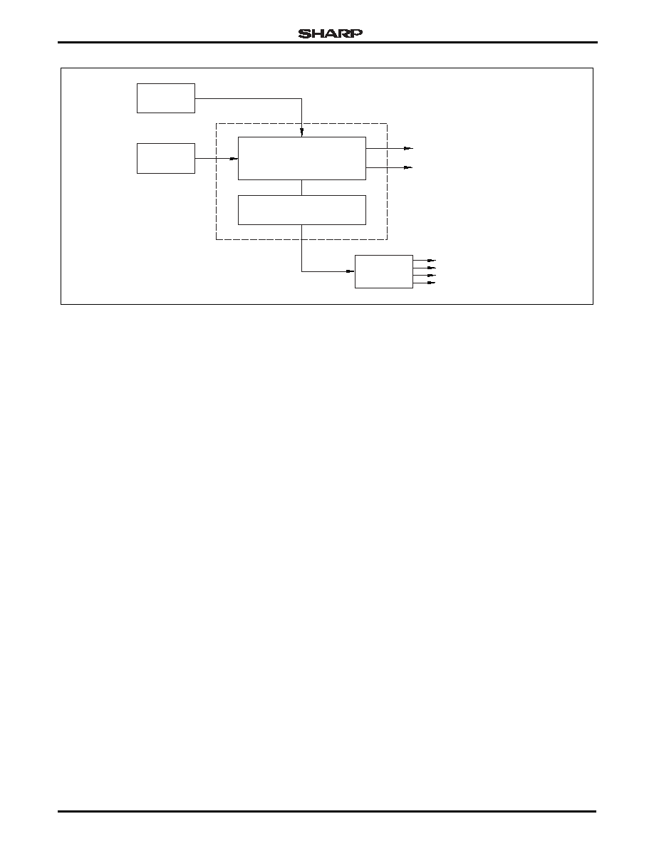
Clock and State Controller
The clocking scheme in the LH7A400 is based
around two primary oscillator inputs. These are the
14.7456 MHz input crystal and the 32.768 kHz real time
clock oscillator. See Figure 3. The 14.7456 MHz oscil-
lator is used to generate the main system clock
domains for the LH7A400, where as the 32.768 kHz is
used for controlling the power down operations and
real time clock peripheral. The clock and state control-
ler provides the clock gating and frequency division
necessary, and then supplies the clocks to the proces-
sor and to the rest of the system. The amount of clock
gating that actually takes place is dependent on the
current power saving mode selected.
The 32.768 kHz clock provides the source for the
Real Time Clock tree and power-down logic.This clock
is used for the power state control in the design and is
the only clock in the LH7A400 that runs permanently.
The 32.768 kHz clock is divided down to 1 Hz using a
ripple divider to save power. This generated 1 Hz clock
is used in the Real Time Clock counter.
The 14.7456 MHz source is used to generate the
main system clocks for the LH7A400. It is the source
for PLL1 and PLL2, it acts as the primary clock to the
peripherals and is the source clock to the Programma-
ble clock (PGM) divider.
PLL1 provides the main clock tree for the chip, it
generates the following clocks: FCLK, HCLK and
PCLK. FCLK is the clock that drives the ARM922T
core. HCLK is the main bus (AHB) clock, as such it
clocks all memory interfaces, bus arbitrators and the
AHB peripherals. HCLK is generated by dividing FCLK
by 1, 2, 3, or 4. HCLK can be gated by the system to
enable low power operation. PCLK is the peripheral
bus (APB) clock. It is generated by dividing HCLK by
either 2, 4, or 8.
PLL2 is used to generate a fixed frequency of
48 MHz for the USB peripheral.
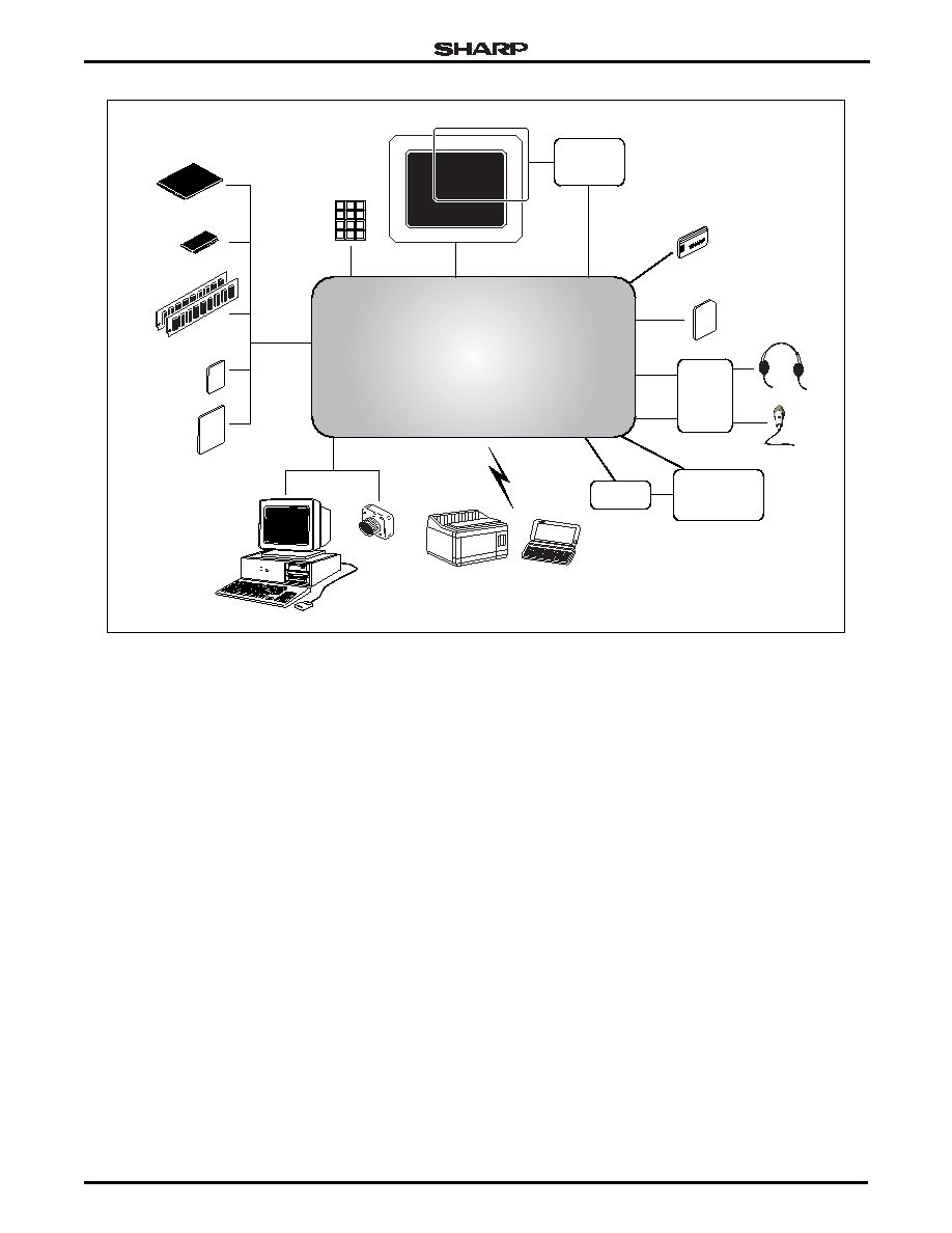
Figure 2. Application Diagram
CODEC
BATTERY
DC to DC
VOLTAGE
GENERATION
CIRCUITRY
MULTIMEDIA
CARD
TOUCH
SCREEN
CONTR.
MMC
SCI
PCMCIA
COMPACT
FLASH
UART
USB
SDRAM
SRAM
ROM
FLASH
DMA
AC97
STN/TFT/
AD-TFT
IR
GPIO
SSP
UART
LH7A400
PC
CARD
LH7A400-3
1
2
3
4
5
6
7
8
9
*
0
#
BMI
SMART
CARD
LH7A400
32-Bit System-on-Chip
26
8/27/03
Preliminary Data Sheet
Power Modes
The LH7A400 has three operational states: Run,
Halt, and Standby. In Run mode, all clocks are hard-
ware-enabled and the processor is clocked. Halt mode
stops the processor clock while waiting for an event
such as a key press, but the device continues to func-
tion. Finally, Standby equates to the computer being
switched `off', i.e. no display (LCD disabled) and the
main oscillator is shut down. The 32.768 kHz oscillator
operates in all three modes.
Reset Modes
There are three external signals that can generate
resets to the LH7A400; these are nPOR (power on
reset), nPWRFL (power failure) and nURESET (user
reset). If any of these are active, a system reset is gen-
erated internally. A nPOR reset performs a full system
reset. The nPWRFL and nURESET resets will perform
a full system reset except for the SDRAM refresh con-
trol, SDRAM Global Configuration, SDRAM Device
Configuration and the RTC peripheral registers. The
SDRAM controller will issue a self-refresh command to
external SDRAM before the system enters this reset
(the nPWRFL and nURESET resets only, not so for the
nPOR reset). This allows the system to maintain its
Real Time Clock and SDRAM contents. On coming out
of reset, the chip enters Standby mode. Once in Run
mode the PWRSR register can be interrogated to deter-
mine the nature of the reset, and the trigger source,
after which software can then take appropriate actions.
Data Paths
The data paths in the LH7A400 are:
∑ The AMBA AHB bus
∑ The AMBA APB bus
∑ The External Bus Interface
∑ The LCD AHB bus
∑ The DMA busses.
AMBA AHB BUS
The Advanced Microprocessor Bus Architecture
Advanced High-performance Bus (AMBA AHB) bus is a
high speed 32-bit-wide data bus. The AMBA AHB is for
high-performance, high clock frequency system modules.
Peripherals that have high bandwidth requirements
are connected to the LH7A400 core processor using
the AHB bus. These include the external and internal
memory interfaces, the LCD registers, palette RAM
and the bridge to the Advanced Peripheral Bus (APB)
interface. The APB Bridge transparently converts the
AHB access into the slower speed APB accesses. All
of the control registers for the APB peripherals are pro-
grammed using the AHB - APB bridge interface. The
main AHB data and address lines are configured using
a multiplexed bus. This removes the need for tri-state
buffers and bus holders, and simplifies bus arbitration.
Figure 3. Clock and State Controller Block Diagram
14.7456 MHz
MAIN OSC.
HCLK
32.768 kHz
RTC OSC.
/2, /4, /8
PCLKs
FCLK
HCLK
(TO PROCESSOR CORE)
LH7A400-4
STATE CONTROLLER
DIVIDE REGISTER

32-Bit System-on-Chip
LH7A400
Preliminary Data Sheet
8/27/03
27
AMBA APB BUS
The AMBA APB bus is a lower-speed 32-bit-wide
peripheral data bus. The speed of this bus is selectable
to be a divide-by-2, divide-by-4 or divide-by-8 of the
speed of the AHB bus.
EXTERNAL BUS INTERFACE
The External Bus Interface (EBI) provides a 32-bit
wide, high speed gateway to external memory devices.
The memory devices supported include:
∑ Asynchronous RAM/ROM/Flash
∑ Synchronous DRAM/Flash
∑ PCMCIA interfaces
∑ Compact Flash interfaces.
The EBI can be controlled by either the Asynchro-
nous memory controller or Synchronous memory con-
troller. There is an arbiter on the EBI input, with priority
given to the Synchronous Memory Controller interface.
LCD AHB BUS
The LCD controller has its own local memory bus
that connects it to the system's embedded memory and
external SDRAM. The function of this local data bus is
to allow the LCD controller to perform its video refresh
function without congesting the AHB bus. This leads to
better system performance and lower power consump-
tion. There is an arbiter on both the embedded memory
and the synchronous memory controller. In both cases
the LCD bus is given priority.
DMA BUSES
The LH7A400 has a DMA system that connects the
higher speed/higher data volume APB peripherals
(MMC, USB and AC97) to the AHB bus. This enables
the efficient transfer of data between these peripherals
and external memory without the intervention of the
ARM922T core. The DMA engine does not support
memory to memory transfers.
Memory Map
The LH7A400 system has a 32-bit-wide address bus.
This allows it to address up to 4GB of memory. This
memory space is subdivided into a number of memory
banks; see Figure 4. Four of these banks (each of
256MB) are allocated to the Synchronous memory con-
troller. Eight of the banks (again, each 256MB) are allo-
cated to the Asynchronous memory controller. Two of
these eight banks are designed for PCMCIA systems.
Part of the remaining memory space is allocated to the
embedded SRAM, and to the control registers of the
AHB and APB. The rest is unused.
The LH7A400 can boot from either synchronous or
asynchronous ROM/Flash. The selection is determined
by the value of the MEDCHG pin at Power On Reset as
shown in Table 6. When booting from synchronous
memory, then synchronous bank 4 (nSCS3) is mapped
into memory location zero. When booting from asyn-
chronous memory then asynchronous memory bank 0
(nSCS0) is mapped into memory location zero.
Figure 4 shows the memory map of the LH7A400
system for the two boot modes.
Once the LH7A400 has booted, the boot code can
configure the ARM922T MMU to remap the low mem-
ory space to a location in RAM. This allows the user to
set the interrupt vector table.
Interrupt Controller
The LH7A400 interrupt controller is designed to con-
trol the interrupts from 28 different sources. Four inter-
rupt sources are mapped to the FIQ input of the
ARM922T and 24 are mapped to the IRQ input. FIQs
have a higher priority than the IRQs. If two interrupts
with the same priority become active at the same time,
the priority must be resolved in software.
When an interrupt becomes active, the interrupt con-
troller generates a FIQ or IRQ if the corresponding
mask bit is set. No latching of interrupts takes place in
the controller. After a Power On Reset all mask register
bits are cleared, therefore masking all interrupts.
Hence, enabling of the mask register must be done by
software after a power-on-reset.
Table 6. Boot Modes
BOOT MODE
LATCHED
BOOT-
WIDTH1
LATCHED
BOOT-
WIDTH0
LATCHED
MEDCHG
8-bit ROM
0
0
0
16-bit ROM
0
1
0
32-bit ROM
1
0
0
32-bit ROM
1
1
0
16-bit SFlash
(Initializes Mode Register)
0 0 1
16-bit SROM
(Initializes Mode Register)
0 1 1
32-bit SFlash
(Initializes Mode Register)
1 0 1
32-bit SROM
(Initializes Mode Register)
1 1 1
LH7A400
32-Bit System-on-Chip
28
8/27/03
Preliminary Data Sheet
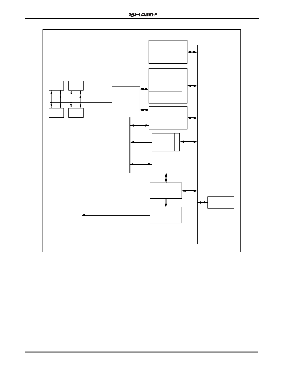
External Bus Interface
The external memory system allows the ARM922T,
LCD controller and DMA engine access to an external
memory system. The LCD controller has access to an
internal frame buffer in embedded SRAM and an exten-
sion buffer in Synchronous Memory for large displays.
The processor and DMA engine share the main system
bus, providing access to all external memory devices
and the embedded SRAM frame buffer.
An arbitration unit ensures that control over the
External Bus Interface (EBI) is only granted when an
existing access has been completed. See Figure 5.
Embedded SRAM
The amount of Embedded SRAM contained in the
LH7A400 is 80KB. This Embedded memory is designed
to be used for storing code, data, or LCD frame data
and to be contiguous with external SDRAM. The 80KB
is large enough to store a QVGA panel (320 ◊ 240) at 8
bits per pixel, equivalent to 70KB of information.
Containing the frame buffer on chip reduces the
overall power consumed in any application that uses
the LH7A400. Normally, the system has to perform
external accesses to acquire this data. The LCD con-
troller is designed to automatically use an overflow
frame buffer in SDRAM if a larger screen size is
required. This overflow buffer can be located on any
4KB page boundary in SDRAM, allowing software to
set the MMU (in the LCD controller) page tables such
that the two memory areas appear contiguous. Byte,
Half-Word and Word accesses are permissible.
Asynchronous Memory Controller
The Asynchronous memory controller is incorpo-
rated as part of the memory controller to provide an
interface between the AMBA AHB system bus and
external (off-chip) memory devices.
The Asynchronous Memory Controller provides sup-
port for up to eight independently configurable memory
banks simultaneously. Each memory bank is capable
of supporting:
∑ SRAM
∑ ROM
∑ Flash EPROM
∑ Burst ROM memory.
Each memory bank may use devices using either 8-,
16-, or 32-bit external memory data paths. The memory
controller can be configured to support either little-
endian or big-endian operation.
The memory banks can be configured to support:
∑ Non-burst read and write accesses only to high-
speed CMOS static RAM.
∑ Non-burst write accesses, nonburst read accesses
and asynchronous page mode read accesses to
fast-boot block flash memory.
Figure 4. Memory Mapping for Each Boot Mode
ASYNCHRONOUS MEMORY (nCS0)
F000.0000
SYNCHRONOUS MEMORY (nSCS2)
SYNCHRONOUS MEMORY (nSCS1)
D000.0000
SYNCHRONOUS MEMORY (nSCS0)
RESERVED
B001.4000
EMBEDDED SRAM
RESERVED
8000.3800
E000.0000
C000.0000
AHB INTERNAL REGISTERS
APB INTERNAL REGISTERS
8000.0000
ASYNCHRONOUS MEMORY (CS7)
ASYNCHRONOUS MEMORY (CS6)
6000.0000
PCMCIA/CompactFlash (nPCSLOTE2)
PCMCIA/CompactFlash (nPCSLOTE1)
4000.0000
ASYNCHRONOUS MEMORY (nCS3)
ASYNCHRONOUS MEMORY (nCS2)
2000.0000
7000.0000
5000.0000
B000.0000
8000.2000
3000.0000
1000.0000
ASYNCHRONOUS MEMORY (nCS1)
SYNCHRONOUS ROM (nSCS3)
0000.0000
SYNCHRONOUS MEMORY BOOT
SYNCHRONOUS MEMORY (nSCS3)
SYNCHRONOUS MEMORY (nSCS2)
SYNCHRONOUS MEMORY (nSCS1)
SYNCHRONOUS MEMORY (nSCS0)
RESERVED
EMBEDDED SRAM
RESERVED
AHB INTERNAL REGISTERS
APB INTERNAL REGISTERS
ASYNCHRONOUS MEMORY (CS7)
ASYNCHRONOUS MEMORY (CS6)
PCMCIA/CompactFlash (nPCSLOTE2)
PCMCIA/CompactFlash (nPCSLOTE1)
ASYNCHRONOUS MEMORY (nCS3)
ASYNCHRONOUS MEMORY (nCS2)
ASYNCHRONOUS MEMORY (nCS1)
ASYNCHRONOUS ROM (nCS0)
256MB
256MB
256MB
256MB
256MB
256MB
256MB
256MB
256MB
80KB
256MB
256MB
256MB
ASYNCHRONOUS MEMORY BOOT
LH7A400-6
32-Bit System-on-Chip
LH7A400
Preliminary Data Sheet
8/27/03
29
Figure 5. External Bus Interface Block Diagram
LH7A400-8
SYNCHRONOUS
DYNAMIC
MEMORY
CONTROLLER
(SDMC)
PCMCIA/CF
SUPPORT
ARBITER
COLOR LCD
CONTROLLER
(CLCDC)
80KB
EMBEDDED
SRAM
LCD
AHB
ASYNCHRONOUS
STATIC
MEMORY
CONTROLLER
(SMC)
EXTERNAL
BUS
INTERFACE
(EBI)
SDRAM
DATA
ADDRESS
and
CONTROL
SDRAM
ARM922T
LCD MEMORY
MANAGEMENT
UNIT (MMU)
DMA
CONTROLLER
AD-TFT
LCD TIMING
CONTROLLER
SRAM
ROM
ADVANCED
HIGH-PERFORMANCE
BUS (AHB)
ARBITER
ARBITER
ARBITER
INTERNAL TO
THE LH7A400
EXTERNAL TO
THE LH7A400

LH7A400
32-Bit System-on-Chip
30
8/27/03
Preliminary Data Sheet
The Asynchronous Memory Controller has six main
functions:
∑ Memory bank select
∑ Access sequencing
∑ Wait states generation
∑ Byte lane write control
∑ External bus interface
∑ CompactFlash or PCMCIA interfacing.
Synchronous Memory Controller
The Synchronous memory controller provides a high
speed memory interface to a wide variety of Synchro-
nous memory devices, including SDRAM, Synchro-
nous Flash and Synchronous ROMs.
The key features of the controller are:
∑ LCD DMA port for high bandwidth
∑ Up to four Synchronous Memory banks that can be
independently set up
∑ Special configuration bits for Synchronous ROM
operation
∑ Ability to program Synchronous Flash devices using
write and erase commands
∑ On booting from Synchronous ROM, (and optionally
with Synchronous Flash), a configuration sequence is
performed before releasing the processor from reset
∑ Data is transferred between the controller and the
SDRAM in quad-word bursts. Longer transfers within
the same page are concatenated, forming a seam-
less burst
∑ Programmable for 16- or 32-bit data bus size
∑ Two reset domains are provided to enable SDRAM
contents to be preserved over a `soft' reset
∑ Power saving Synchronous Memory SCKE and
external clock modes provided.
MultiMediaCard (MMC)
The MMC adapter combines all of the requirements
and functions of an MMC host. The adapter supports
the full MMC bus protocol, defined by the MMC Defini-
tion Group's specification v.2.11. The controller can
also implement the SPI interface to the cards.
INTERFACE DESCRIPTION AND MMC OVERVIEW
The MMC controller uses the three-wire serial data
bus (clock, command, and data) to transfer data to and
from the MMC card, and to configure and acquire status
information from the card's registers.
MMC bus lines can be divided into three groups:
∑ Power supply: VDD and VSS
∑ Data Transfer: MMCCMD, MMCDATA
∑ Clock: MMCLK.
MULTIMEDIACARD ADAPTER
The MultiMediaCard Adapter implements MultiMedia-
Card specific functions, serves as the bus master for the
MultiMediacard Bus and implements the standard inter-
face to the MultiMediaCard Cards (card initialization,
CRC generation and validation, command/response
transactions, etc.).
Smart Card Interface (SCI)
The SCI (ISO7816) interfaces to an external Smart
Card reader. The SCI can autonomously control data
transfer to and from the smart card. Transmit and
receive data FIFOs are provided to reduce the required
interaction between the CPU core and the peripheral.
SCI FEATURES
∑ Supports asynchronous T0 and T1 transmission
protocols
∑ Supports clock rate conversion factor F = 372, with
bit rate adjustment factors D = 1, 2, or 4 supported
∑ Eight-character-deep buffered Tx and Rx paths
∑ Direct interrupts for Tx and Rx FIFO level monitoring
∑ Interrupt status register
∑ Hardware-initiated card deactivation sequence on
detection of card removal
∑ Software-initiated card deactivation sequence on
transaction complete
∑ Limited support for synchronous Smart Cards via
registered input/output.
PROGRAMMABLE PARAMETERS
∑ Smart Card clock frequency
∑ Communication baud rate
∑ Protocol convention
∑ Card activation/deactivation time
∑ Check for maximum time for first character of
Answer to Reset - ATR reception
∑ Check for maximum duration of ATR character
stream
∑ Check for maximum time of receipt of first character
of data stream
∑ Check for maximum time allowed between characters
∑ Character guard time
∑ Block guard time
∑ Transmit/receive character retry.

32-Bit System-on-Chip
LH7A400
Preliminary Data Sheet
8/27/03
31
Direct Memory Access Controller (DMA)
The DMA Controller interfaces streams from the fol-
lowing three peripherals to the system memory:
∑ USB (1 Tx and 1 Rx DMA Channel)
∑ MMC (1 Tx and 1 Rx DMA Channel)
∑ AC97 (3 Tx and 3 Rx DMA Channels).
Each has its own bi-directional peripheral DMA bus
capable of transferring data in both directions simulta-
neously. All memory transfers take place via the main
system AHB bus.
DMA Specific features are:
∑ Independent DMA channels for Tx and Rx
∑ Two Buffer Descriptors per channel to avoid poten-
tial data under/over-flows due to software introduced
latency
∑ No Buffer wrapping
∑ Buffer size may be equal to, greater than or less than
the packet size. Transfers can automatically switch
between buffers.
∑ Maskable interrupt generation
∑ Internal arbitration between DMA Channels and
external bus arbiter.
∑ For DMA Data transfer sizes, byte, word and quad-
word data transfers are supported.
A set of control and status registers are available to
the system processor for setting up DMA operations
and monitoring their status. A system interrupt is gen-
erated when any or all of the DMA channels wish to
inform the processor that a new buffer needs to be allo-
cated. The DMA controller services three peripherals
using ten DMA channels, each with its own peripheral
DMA bus capable of transferring data in both directions
simultaneously.
The MMC and USB peripherals each use two DMA
channels, one for transmit and one for receive. The
AC97 peripheral uses six DMA channels (three trans-
mit and three receive) to allow different sample fre-
quency data queues to be handled with low software
overheads. The DMA Controller does not support
memory to memory transfers.
USB Client
The features of the USB are:
∑ Fully compliant to USB 1.1 specification
∑ Provides a high level interface that shields the firm-
ware from USB protocol details
∑ Compatible with both OpenHCI and Intel's UHCI
standards
∑ Supports full-speed (12 Mbps) functions
∑ Supports Suspend and Resume signalling.
Color LCD Controller
The LH7A400's LCD Controller is programmable to
support up to 1,024 ◊ 768, 16-bit color LCD panels. It
interfaces directly to STN, color STN, TFT, and HR-TFT
panels. Unlike other LCD controllers, the LH7A400's
LCD Controller incorporates the timing conversion logic
from TFT to HR-TFT, allowing a direct interface to HR-
TFT and minimizing external chip count.
The Color LCD Controller features support for:
∑ Up to 1,024 ◊ 768 Resolution
∑ 16-bit Video Bus
∑ STN, Color STN, HR-TFT, TFT panels
∑ Single and Dual Scan STN panels
∑ Up to 15 Gray Shades
∑ Up to 64,000 Colors
AC97 Advanced Audio Codec Interface
The AC97 Advanced Audio Codec controller
includes a 5-pin serial interface to an external audio
codec. The AC97 LINK is a bi-directional, fixed rate,
serial Pulse Code Modulation (PCM) digital stream,
dividing each audio frame into 12 outgoing and 12
incoming data streams (slots), each with 20-bit sample
resolution.
The AC97 controller contains logic that controls the
AC97 link to the Audio Codec and an interface to the
AMBA APB.
Its main features include:
∑ Serial-to-parallel conversion for data received from
the external codec
∑ Parallel-to-serial conversion for data transmitted to
the external codec
∑ Reception/Transmission of control and status infor-
mation via the AMBA APB interface
∑ Supports up to 4 different codec sampling rates at a
time with its 4 transmit and 4 receive channels. The
transmit and receive paths are buffered with internal
FIFO memories, allowing data to be stored indepen-
dently in both transmit and receive modes. The out-
going data for the FIFOs can be written via either the
APB interface or with DMA channels 1 - 3.

LH7A400
32-Bit System-on-Chip
32
8/27/03
Preliminary Data Sheet
Audio Codec Interface (ACI)
The ACI provides:
∑ A digital serial interface to an off-chip 8-bit CODEC
∑ All the necessary clocks and timing pulses to per-
form serialization or de-serialization of the data
stream to or from the CODEC device.
The interface supports full duplex operation and the
transmit and receive paths are buffered with internal
FIFO memories allowing up to 16 bytes to be stored
independently in both transmit and receive modes.
The ACI includes a programmable frequency divider
that generates a common transmit and receive bit clock
output from the on-chip ACI clock input (ACICLK).
Transmit data values are output synchronous with the
rising edge of the bit clock output. Receive data values
are sampled on the falling edge of the bit clock output.
The start of a data frame is indicated by a synchroniza-
tion output signal that is synchronous with the bit clock.
Synchronous Serial Port (SSP)
The LH7A400 SSP is a master-only interface for
synchronous serial communication with device periph-
eral devices that has either Motorola SPI, National
Semiconductor MICROWIRE or Texas Instruments
Synchronous Serial Interfaces.
The LH7A400 SSP performs serial-to-parallel con-
version on data received from a peripheral device. The
transmit and receive paths are buffered with internal
FIFO memories allowing up to eight 16-bit values to be
stored independently in both transmit and receive
modes. Serial data is transmitted on SSPTXD and
received on SSPRXD.
The LH7A400 SSP includes a programmable bit rate
clock divider and prescaler to generate the serial output
clock SCLK from the input clock SSPCLK. Bit rates are
supported to 2 MHz and beyond, subject to choice of
frequency for SSPCLK; the maximum bit rate will usu-
ally be determined by peripheral devices.
UART/IrDA
The LH7A400 contains three UARTs, UART1,
UART2, and UART3.
The UART performs:
∑ Serial-to-Parallel conversion on data received from
the peripheral device
∑ Parallel-to-Serial conversion on data transmitted to
the peripheral device.
The transmit and receive paths are buffered with inter-
nal FIFO memories allowing up to 16 bytes to be stored
independently in both transmit and receive modes.
The UART can generate:
∑ Four individually maskable interrupts from the
receive, transmit and modem status logic blocks
∑ A single combined interrupt so that the output is
asserted if any of the individual interrupts are
asserted and unmasked.
If a framing, parity or break error occurs during
reception, the appropriate error bit is set, and is stored
in the FIFO. If an overrun condition occurs, the overrun
register bit is set immediately and the FIFO data is pre-
vented from being overwritten. UART1 also supports
IrDA 1.0 (15.2 kbit/s).
The modem status input signals Clear to Send
(CTS), Data Carrier Detect (DCD) and Data Set Ready
(DSR) are supported on UART2 and UART3.
Timers
Two identical timers are integrated in the LH7A400.
Each of these timers has an associated 16-bit read/write
data register and a control register. Each timer is loaded
with the value written to the data register immediately,
this value will then be decremented on the next active
clock edge to arrive after the write. When the timer
underflows, it will immediately assert its appropriate
interrupt. The timers can be read at any time. The clock
source and mode is selectable by writing to various bits
in the system control register. Clock sources are
508 kHz and 2 kHz.
Timer 3 (TC3) has the same basic operation, but is
clocked from a single 7.3728 MHz source. It has the
same register arrangement as Timer 1 and Timer 2, pro-
viding a load, value, control and clear register. Once the
timer has been enabled and is written to, unlike the
Timer 1 and Timer 2, will decrement the timer on the
next rising edge of the 7.3728 MHz clock after the data
register has been updated. All the timers can operate in
two modes, free running mode or pre-scale mode.
FREE-RUNNING MODE
In free-running mode, the timer will wrap around to
0xFFFF when it underflows and continue counting down.
PRE-SCALE MODE
In pre-scale (periodic) mode, the value written to
each timer is automatically re-loaded when the timer
underflows. This mode can be used to produce a pro-
grammable frequency to drive the buzzer or generate a
periodic interrupt.

32-Bit System-on-Chip
LH7A400
Preliminary Data Sheet
8/27/03
33
Real Time Clock (RTC)
The RTC can be used to provide a basic alarm func-
tion or long time-base counter. This is achieved by gen-
erating an interrupt signal after counting for a
programmed number of cycles of a real-time clock
input. Counting in one second intervals is achieved by
use of a 1 Hz clock input to the RTC.
Battery Monitor Interface (BMI)
The LH7A400 BMI is a serial communication inter-
face specified for two types of Battery Monitors/Gas
Gauges. The first type employs a single wire interface.
The second interface employs a two-wire multi-master
bus, the Smart Battery System Specification. If both
interfaces are enabled at the same time, the Single
Wire Interface will have priority. A brief overview of
these two interface types are given here.
SINGLE WIRE INTERFACE
The Single Wire Interface performs:
∑ Serial-to-parallel conversion on data received from
the peripheral device
∑ Parallel-to-serial conversion on data transmitted to
the peripheral device
∑ Data packet coding/decoding on data transfers
(incorporating Start/Data/Stop data packets)
The Single Wire interface uses a command-based
protocol, in which the host initiates a data transfer by
sending a WriteData/Command word to the Battery
Monitor. This word will always contain the Command
section, which tells the Single Wire Interface device the
location for the current transaction. The most signifi-
cant bit of the Command determines if the transaction
is Read or Write. In the case of a Write transaction,
then the word will also contain a WriteData section with
the data to be written to the peripheral.
SMART BATTERY INTERFACE
The SMBus Interface performs:
∑ Serial-to-Parallel conversion on data received from
the peripheral device
∑ Parallel-to-Serial conversion of data transmitted to
the peripheral device.
The Smart Battery Interface uses a two-wire multi-
master bus (the SMBus), meaning that more than one
device capable of controlling the bus can be connected
to it. A master device initiates a bus transfer and provides
the clock signals. A slave device can receive data pro-
vided by the master or it can provide data to the master.
Since more than one device may attempt to take control
of the bus as a master, SMBus provides an arbitration
mechanism, by relying on the wired-AND connection of
all SMBus interfaces to the SMBus.
DC-to-DC Converter
The features of the DC-DC Converter interface are:
∑ Dual drive PWM outputs, with independent closed
loop feedback
∑ Software programmable configuration of one of 8
output frequencies (each being a fixed divide of the
input clock).
∑ Software programmable configuration of duty cycle
from 0 to 15/16, in intervals of 1/16.
∑ Output polarity (for positive or negative voltage gen-
eration) is hardware-configured during power-on
reset via the polarity select inputs
∑ Each PWM output can be dynamically switched to
one of a pair of preprogrammed frequency/duty
cycle combinations via external pins.
Watchdog Timer (WDT)
The Watchdog Timer provides hardware protection
against malfunctions. It is a programmable timer that is
reset by software at regular intervals. Failure to reset
the timer will cause a FIQ interrupt. Failure to service
the FIQ interrupt will then generate a System Reset.
The WDT features are:
∑ Driven by the system clock
∑ 16 programmable time-out periods: 2
16
through 2
31
clock cycles
∑ Generates a system reset (resets LH7A400) or a
FIQ Interrupt whenever a time-out period is reached
∑ Software enable, lockout, and counter-reset mecha-
nisms add security against inadvertent writes
∑ Protection mechanism guards against
interrupt-service-failure:
≠ The first WDT time-out triggers FIQ and asserts
nWDFIQ status flag
≠ If FIQ service routine fails to clear nWDFIQ, then
the next WDT time-out triggers a System Reset.
General Purpose I/O (GPIO)
The LH7A400 GPIO has eight ports, each with a
data register and a data direction register. It also has
added registers including Keyboard Scan, PINMUX,
GPIO Interrupt Enable, INTYPE1/2, GPIOFEOI and
PGHCON.
The data direction register determines whether a
port is configured as an input or an output while the
data register is used to read the value of the GPIO pins.
The GPIO Interrupt Enable, INTYPE1/2, and GPI-
OFEOI registers are used to control edge-triggered
Interrupts on Port F. The PINMUX register controls
what signals are output of Port D and Port E when they
are set as outputs, while the PGHCON controls the
operations of Port G and H.

LH7A400
32-Bit System-on-Chip
34
8/27/03
Preliminary Data Sheet
ELECTRICAL SPECIFICATIONS
Absolute Maximum Ratings
NOTE: These ratings are only for transient conditions. Operation at
or beyond absolute maximum rating conditions may affect
reliability and cause permanent damage to the device.
Recommended Operating Conditions
NOTES:
1. Core Voltage should never exceed I/O Voltage.
2. USB is not functional below 3.0 V.
3. Using 14.756 MHz Main Oscillator Crystal and 32.768 kHz RTC Oscillator Crystal.
4. VDDC = 1.62 V to 1.98 V.
5. VDD = 3.0 V to 3.6 V.
PARAMETER
MINIMUM
MAXIMUM
DC Core Supply Voltage (VDDC)
-0.3 V
2.4 V
DC I/O Supply Voltage (VDD)
-0.3 V
4.6 V
DC Analog Supply Voltage (VDDA)
-0.3 V
2.4 V
Storage Temperature
-55∞C
125∞C
PARAMETER
MINIMUM TYPICAL MAXIMUM
NOTES
DC Core Supply Voltage (VDDC)
1.62 V
1.8 V
1.98 V
1
DC I/O Supply Voltage (VDD)
1.62 V
3.3 V
3.6 V
2
DC Analog Supply Voltage (VDDA)
1.62 V
1.8 V
1.98 V
Clock Frequency
10 MHz
200 MHz
3, 4, 5
Operating Temperature
-40∞C
25∞C
+85∞C

32-Bit System-on-Chip
LH7A400
Preliminary Data Sheet
8/27/03
35
DC/AC SPECIFICATIONS
(COMMERCIAL AND INDUSTRIAL)
Unless otherwise noted, all data provided under
commercial DC/AC specifications are based on -40∞C
to +85∞C, VDDC = 1.62 V to 1.98 V, VDD = 3.0 V to
3.6 V, VDDA = 1.62 V to 1.98 V.
DC Specifications
NOTES:
1. Output Drive 5 can sink 20 mA of current, but sources 12 mA of current.
2. Current consumption until oscillators are stabilized.
AC Test Conditions
SYMBOL
PARAMETER
MIN.
TYP.
MAX.
UNIT
CONDITIONS
NOTES
VIH
CMOS and Schmitt Trigger Input HIGH Voltage
2.0
V
VIL
CMOS and Schmitt Trigger Input LOW Voltage
0.8
V
VHST
Schmitt Trigger Hysteresis
0.25
V
VIL to VIH
VOH
CMOS Output HIGH Voltage, Output Drive 1
2.6
V
IOH = -2 mA
Output Drive 2
2.6
V
IOH = -4 mA
Output Drive 3
2.6
V
IOH = -8 mA
Output Drive 4 and 5
2.6
V
IOH = -12 mA
1
VOL
CMOS Output LOW Voltage, Output Drive 1
0.4
V
IOL = 2 mA
Output Drive 2
0.4
V
IOL = 4 mA
Output Drive 3
0.4
V
IOL = 8 mA
Output Drive 4
0.4
V
IOL = 12 mA
Output Drive 5
0.4
V
IOL = 20 mA
1
IIN
Input Leakage Current
-10
10
µ
A
VIN = VDD or GND
IOZ
Output Tri-state Leakage Current
-10
10
µ
A
VOUT = VDD or GND
ISTARTUP
Startup Current
50
µ
A
2
CIN
Input Capacitance
4
pF
COUT
Output Capacitance
4
pF
PARAMETER
RATING
UNIT
DC I/O Supply Voltage (VDD)
3.0 to 3.6
V
DC Core Supply Voltage (VDDC)
1.62 to 1.98
V
Input Pulse Levels
VSS to 3
V
Input Rise and Fall Times
2
ns
Input and Output Timing Reference Levels
VDD/2
V
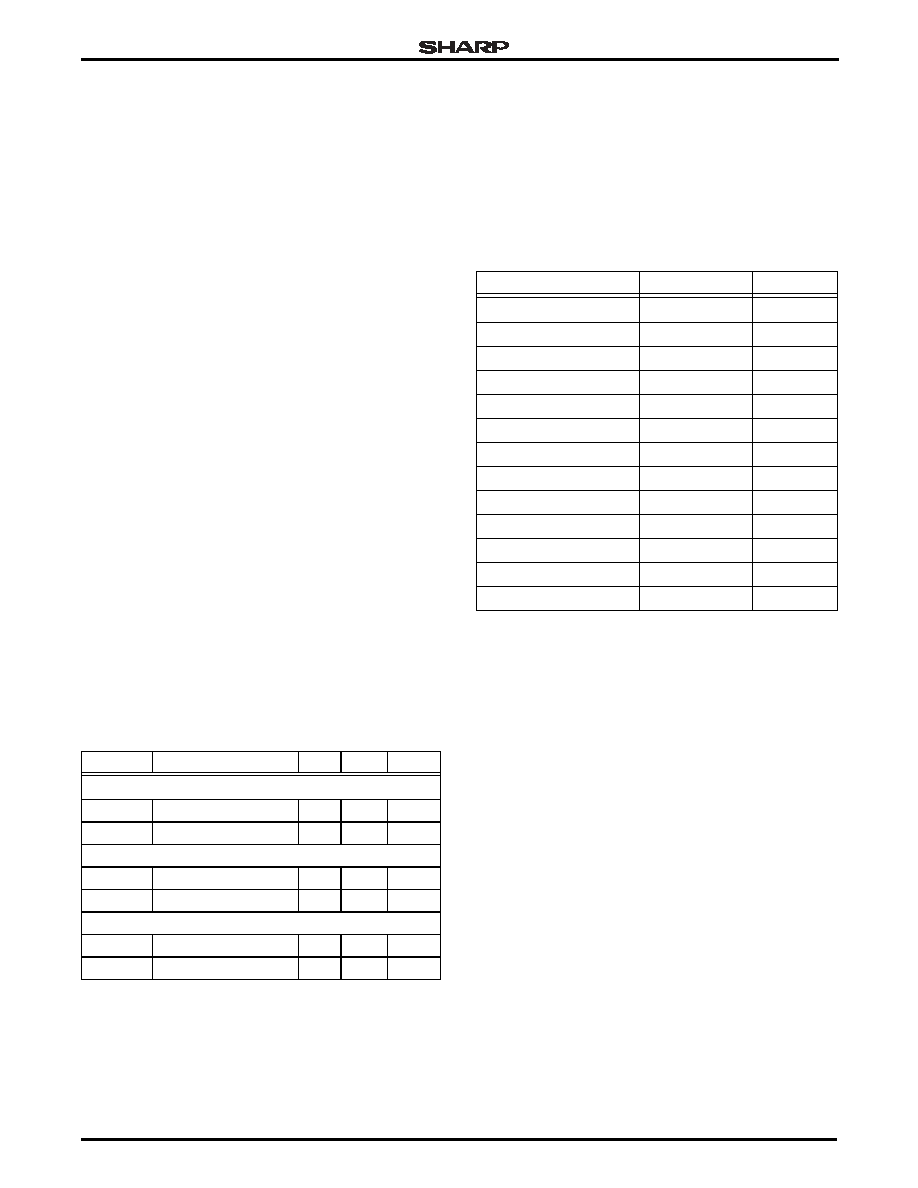
LH7A400
32-Bit System-on-Chip
36
8/27/03
Preliminary Data Sheet
CURRENT CONSUMPTION BY OPERATING MODE
Current consumption can depend on a number of
parameters. To make this data more usable, the values
presented in Table 7 were derived under the conditions
presented here.
Maximum Specified Value
The values specified in the MAXIMUM column were
determined using these operating characteristics:
∑ All IP blocks either operating or enabled at maximum
frequency and size configuration
∑ Core operating at maximum power configuration
∑ All voltages at maximum specified values
∑ Maximum specified ambient temperature.
Typical
The values in the TYPICAL column were determined
using a `typical' application under `typical' environmental
conditions and the following operating characteristics:
∑ LINUX operating system running from SDRAM
∑ UART and AC97 peripherals operating; all other
peripherals as needed by the OS
∑ LCD enabled with 320 ◊ 240 ◊ 16-bit color, 60 Hz
refresh rate, data in SDRAM
∑ I/O loads at nominal
∑ Cache enabled
∑ FCLK = 200 MHz; HCLK = 100 MHz; PCLK = 50 MHz
∑ All voltages at typical values
∑ Nominal case temperature.
PERIPHERAL CURRENT CONSUMPTION
In addition to the modal current consumption, Table
8 shows the typical current consumption for each of the
on-board peripheral blocks. The values were deter-
mined with the peripheral clock running at maximum
frequency, typical conditions, and no I/O loads. This
current is supplied by the 1.8 V power supply.
Table 7. Current Consumption by Mode
SYMBOL
PARAMETER
TYP.
MAX. UNITS
ACTIVE MODE
ICORE
Current drawn by core
132
180
mA
IIO
Current drawn by I/O
15
58
mA
HALT MODE (ALL PERIPHERALS DISABLED)
ICORE
Current drawn by core
40
44
mA
IIO
Current drawn by I/O
1
1
mA
STANDBY MODE (TYPICAL CONDITIONS ONLY)
ICORE
Current drawn by core
38
µ
A
IIO
Current drawn by I/O
4
µ
A
Table 8. Peripheral Current Consumption
PERIPHERAL
TYPICAL
UNITS
AC97
1.3
mA
UART (each)
1.0
mA
RTC
0.005
mA
Timers (each)
0.1
mA
LCD (+I/O)
5.4 (1.0)
mA
MMC
0.6
mA
SCI
23
mA
PWM (each)
<0.1
mA
BMI-SWI
1.0
mA
BMI-SBus
1.0
mA
SDRAM (+I/O)
1.5 (14.8)
mA
USB (+PLL)
5.6 (3.3)
mA
ACI
0.8
mA
32-Bit System-on-Chip
LH7A400
Preliminary Data Sheet
8/27/03
37
AC Specifications
All signals described in Table 9 relate to transi-
tions after a reference clock signal. The illustration in
Figure 6 represents all cases of these sets of mea-
surement parameters.
The reference clock signals in this design are:
∑ HCLK, internal System Bus clock (`C' in timing data)
∑ PCLK, Peripheral Bus clock
∑ SSPCLK, Synchronous Serial Port clock
∑ UARTCLK, UART Interface clock
∑ LCDDCLK, LCD Data clock from the
LCD Controller
∑ ACBITCLK, AC97 clock
∑ SCLK, Synchronous Memory clock.
All signal transitions are measured from the 50%
point of the clock to the 50% point of the signal.
For outputs from the LH7A400, tOVXXX (e.g. tOVA)
represents the amount of time for the output to become
valid from a valid address bus, or rising edge of the
peripheral clock. Maximum requirements for tOVXXX
are shown in Table 9.
The signal tOHXXX (e.g. tOHA) represents the
amount of time the output will be held valid from the valid
address bus, or rising edge of the peripheral clock. Min-
imum requirements for tOHXXX are listed in Table 9.
For Inputs, tISXXX (e.g. tISD) represents the amount
of time the input signal must be valid after a valid
address bus, or rising edge of the peripheral clock. Max-
imum requirements for tISXXX are shown in Table 9.
The signal tIHXXX (e.g. tIHD) represents the
amount of time the output must be held valid from the
valid address bus, or rising edge of the peripheral
clock. Minimum requirements are shown in Table 9.
Figure 6. LH7A400 Signal Timing
Table 9. AC Signal Characteristics
SIGNAL
TYPE
LOAD
SYMBOL
MIN.
MAX.
DESCRIPTION
ASYNCHRONOUS MEMORY INTERFACE SIGNALS (+ wait states
◊
C)
2
D[31:0]
Output
50 pF
tOVD
1C + 1 ns
Data Valid
tOHD
3C ≠ 7 ns
Data Hold
Input
tISD
3C ≠ 20 ns
Data Setup
tIHD
3C ≠ 3 ns
Data Hold
nCS[3:0]/CS[7:6]
Output
30 pF
tOVCSR
0 ns
Chip Select Valid (Read)
tOVCSW
1C
Chip Select Valid (Write)
tOHCS
3C ≠ 10 ns
Chip Select Hold
nWE[3:0] Output
30
pF
tOVWE
1C
Write Enable Valid
tOHWE
2C ≠ 10 ns
Write Enable Hold
nOE Output
30
pF
tOVOE
1C
Ouput Enable Valid
tOHOE
3C ≠ 10 ns
Ouput Enable Hold
SYNCHRONOUS MEMORY INTERFACE SIGNALS
SA[13:0]
Output
50 pF
tOVA
7.5 ns
Address Valid
SA[17:16]/SB[1:0]
Output
50 pF
tOVB
7.5 ns
Bank Select Valid
REFERENCE
CLOCK
OUTPUT
SIGNAL (O)
INPUT
SIGNAL (I)
tOVXXX
tOHXXX
tISXXX tIHXXX
7A400-28

LH7A400
32-Bit System-on-Chip
38
8/27/03
Preliminary Data Sheet
NOTES:
1. For Output Drive strength specifications, refer to Table 1.
2. `nC' in the MIN./MAX. columns indicates the number of system clock (HCLK) periods after valid address.
D[31:0]
Output
50 pF
tOVD
2 ns
7.5 ns
Data Valid
Input
tISD
2 ns
Data Setup
tIHD
1 ns
Data Hold
nCAS
Output
30 pF
tOVCA
2 ns
7.5 ns
CAS Valid
tOHCA
0.0 ns
CAS Hold
nRAS
Output
30 pF
tOVRA
2 ns
7.5 ns
RAS Valid
tOHRA
0.0 ns
RAS Hold
nSWE
Output
30 pF
tOVSDW
2 ns
7.5 ns
Write Enable Valid
tOHSDW
0.0 ns
Write Enable Hold
SCKE[1:0]
Output
30 pF
tOVC0
2 ns
7.5 ns
Clock Enable Valid
DQM[3:0]
Output
30 pF
tOVDQ
2 ns
7.5 ns
Data Mask Valid
nSCS[3:0] Output
30
pF
tOVSC
2 ns
7.5 ns
Synchronous Chip Select Valid
tOHSC
0.0 ns
Synchronous Chip Select Hold
PCMCIA INTERFACE SIGNALS (+ wait states
◊
C)
2
nPCREG
Output
30 pF
tOVDREG
1C
nREG Valid
tOHDREG
4C ≠ 5 ns
nREG Hold
D[31:0]
Output
50 pF
tOVD
1C
Data Valid
tOHD
4C ≠ 5 ns
Data Hold
Input
tISD
4C ≠ 15 ns
Data Setup Time
tIHD
1C
Data Hold Time
nPCCE1
Output
30 pF
tOVCE1
1C
Chip Enable 1 Valid
tOHCE1
4C ≠ 5 ns
Chip Enable 1 Hold
nPCCE2
Output
30 pF
tOVCE2
1C
Chip Enable 2 Valid
tOHCE2
4C ≠ 5 ns
Chip Enable 2 Hold
nPCOE
Output
30 pF
tOVOE
1C + 1 ns
Output Enable Valid
tOHOE
3C ≠ 5 ns
Output Enable Hold
nPCWE
Output
30 pF
tOVWE
1C + 1 ns
Write Enable Valid
tOHWE
3C ≠ 5 ns
Write Enable Hold
PCDIR
Output
30 pF
tOVPCD
1C
Card Direction Valid
tOHPCD
4C ≠ 5 ns
Card Direction Hold
MMC INTERFACE SIGNALS
MMCCMD
Output
100 pF
tOVCMD
3 ns
MMC Command Valid
tOHCMD
3 ns
MMC Command Hold
MMCDATA
Output
100 pF
tOVDAT
3 ns
MMC Data Valid
tOHDAT
3 ns
MMC Data Hold
MMCDATA
Input
tISDAT
5 ns
MMC Data Setup
tIHDAT
5 ns
MMC Data Hold
MMCCMD
Input
tISCMD
5 ns
MMC Command Setup
tIHCMD
5 ns
MMC Command Hold
AC97 INTERFACE SIGNALS
ACOUT
Output
30 pF
tOVAC97
15 ns
AC97 Output Valid
tOHAC97
10 ns
AC97 Output Hold
ACIN Input
tISAC97
10 ns
AC97 Input Setup
tIHAC97
2.5 ns
AC97 Input Hold
ACSYNC
Output
30 pF
tOVSYNCAC97
0 ns
15 ns
AC97 Synchronization Valid
tOHSYNCAC97
10 ns
AC97 Synchronization Hold
SYNCHRONOUS SERIAL PORT (SSP)
SSPFRM
Input
tISSSPFRM
14 ns
SSPFRM Input Valid
SSPTX
Output
50 pF
tOVSSPOUT
14 ns
SSP Transmit Valid
SSPRX
Input
tISSSPIN
14 ns
SSP Receive Setup
Table 9. AC Signal Characteristics (Cont'd)
SIGNAL
TYPE
LOAD
SYMBOL
MIN.
MAX.
DESCRIPTION

32-Bit System-on-Chip
LH7A400
Preliminary Data Sheet
8/27/03
39
Asynchronous Memory
Controller Waveforms
Figure 7 shows the waveform and timing for an
External Asynchronous Memory Write. Figure 8 shows
the waveform and timing for an External Asynchronous
Memory Read, with one Wait State.
Figure 7. External Asynchronous Memory Write
Figure 8. External Asynchronous Memory Read
HCLK
(See Note 2)
ADDRESS
DATA
A[27:0]
(See Note 1)
D[31:0]
nCSx, CSx
nWE[3:0]
tOVD
tOHD
tOVCSW
tOHCS
tOVWE
tOHWE
LH7A400-20
NOTES:
1. A[24:0] when SCI used.
2. HCLK is an internal signal, shown for reference only.
0
1
2
3
4
HCLK
(See Note)
ADDRESS
DATA
A[25:0]
D[31:0]
nCSx, CSx
nOE
tISD
tIHD
tOHCS
tOVCSR
tOVOE
tOHOE
LH7A400-21
NOTE: HCLK is an internal signal, shown for reference only.
0
1
2
3
LH7A400
32-Bit System-on-Chip
40
8/27/03
Preliminary Data Sheet
Synchronous Memory Controller Waveforms
Figure 9 shows the waveform and timing for a Syn-
chronous Burst Read (page already open). Figure 10
shows the waveform and timing for Synchronous mem-
ory to Activate a Bank and Write.
Figure 9. Synchronous Burst Read
Figure 10. Synchronous Bank Activate and Write
tSCLK
LH7A400-23
SA[13:0],
SB[1:0]
D[31:0]
NOTES:
1. SDRAMcmd is the combination of nRAS, nCAS, nSWE, and nSCSx.
2. tOVXXX represents tOVRA, tOVCA, tOVSVW, or tOVSC.
3. tOHXXX represents tOHRA, tOHCA, tOHSVW, or tOHSC.
4. nDQM is LOW.
5. SCKE is HIGH.
SCLK
SDRAMcmd
nDQM
tOVXXX
tOVA
tOHXXX
READ
BANK,
COLUMN
tOVA
tISD tIHD
DATA n
DATA n + 1
DATA n + 2
DATA n + 3
LH7A400-24
D[31:0]
SCLK
SCKE
SDRAMcmd
tSCLK
tOVC
tOVXXX
tOVA
tOHXXX
tOVA
NOTES:
1. SDRAMcmd is the combination of nRAS, nCAS, nSWE, and nSCSx.
2. tOVXXX represents tOVRA, tOVCA, tOVSVW, or tOVSC. Refer to the AC timing table.
3. tOHXXX represents tOHRA, tOHCA, tOHSVW, or tOHSC.
4. nDQM is LOW.
ACTIVE
WRITE
DATA
BANK,
ROW
BANK,
COLUMN
tOVD
tOHD
SA[13:0],
SB[1:0]
nDQM

32-Bit System-on-Chip
LH7A400
Preliminary Data Sheet
8/27/03
41
PC Card (PCMCIA) Waveforms
Figure 11 shows the waveforms and timing for a
PCMCIA Read Transfer, Figure 12 shows the wave-
forms and timing for a PCMCIA Write Transfer.
Figure 11. PCMCIA Read Transfer
tOVDREG
HCLK
A[25:0]
tOVPCD
tISD
tOHDREG
ADDRESS
PRECHARGE
TIME
(See Note 1)
ACCESS
TIME
(See Note 1)
HOLD
TIME
(See Note 1)
DATA
tIHD
tOVCEx
tOHCEx
LH7A400-11
nPCREG
nPCCEx
(See Note 2)
PCDIR
D[15:0]
nPCOE
NOTES:
1. Precharge time, access time, and hold
time are programmable wait-state times.
2.
nPCCE1
0
0
1
1
nPCCE2
0
1
0
1
TRANSFER TYPE
Common Memory
Attribute Memory
I/O
None
tOVWE
tOHWE

LH7A400
32-Bit System-on-Chip
42
8/27/03
Preliminary Data Sheet
Figure 12. PCMCIA Write Transfer
tOVDREG
HCLK
A[25:0]
tOVPCD
tOVD
tOVWE
tOHDREG
ADDRESS
PRECHARGE
TIME
(See Note 1)
ACCESS
TIME
(See Note 1)
HOLD
TIME
(See Note 1)
DATA
tOHD
tOHWE
tOVCEx
tOHCEx
LH7A400-12
nPCREG
nPCCEx
(See Note 2)
PCDIR
D[15:0]
nPCWE
NOTES:
1. Precharge time, access time, and hold
time are programmable wait-state times.
2.
nPCCE1
0
0
1
1
nPCCE2
0
1
0
1
TRANSFER TYPE
Common Memory
Attribute Memory
I/O
None
32-Bit System-on-Chip
LH7A400
Preliminary Data Sheet
8/27/03
43
MMC Interface Waveforms
Figure 13 shows the waveforms and timing for an
MMC command or data Write, and Figure 14 shows
the waveforms and timing for an MMC command or
data Read.
AC97 Interface Waveforms
Figure 15 shows the waveforms and timing for the
AC97 interface Data Setup and Hold.
Figure 13. MMC Command/Data Write
Figure 14. MMC Command/Data Read
Figure 15. AC97 Data Setup and Hold
tOVCMD
MMCCLK
MMCCMD
MMCDAT
tOHCMD
tOVDAT
tOHDAT
LH7A400-14
tISCMD
MMCCLK
MMCCMD
MMCDAT
tIHCMD
tISDAT tIHDAT
LH7A400-15
tOVAC97
AC97SYNC
AC97OUT
AC97IN
tISAC97 tIHAC97
tOHAC97
LH7A400-16
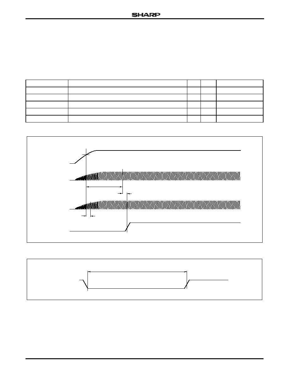
LH7A400
32-Bit System-on-Chip
44
8/27/03
Preliminary Data Sheet
Clock and State Controller (CSC)
Waveforms
Figure 16 shows the behavior of the LH7A400 when
coming out of Reset or Power On. Figure 17 shows exter-
nal reset timing, and Table 10 gives the timing parame-
ters. Figure 18 depicts signal timing following a Reset.
Figure 19 shows the recommended components for
the SHARP LH7A400 32.768 kHz external oscillator
circuit. Figure 20 shows the same for the 14.7456 MHz
external oscillator circuit. In both figures, the NAND
gate represents the internal logic of the chip.
NOTE: *VDDC = VDDCmin
Table 10. Reset AC Timing
PARAMETER
DESCRIPTION
MIN.
MAX.
UNIT
tOSC32
32 kHz Oscillator Stabilization Time after Power On*
550
ms
tPORH
nPOR Hold Time after tOSC32
0
ms
tOSC14
14.7456 MHz Oscillator Stabilization Time after Wake UP
4
ms
tPLLL
Phase Locked Loop Lockup Time
250
µ
s
tURESET/tPWRFL
nURESET/nPWRFL Pulse Width (once sampled LOW)
2
System Clock Cycles
Figure 16. Oscillator Start-up
Figure 17. External Reset
LH7A400-25
tOSC32
tOSC14
tPORH
VDDC
VDDCmin
XTAL32
nPOR
XTAL14
LH7A400-26
tURESET
tPWRFL
nURESET
nPWRFL
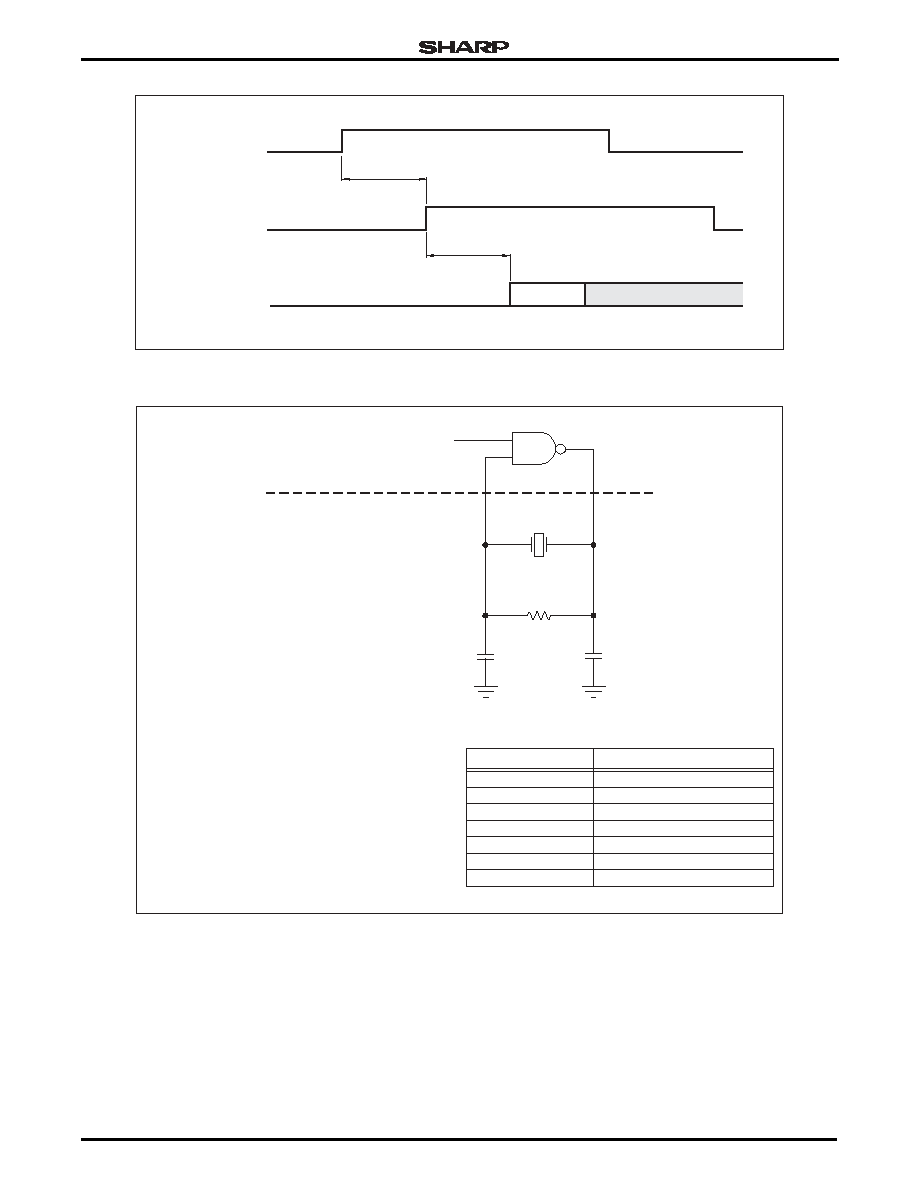
32-Bit System-on-Chip
LH7A400
Preliminary Data Sheet
8/27/03
45
Figure 18. Signal Timing After Reset
Figure 19. 32.768 kHz External Oscillator Components and Schematic
7.8125 ms
7.8125 ms
START UP
WAKEUP
(asynchronous)
CLKEN
HCLK
STABLE CLOCK
LH7A400-175
ENABLE
XTALIN
XTALOUT
GND
NOTES:
1. Y1 is a parallel-resonant type crystal. (See table)
2. The nominal values for C1 and C2 shown are for
a crystal specified at 12.5 pF load capacitance (CL).
3. The values for C1 and C2 are dependent upon
the cystal's specified load capacitance and PCB
stray capacitance.
4. R1 must be in the circuit.
5. Ground connections should be short and return
to the ground plane which is connected to the
processor's core ground pins.
6. Tolerance for R1, C1, C2 is
5%.
GND
32.768 kHz
18 M
LH7A400-187
PARAMETER
DESCRIPTION
32.768 kHz Crystal
Tolerance
Aging
Load Capacitance
ESR (MAX.)
Drive Level
Recommended Part
Parallel Mode
±30 ppm
±3 ppm
12.5 pF
50 k
1.0 µW (MAX.)
MTRON SX1555 or equivalent
C1
15 pF
C2
18 pF
R1
Y1
INTERNAL TO
THE LH7A400
EXTERNAL TO
THE LH7A400
RECOMMENDED CRYSTAL SPECIFICATIONS

LH7A400
32-Bit System-on-Chip
46
8/27/03
Preliminary Data Sheet
Figure 20. 14.7456 MHz External Oscillator Components and Schematic
ENABLE
XTALIN
XTALOUT
GND
NOTES:
1. Y1 is a parallel-resonant type crystal. (See table)
2. The nominal values for C1 and C2 shown are for
a crystal specified at 18 pF load capacitance (CL).
3. The values for C1 and C2 are dependent upon
the cystal's specified load capacitance and PCB
stray capacitance.
4. R1 must be in the circuit.
5. Ground connections should be short and return
to the ground plane which is connected to the
processor's core ground pins.
6. Tolerance for R1, C1, C2 is
5%.
GND
14.7456 MHz
1 M
LH7A400-188
C1
18 pF
C2
22 pF
R1
Y1
INTERNAL TO
THE LH7A400
EXTERNAL TO
THE LH7A400
PARAMETER
DESCRIPTION
14.7456 MHz Crystal
Tolerance
Stability
Aging
Load Capacitance
ESR (MAX.)
Drive Level
Recommended Part
(AT-Cut) Parallel Mode
±50 ppm
±100 ppm
±5 ppm
18 pF
40
100 µW (MAX.)
MTRON SX2050 or equivalent
RECOMMENDED CRYSTAL SPECIFICATIONS

32-Bit System-on-Chip
LH7A400
Preliminary Data Sheet
8/27/03
47
Printed Circuit Board Layout Practices
LH7A400 POWER SUPPLY DECOUPLING
The LH7A400 has separate power and ground pins
for different internal circuitry sections. The VDD and
VSS pins supply power to I/O buffers, while VDDC and
VSSC supply power to the core logic, and VDDA/VSSA
supply analog power to the PLLs.
Each of the VDD and VDDC pins must be provided
with a low impedance path to the corresponding board
power supply. Likewise, the VSS and VSSC pins must
be provided with a low impedance path to the board
ground.
Each power supply must be decoupled to ground
using at least one 0.1
µ
F high frequency capacitor
located as close as possible to a VDDx, VSSx pin pair
on each of the four sides of the chip. If room on the cir-
cuit board allows, add one 0.01
µ
F high frequency
capacitor near each VDDx, VSSx pair on the chip.
To be effective, the capacitor leads and associated
circuit board traces connecting to the chip VDDx, VSSx
pins must be kept to less than half an inch (12.7 mm)
per capacitor lead. There must be one bulk 10
µ
F
capacitor for each power supply placed near one side
of the chip.
REQUIRED LH7A400 PLL, VDDA, VSSA FILTER
The VDDA pins supplies power to the chip PLL cir-
cuitry. VSSA is the ground return path for the PLL cir-
cuit. These pins must have a low-pass filter attached as
shown in Figure 21.
The Schottky diode shown in the schematic must
have a low forward drop specification to allow VDDA to
quickly transition through the entire input voltage range.
The power pin VDDA path must be a single wire
from the IC package pin to the high frequency capaci-
tor, then to the low frequency capacitor, and finally
through the series resistor to the board power supply.
The distance from the IC pin to the high frequency
capacitor must be kept as short as possible.
Similarly, the VSSA path is from the IC pin to the
high frequency capacitor, then to the low frequency
capacitor, keeping the distance from the IC pin to the
high frequency cap as short as possible.
UNUSED INPUT SIGNAL CONDITIONING
Floating input signals can cause excessive power
consumption. Unused inputs without internal pull-up or
pull-down resistors should be pulled up or down exter-
nally, to tie the signal to its inactive state.
Some GPIO signals may default to inputs. If the pins
that carry these signals are unused, software can pro-
gram these signals as outputs, eliminating the need for
pull-ups or pull-downs. Power consumption may be
higher than expected until software completes pro-
gramming the GPIO. Some LH7A400 inputs have inter-
nal pull-ups or pull-downs. If unused, these inputs do
not require external conditioning.
OTHER CIRCUIT BOARD LAYOUT PRACTICES
All outputs have fast rise and fall times. Printed cir-
cuit trace interconnection length must therefore be
reduced to minimize overshoot, undershoot and reflec-
tions caused by transmission line effects of these fast
output switching times. This recommendation particu-
larly applies to the address and data buses.
When considering capacitance, calculations must
consider all device loads and capacitances due to the
circuit board traces. Capacitance due to the traces will
depend upon a number of factors, including the trace
width, dielectric material the circuit board is made from
and proximity to ground and power planes.
Attention to power supply decoupling and printed cir-
cuit board layout becomes more critical in systems with
higher capacitive loads. As these capacitive loads
increase, transient currents in the power supply and
ground return paths also increase.
Note that the VSSA pin specifically does not have a connec-
tion to the circuit board ground. The LH7A400 PLL circuit has
an internal DC ground connection to VSS (GND), so the ex-
ternal VSSA pin must NOT be connected to the circuit board
ground, but only to the filter components.
CAUTION
Figure 21. VDDA, VSSA Filter Circuit
LH7A400-189
VDDA
VDDC
VSSA
22 µF
100
VDDC
(SOURCE)
0.1 µF
+
LH7A400
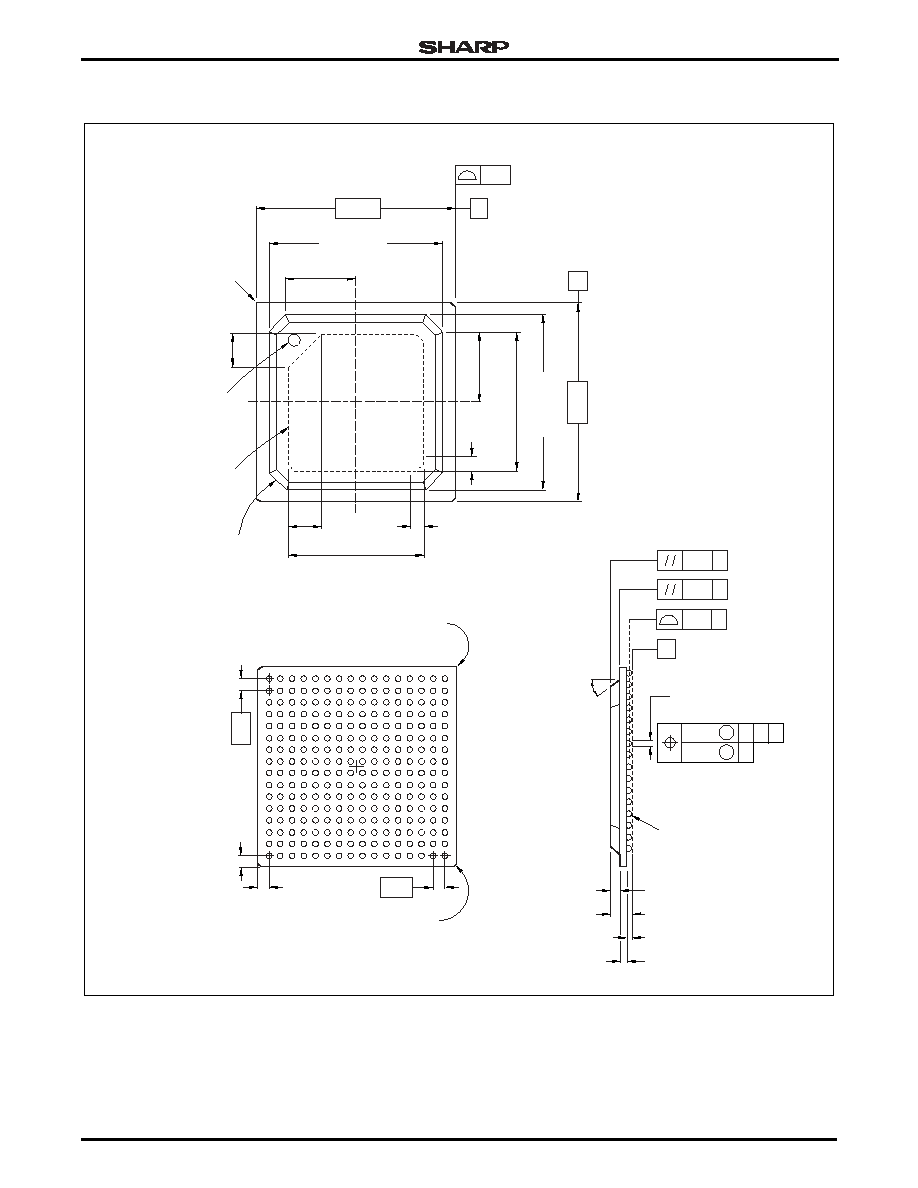
LH7A400
32-Bit System-on-Chip
48
8/27/03
Preliminary Data Sheet
PACKAGE SPECIFICATIONS
Figure 22. 256-Ball PBGA Package Specification
1.00
1.00 REF.
15.00
+0.70
-0.05
15.00
+0.70
-0.05
+0.10
-0.10
6.00
2.90
6.00
2.90
11.64 MAX.
1.21 TYP.
1.21 TYP
.
11.64 MAX.
BOTTOM VIEW
(256 solder balls)
SIDE VIEW
TOP VIEW
1.00 REF
.
0.50 R, 3 PLACES
NOTE: Dimensions in mm.
C
C A
C
B
0.30 M
0.50
0.10 M
C
0.15
0.80 ±0.05
0.40 ±0.10
1.76 ±0.21
SEATING PLANE
0.56 ±0.06
1.00
B
A1 BALL
PAD CORNER
15 13
11
9
7
5
3
A
B
C
D
E
F
G
H
J
K
L
M
N
P
R
T
1
16
30∞
TYP.
14
12
10
8
6
4
2
A
(4X)
0.20
C
0.25
C
0.35
17.00
17.00
256-BALL PBGA
A1 BALL
PAD
CORNER
A1 BALL PAD
INDICATOR, 1.0 DIA.
AVAILABLE
MARKING
AREA
45
∞
CHAMFER
4 PLACES
256PBGA
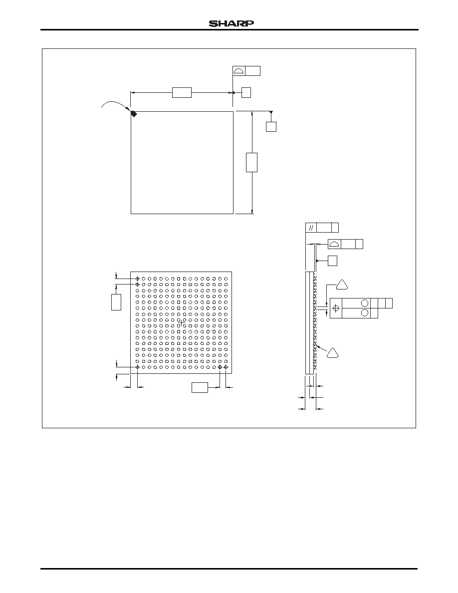
32-Bit System-on-Chip
LH7A400
Preliminary Data Sheet
8/27/03
49
Figure 23. 256-Ball CABGA Package Specification
0.80
1.0
1.0
BOTTOM VIEW
(256 solder balls)
SIDE VIEW
TOP VIEW
C
C
5
A
C
B
0.15 M
0.46 TYP.
0.08 M
C
0.12
0.36 ±0.04
0.70 ±0.05
SEATING PLANE
1.70 MAX.
0.80
B
15
13 11
9
7
5
3
A
B
C
D
E
F
G
H
J
K
L
M
N
P
R
T
1
14
12
10
8
16
6
4
2
A
(4X)
0.10
C
0.10
14.00
14.00
A1 BALL
PAD CORNER
256-BALL CABGA
256CABGA
6
NOTE: Dimensions in mm.
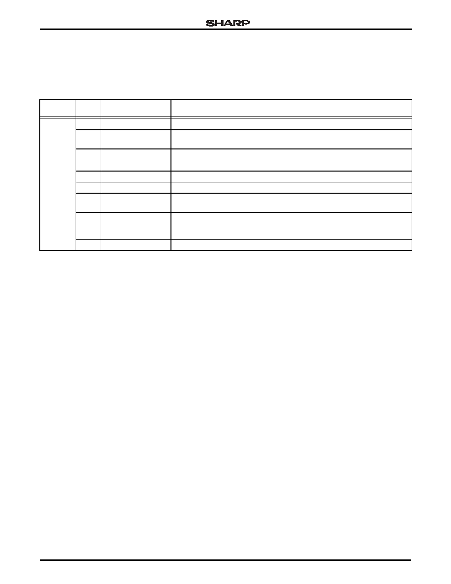
LH7A400
32-Bit System-on-Chip
50
8/27/03
Preliminary Data Sheet
CONTENT REVISIONS
This document contains the following changes to
content, causing it to differ from previous versions.
Table 11. Record of Revisions
DATE
PAGE
NO.
PARAGRAPH OR
ILLUSTRATION
SUMMARY OF CHANGES
8-19-2003
1
Features
256-ball CABGA package added
3-11
Table 1
CABGA Pins added; VDDA1/VDDA2 combined to VDDA; VSSA1/VSSA2
combined to VSSA
12
Table 3
Signal ordering corrected
12-18
Table 4
Table title added to differentiate between PBGA and CABGA packages
18-24
Table 5
CABGA numerical pin list table added
39
Figure 7 and Figure 8
`CSx' added to figures
44
Table 10 and
Figure 16
tOSC14 added to both table and figure; XTAL14 added to figure;
tPLLL added to table
45-47
Figures 19-21 and
Printed Circuit Board
Layout Practices
Figures and text added
49
Figure 23
Figure added for CABGA package

LH7A400
32-Bit System-on-Chip
©2003 by SHARP Corporation
Reference Code SMA01012
SPECIFICATIONS ARE SUBJECT TO CHANGE WITHOUT NOTICE.
Suggested applications (if any) are for standard use; See Important Restrictions for limitations on special applications. See Limited
Warranty for SHARP's product warranty. The Limited Warranty is in lieu, and exclusive of, all other warranties, express or implied.
ALL EXPRESS AND IMPLIED WARRANTIES, INCLUDING THE WARRANTIES OF MERCHANTABILITY, FITNESS FOR USE AND
FITNESS FOR A PARTICULAR PURPOSE, ARE SPECIFICALLY EXCLUDED. In no event will SHARP be liable, or in any way responsible,
for any incidental or consequential economic or property damage.
NORTH AMERICA
EUROPE
JAPAN
SHARP Microelectronics of the Americas
5700 NW Pacific Rim Blvd.
Camas, WA 98607, U.S.A.
Phone: (1) 360-834-2500
Fax: (1) 360-834-8903
www.sharpsma.com
SHARP Microelectronics Europe
Division of Sharp Electronics (Europe) GmbH
Sonninstrasse 3
20097 Hamburg, Germany
Phone: (49) 40-2376-2286
Fax: (49) 40-2376-2232
www.sharpsme.com
SHARP Corporation
Electronic Components & Devices
22-22 Nagaike-cho, Abeno-Ku
Osaka 545-8522, Japan
Phone: (81) 6-6621-1221
Fax: (81) 6117-725300/6117-725301
www.sharp-world.com
TAIWAN
SINGAPORE
KOREA
SHARP Electronic Components
(Taiwan) Corporation
8F-A, No. 16, Sec. 4, Nanking E. Rd.
Taipei, Taiwan, Republic of China
Phone: (886) 2-2577-7341
Fax: (886) 2-2577-7326/2-2577-7328
SHARP Electronics (Singapore) PTE., Ltd.
438A, Alexandra Road, #05-01/02
Alexandra Technopark,
Singapore 119967
Phone: (65) 271-3566
Fax: (65) 271-3855
SHARP Electronic Components
(Korea) Corporation
RM 501 Geosung B/D, 541
Dohwa-dong, Mapo-ku
Seoul 121-701, Korea
Phone: (82) 2-711-5813 ~ 8
Fax: (82) 2-711-5819
CHINA
HONG KONG
SHARP Microelectronics of China
(Shanghai) Co., Ltd.
28 Xin Jin Qiao Road King Tower 16F
Pudong Shanghai, 201206 P.R. China
Phone: (86) 21-5854-7710/21-5834-6056
Fax: (86) 21-5854-4340/21-5834-6057
Head Office:
No. 360, Bashen Road,
Xin Development Bldg. 22
Waigaoqiao Free Trade Zone Shanghai
200131 P.R. China
Email: smc@china.global.sharp.co.jp
SHARP-ROXY (Hong Kong) Ltd.
3rd Business Division,
17/F, Admiralty Centre, Tower 1
18 Harcourt Road, Hong Kong
Phone: (852) 28229311
Fax: (852) 28660779
www.sharp.com.hk
Shenzhen Representative Office:
Room 13B1, Tower C,
Electronics Science & Technology Building
Shen Nan Zhong Road
Shenzhen, P.R. China
Phone: (86) 755-3273731
Fax: (86) 755-3273735