Advance Data Sheet
1
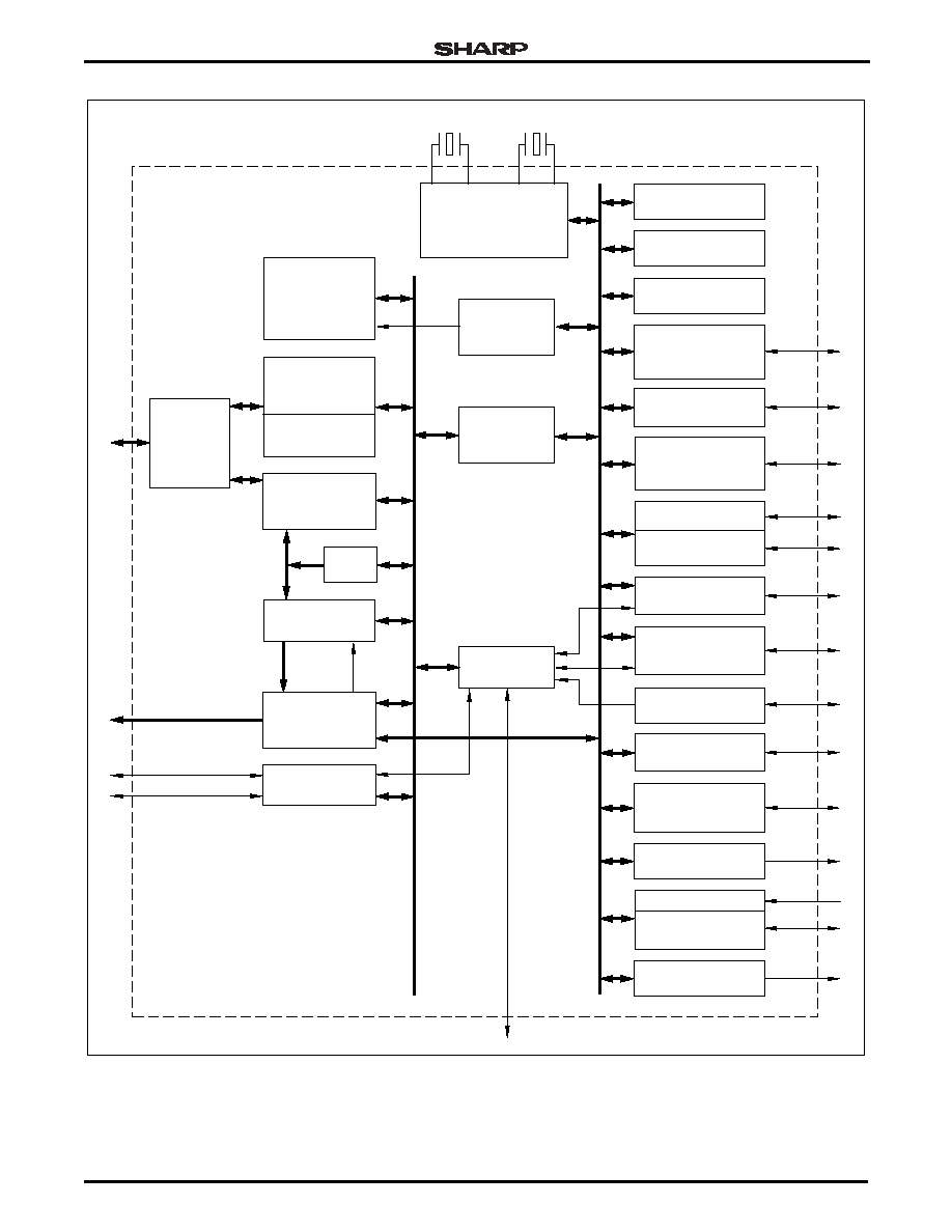
LH7A404
Advance Data Sheet
32-Bit System-on-Chip
FEATURES
∑ ARM922TTM Core:
≠ 32-bit ARM9TDMITM RISC Core (200 MHz)
≠ 16KB Cache: 8KB Instruction Cache and 8KB
Data Cache
≠ MMU (Windows CETM Enabled)
∑ 80KB On-Chip Memory
∑ Vectored Interrupt Controller
∑ External Bus Interface
≠ 100 MHz
≠ Asynchronous SRAM/ROM/Flash
≠ Synchronous DRAM/Flash
≠ PCMCIA
≠ Compact Flash
∑ Clock and Power Management
≠ 32.768 kHz and 14.7456 MHz Oscillators
≠ Programmable PLL
∑ Low Power Modes
≠ Run (200 mA), Halt, Standby (35
µ
A)
∑ Programmable LCD Controller
≠ Up to 1,024 ◊ 768 Resolution
≠ Supports STN, Color STN, HR-TFT, TFT
≠ Up to 64 k-Colors and 15 Gray Shades
∑ 10 Channel, 10-bit A/D Converter
≠ Touch Screen Controller
≠ Brownout Detector
∑ DMA (12 Channels)
≠ External DMA Channels
≠ AAC (AC97)
≠ MMC
≠ USB
∑ USB Host and Device Interface (USB1.1)
∑ Synchronous Serial Port (SSP)
≠ Motorola SPITM
≠ Texas Instruments SSI
≠ National MICROWIRETM
∑ PS/2 Keyboard/Mouse Interface (KMI)
∑ Three Programmable Timers
∑ Three UARTs
≠ Classic IrDA (115 kbit/s)
∑ Smart Card Interface (ISO7816)
∑ Four Pulse Width Modulators (PWMs)
∑ MultiMediaCard Interface with Secure Digital
(MMC 2.11/SD 1.0)
∑ AAC (AC97) Codec Interface
∑ Smart Battery Monitor Interface
∑ Real Time Clock (RTC)
∑ Up to 64 General Purpose I/O Channels
∑ Programmable Interrupt Controller
∑ Watchdog Timer
∑ JTAG Debug Interface and Boundary Scan
∑ Operating Voltage
≠ 1.8 V Core
≠ 3.3 V Input/Output (1.8 V I/O Optional*)
∑ Temperature
≠ 0∞C to +70∞C Commercial
≠ -40∞C to +85∞C Industrial (With Clock Frequency
Reduction*)
∑ 324-Ball PBGA Package
DESCRIPTION
The advent of 3G technology opens the door for a
wide range of Multimedia applications in mobile infor-
mation appliances. These appliances require high pro-
cessing performance and low power consumption. The
LH7A404 is designed from the ground up to provide
high processing performance, low power consumption,
and a high level of integration.
The LH7A404 contains a high performance 32-bit
ARM922T Core. Power consumption is reduced by the
high level of integration, 80KB on-chip SRAM, fully static
design, power management unit, low voltage operation
(1.8 V Core, 1.8 V or 3.3 V I/O) and on-chip PLL.
Motorola SPI is a trademark of Motorola, Inc.
National Semiconductor MICROWIRE is a trademark of
National Semiconductor Corporation.
ARM922T and ARM 9TDMI are trademarks of Advanced RISC Machines
(ARM) Ltd.
Windows CE is a trademark of Microsoft Corporation.
NOTE: *Under development. Results pending further
characterization.
LH7A404
32-Bit System-on-Chip
4
Advance Data Sheet
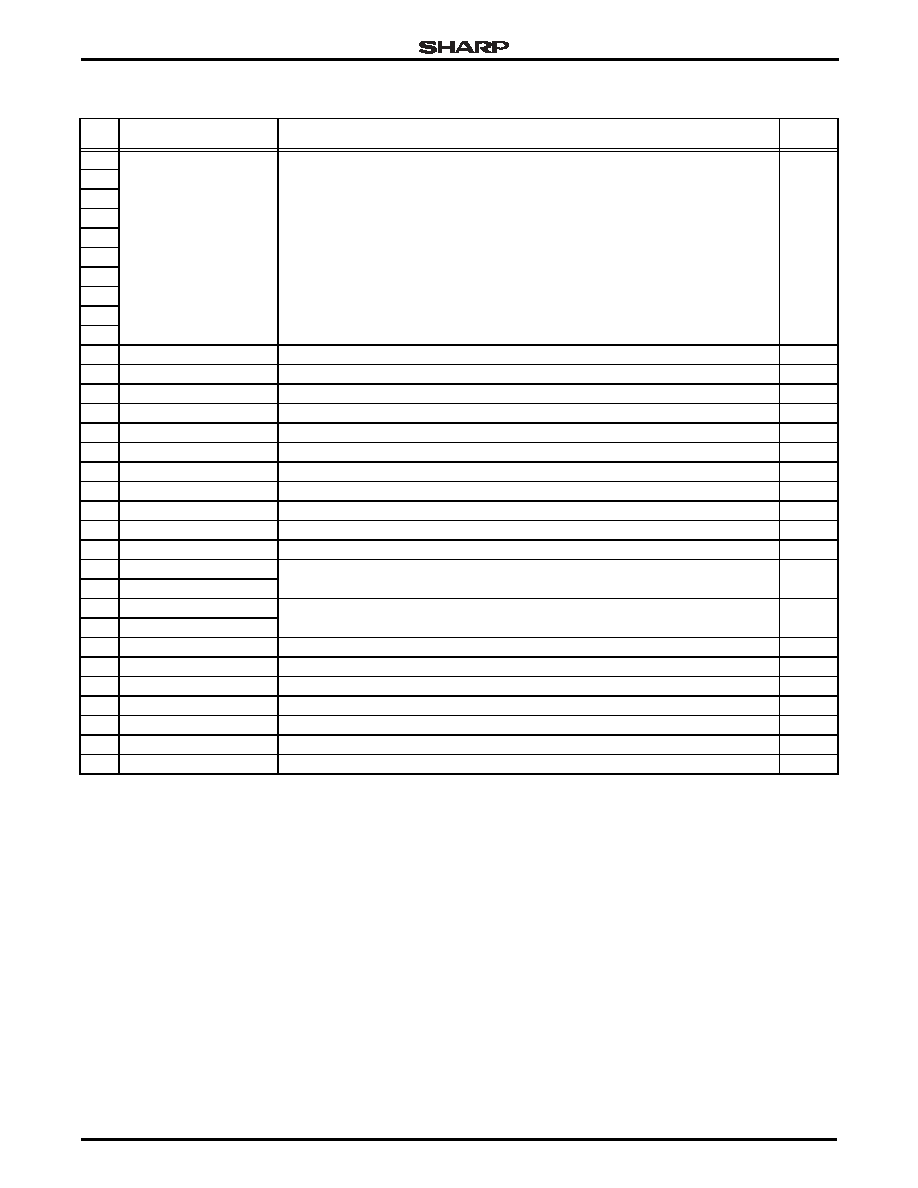
G2
VSSC
Core Ground
M2
AA6
AA15
P21
K21
F21
B17
B10
B5
AA17 VDDA1
Analog Power for PLL1
AB17 VSSA1
Analog Ground for PLL1
AA18 VDDA2
Analog Power for PLL2
AB18 VSSA2
Analog Ground for PLL2
AB16 VDDA3
Analog Power for A/D, Touch Screen Controller
AB13 VSSA3
Analog Ground for A/D, Touch Screen Controller
D3
nPOR
Power on Reset
E3
nURESET
User Reset
D4
WAKEUP
Wake Up
E1
nPWRFL
Power Fail Signal
2 mA
C2
nEXTPWR
External Power
AA16 XTALIN
14.7456 MHz Crystal Oscillator pins. To drive the device from an external clock source, XTALIN
can be used while XTALOUT is left unconnected.
Y16
XTALOUT
AA21 XTAL32IN
32.768 kHz Real Time Clock, Crystal Oscillator pins. To drive the device from an external clock
source, XTAL32IN can be used while XTAL32OUT is left unconnected.
Y20
XTAL32OUT
L3
PGMCLK
Programmable Clock (14.7456 MHz MAX.)
8 mA
AB22 nCS0
Asynchronous Memory Chip Select 0 (ROM/Flash)
16 mA
N13
nCS1
Asynchronous Memory Chip Select 1
16 mA
Y21
nCS2
Asynchronous Memory Chip Select 2
16 mA
W20
nCS3/nMMCSEL
Asynchronous Memory Chip Select 3 and MMC Select
16 mA
Y22
nCS6
Asynchronous Memory Chip Select 6
16 mA
W21
nCS7
Asynchronous Memory Chip Select 7
16 mA
Table 1. Functional Pin List (Cont'd)
BGA
SIGNAL
DESCRIPTION
OUTPUT
DRIVE