 | –≠–ª–µ–∫—Ç—Ä–æ–Ω–Ω—ã–π –∫–æ–º–ø–æ–Ω–µ–Ω—Ç: LHF00L11 | –°–∫–∞—á–∞—Ç—å:  PDF PDF  ZIP ZIP |

Æ
Integrated Circuits Group
LHF00L11
Flash Memory
32M (2MB ◊ 16)
(Model No.: LHF00L11)
Spec No.: EL112031A
Issue Date: March 15, 2004
P
RODUCT
S
PECIFICATIONS
LHF00L11
∑ Handle this document carefully for it contains material protected by international copyright law. Any reproduction,
full or in part, of this material is prohibited without the express written permission of the company.
∑ When using the products covered herein, please observe the conditions written herein and the precautions outlined in
the following paragraphs. In no event shall the company be liable for any damages resulting from failure to strictly
adhere to these conditions and precautions.
(1) The products covered herein are designed and manufactured for the following application areas. When using the
products covered herein for the equipment listed in Paragraph (2), even for the following application areas, be sure
to observe the precautions given in Paragraph (2). Never use the products for the equipment listed in Paragraph
(3).
∑ Office electronics
∑ Instrumentation and measuring equipment
∑ Machine tools
∑ Audiovisual equipment
∑ Home appliance
∑ Communication equipment other than for trunk lines
(2) Those contemplating using the products covered herein for the following equipment which demands high
reliability, should first contact a sales representative of the company and then accept responsibility for
incorporating into the design fail-safe operation, redundancy, and other appropriate measures for ensuring
reliability and safety of the equipment and the overall system.
∑ Control and safety devices for airplanes, trains, automobiles, and other transportation equipment
∑ Mainframe computers
∑ Traffic control systems
∑ Gas leak detectors and automatic cutoff devices
∑ Rescue and security equipment
∑ Other safety devices and safety equipment, etc.
(3) Do not use the products covered herein for the following equipment which demands extremely high performance
in terms of functionality, reliability, or accuracy.
∑ Aerospace equipment
∑ Communications equipment for trunk lines
∑ Control equipment for the nuclear power industry
∑ Medical equipment related to life support, etc.
(4) Please direct all queries and comments regarding the interpretation of the above three Paragraphs to a sales
representative of the company.
∑ Please direct all queries regarding the products covered herein to a sales representative of the company.
Rev. 2.45

LHF00L11 1
Rev. 2.45
CONTENTS
PAGE
0.75mm pitch 48-Ball CSP Pinout ............................. 3
Pin Descriptions.......................................................... 4
Memory Map .............................................................. 5
Identifier Codes and OTP Address
for Read Operation ............................................. 6
OTP Block Address Map for OTP Program............... 7
Bus Operation............................................................. 8
Command Definitions ................................................ 9
Functions of Block Lock and Block Lock-Down...... 11
Block Locking State Transitions
upon Command Write........................................ 11
Block Locking State Transitions
upon WP# Transition........................................ 12
Status Register Definition......................................... 13
PAGE
1 Electrical Specifications ........................................ 14
1.1 Absolute Maximum Ratings........................... 14
1.2 Operating Conditions ..................................... 14
1.2.1 Capacitance.............................................. 15
1.2.2 AC Input/Output Test Conditions............ 15
1.2.3 DC Characteristics................................... 16
1.2.4 AC Characteristics
- Read-Only Operations............................ 18
1.2.5 AC Characteristics
- Write Operations .................................... 20
1.2.6 Reset Operations...................................... 22
1.2.7 Block Erase, Full Chip Erase,
Program and OTP Program Performance. 23
2 Related Document Information ............................. 24
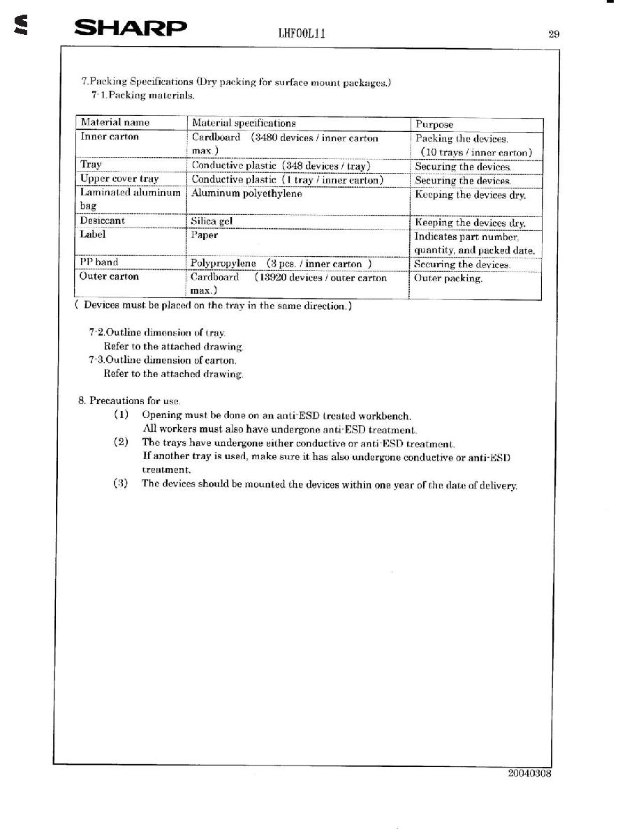
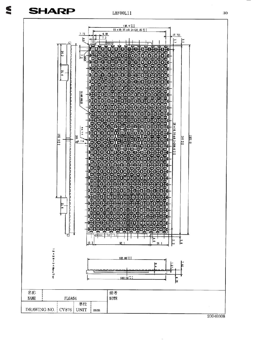
3 Package and packing specification........................ 25

LHF00L11 2
LHF00L11
32Mbit (2Mbit
◊16)
Flash MEMORY
32-M density with 16-bit I/O Interface
Read Operation
∑ 90ns
Low Power Operation
∑ 2.7V Read and Write Operations
∑ V
CCQ
for Input/Output Power Supply Isolation
∑ Automatic Power Savings Mode reduces I
CCR
in Static Mode
Enhanced Code + Data Storage
∑ 5
µs Typical Erase/Program Suspends
OTP (One Time Program) Block
∑ 4-Word Factory-Programmed Area
∑ 4-Word User-Programmable Area
Operating Temperature -40
∞C to +85∞C
CMOS Process (P-type silicon substrate)
Flexible Blocking Architecture
∑ Eight 4-Kword Parameter Blocks
∑ One 32-Kword Block
∑ Thirty-one 64-Kword Blocks
∑ Bottom Parameter Location
Enhanced Data Protection Features
∑ Individual Block Lock and Block Lock-Down with
Zero-Latency
∑ All blocks are locked at power-up or device reset.
∑ Absolute Protection with V
PP
V
PPLK
∑ Block Erase, Full Chip Erase, Word Program Lockout
during Power Transitions
Automated Erase/Program Algorithms
∑ 3.0V Low-Power
10µs/Word (Typ.)
Programming
∑ 12.0V No Glue Logic 9
µs/Word (Typ.)
Production Programming and 0.8s Erase (Typ.)
Cross-Compatible Command Support
∑ Basic Command Set
∑ Common Flash Interface (CFI)
Extended Cycling Capability
∑ Minimum 100,000 Block Erase Cycles
0.75mm pitch 48-Ball CSP
ETOX
TM*
Flash Technology
Not designed or rated as radiation hardened
The product is a low power, high density, low cost, nonvolatile read/write storage solution for a wide range of applications.
The product can operate at V
CC
=2.7V-3.6V and V
PP
=1.65V-3.6V or 11.7V-12.3V. Its low voltage operation capability
greatly extends battery life for portable applications.
The memory array block architecture utilizes Enhanced Data Protection features, which provides maximum flexibility for
safe nonvolatile code and data storage.
Special OTP (One Time Program) block provides an area to store permanent code such as an unique number.
* ETOX is a trademark of Intel Corporation.
Rev. 2.45
LHF00L11 3
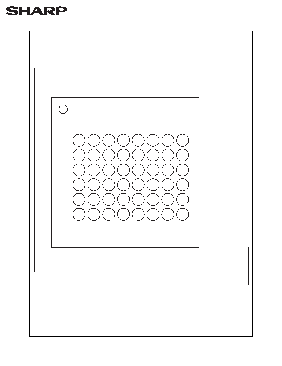
A
8
WP#
A
18
WE#
RST#
NC
DQ
11
DQ
12
DQ
6
DQ
13
DQ
4
V
CC
3
4
5
6
7
V
PP
A
19
A
6
A
9
DQ
2
DQ
5
DQ
3
A
4
A
7
A
17
A
2
A
1
CE#
DQ
8
DQ
0
DQ
9
GND
OE#
DQ
10
A
B
C
D
E
F
A
5
A
3
A
0
DQ
1
A
20
8
0.75mm pitch
48-BALL CSP
PINOUT
7mm x 7mm
TOP VIEW
A
13
A
14
A
10
A
12
DQ
14
DQ
15
V
CCQ
GND
DQ
7
1
2
A
11
A
15
A
16
Figure 1. 0.75mm pitch 48-Ball CSP Pinout
Rev. 2.45

LHF00L11 4
Table 1. Pin Descriptions
Symbol
Type
Name and Function
A
20
-A
0
INPUT
ADDRESS INPUTS: Inputs for addresses.
DQ
15
-DQ
0
INPUT/
OUTPUT
DATA INPUTS/OUTPUTS: Inputs data and commands during CUI (Command User
Interface) write cycles, outputs data during memory array, status register, query code,
identifier code reads. Data pins float to high-impedance (High Z) when the chip or
outputs are deselected. Data is internally latched during an erase or program cycle.
CE#
INPUT
CHIP ENABLE: Activates the device's control logic, input buffers, decoders and sense
amplifiers. CE#-high (V
IH
) deselects the device and reduces power consumption to
standby levels.
RST#
INPUT
RESET: When low (V
IL
), RST# resets internal automation and inhibits write operations
which provides data protection. RST#-high (V
IH
) enables normal operation. After
power-up or reset mode, the device is automatically set to read array mode. RST# must
be low during power-up/down.
OE#
INPUT
OUTPUT ENABLE: Gates the device's outputs during a read cycle.
WE#
INPUT
WRITE ENABLE: Controls writes to the CUI and array blocks. Addresses and data are
latched on the rising edge of CE# or WE# (whichever goes high first).
WP#
INPUT
WRITE PROTECT: When WP# is V
IL
, locked-down blocks cannot be unlocked. Erase
or program operation can be executed to the blocks which are not locked and not locked-
down. When WP# is V
IH
, lock-down is disabled.
V
PP
INPUT/SUPPLY
MONITORING POWER SUPPLY VOLTAGE: V
PP
is not used for power supply pin.
With V
PP
V
PPLK
, block erase, full chip erase, program or OTP program cannot be
executed and should not be attempted.
Applying 12.0V±0.3V to V
PP
provides fast erasing or fast programming mode. In this
mode, V
PP
is power supply pin. Applying 12.0V±0.3V to V
PP
during erase/program can
only be done for a maximum of 1,000 cycles on each block. V
PP
may be connected to
12.0V±0.3V for a total of 80 hours maximum. Use of this pin at 12.0V+0.3V beyond
these limits may reduce block cycling capability or cause permanent damage.
V
CC
SUPPLY
DEVICE POWER SUPPLY (2.7V-3.6V): With V
CC
V
LKO
, all write attempts to the
flash memory are inhibited. Device operations at invalid V
CC
voltage (see DC
Characteristics) produce spurious results and should not be attempted.
V
CCQ
SUPPLY
INPUT/OUTPUT POWER SUPPLY (2.7V-3.6V): Power supply for all input/output
pins.
GND
SUPPLY
GROUND: Do not float any ground pins.
NC
NO CONNECT: Lead is not internally connected; it may be driven or floated.
Rev. 2.45
LHF00L11 5
64-Kword Block 39
64-Kword Block 38
64-Kword Block 37
64-Kword Block 36
64-Kword Block 35
64-Kword Block 34
64-Kword Block 33
64-Kword Block 32
64-Kword Block 31
64-Kword Block 30
64-Kword Block 29
64-Kword Block 28
64-Kword Block 27
64-Kword Block 26
64-Kword Block 25
64-Kword Block 24
64-Kword Block 23
64-Kword Block 22
64-Kword Block 21
64-Kword Block 20
64-Kword Block 19
64-Kword Block 18
64-Kword Block 17
64-Kword Block 16
64-Kword Block 15
64-Kword Block 14
64-Kword Block 13
64-Kword Block 12
64-Kword Block 11
64-Kword Block 10
64-Kword Block 9
[A
20
-
A
0
]
010000
01FFFF
020000
02FFFF
030000
03FFFF
040000
04FFFF
050000
05FFFF
060000
06FFFF
070000
07FFFF
080000
08FFFF
090000
09FFFF
0A0000
0AFFFF
0B0000
0BFFFF
0C0000
0CFFFF
0D0000
0DFFFF
0E0000
0EFFFF
0F0000
0FFFFF
100000
10FFFF
110000
11FFFF
120000
12FFFF
130000
13FFFF
140000
14FFFF
150000
15FFFF
170000
17FFFF
180000
18FFFF
190000
19FFFF
1A0000
1AFFFF
1B0000
1BFFFF
1C0000
1CFFFF
1D0000
1DFFFF
1E0000
1EFFFF
160000
16FFFF
32-Kword Block 8
4-Kword Block 7
4-Kword Block 6
4-Kword Block 5
4-Kword Block 4
4-Kword Block 3
4-Kword Block 2
4-Kword Block 1
4-Kword Block 0
000000
000FFF
001000
001FFF
002000
002FFF
003000
003FFF
004000
004FFF
005000
005FFF
006000
006FFF
007000
007FFF
008000
00FFFF
1F0000
1EFFFF
Figure 2. Memory Map (Bottom Parameter)
Rev. 2.45
LHF00L11 6
NOTES:
1. Block Address = The beginning location of a block address. DQ
15
-DQ
2
are reserved for future implementation.
2. OTP-LK=OTP Block Lock configuration.
3. OTP=OTP Block data.
Table 2. Identifier Codes and OTP Address for Read Operation
Code
Address
[A
20
-A
0
]
Data
[DQ
15
-DQ
0
]
Notes
Manufacturer Code
Manufacturer Code
000000H
00B0H
Device Code
Device Code
000001H
00A1H
Block Lock Configuration
Code
Block is Unlocked
Block
Address
+ 2
DQ
0
= 0
1
Block is Locked
DQ
0
= 1
1
Block is not Locked-Down
DQ
1
= 0
1
Block is Locked-Down
DQ
1
= 1
1
OTP
OTP Lock
000080H
OTP-LK
2
OTP 000081-000088H
OTP
3
Rev. 2.45

LHF00L11 7
Customer Programmable Area Lock Bit (DQ
1
)
Factory Programmed Area Lock Bit (DQ
0
)
Customer Programmable Area
Factory Programmed Area
Reserved for Future Implementation
000080H
000081H
000084H
000085H
000088H
(DQ
15
-DQ
2)
Figure 3. OTP Block Address Map for OTP Program
(The area outside 80H~88H cannot be used.)
[
A
20
-A
0
]
Rev. 2.45

LHF00L11 8
NOTES:
1. Refer to DC Characteristics. When V
PP
V
PPLK
, memory contents can be read, but cannot be altered.
2. X can be V
IL
or V
IH
for control pins and addresses, and V
PPLK
or V
PPH1/2
for V
PP
.
Refer to DC Characteristics for V
PPLK
and V
PPH1/2
voltages.
3. RST# at GND±0.2V ensures the lowest power consumption.
4. Command writes involving block erase, full chip erase, program or OTP program are
reliably executed when V
PP
=V
PPH1/2
and V
CC
=2.7V-3.6V.
5. Refer to Table 4 for valid D
IN
during a write operation.
6. Never hold OE# low and WE# low at the same timing.
7. Refer to Appendix of LHF00LXX series for more information about query code.
Table 3. Bus Operation
(1, 2)
Mode
Notes
RST#
CE#
OE#
WE#
Address
V
PP
DQ
15-0
Read Array
6
V
IH
V
IL
V
IL
V
IH
X
X
D
OUT
Output Disable
V
IH
V
IL
V
IH
V
IH
X
X
High Z
Standby
V
IH
V
IH
X
X
X
X
High Z
Reset
3
V
IL
X
X
X
X
X
High Z
Read Identifier
Codes/OTP
6
V
IH
V
IL
V
IL
V
IH
See
Table 2
X
See
Table 2
Read Query
6,7
V
IH
V
IL
V
IL
V
IH
See
Appendix
X
See
Appendix
Read Status
Register
6
V
IH
V
IL
V
IL
V
IH
X
X
D
OUT
Write
4,5,6
V
IH
V
IL
V
IH
V
IL
X
V
PPH1/2
D
IN
Rev. 2.45
LHF00L11 9
NOTES:
1. Bus operations are defined in Table 3.
2. All addresses which are written at the first bus cycle should be the same as the addresses which are written at the second
bus cycle.
X=Any valid address within the device.
IA=Identifier codes address (See Table 2).
QA=Query codes address. Refer to Appendix of LHF00LXX series for details.
BA=Address within the block being erased, set/cleared block lock bit or set block lock-down bit.
WA=Address of memory location for the Program command.
OA=Address of OTP block to be read or programmed (See Figure 3).
3. ID=Data read from identifier codes. (See Table 2).
QD=Data read from query database. Refer to Appendix of LHF00LXX series for details.
SRD=Data read from status register. See Table 8 for a description of the status register bits.
WD=Data to be programmed at location WA. Data is latched on the rising edge of WE# or CE# (whichever
goes high first) during command write cycles.
OD=Data within OTP block. Data is latched on the rising edge of WE# or CE# (whichever goes high first)
during command write cycles.
4. Following the Read Identifier Codes/OTP command, read operations access manufacturer code, device code, block lock
configuration code and the data within OTP block (See Table 2).
The Read Query command is available for reading CFI (Common Flash Interface) information.
5. Block erase, full chip erase or program cannot be executed when the selected block is locked. Unlocked block can be
erased or programmed when RST# is V
IH
.
6. Either 40H or 10H are recognized by the CUI (Command User Interface) as the program setup.
7. If the program operation and the erase operation are both suspended, the suspended program operation will be resumed
first.
8. Full chip erase and OTP program operations can not be suspended. The OTP Program command can not be accepted
while the block erase operation is being suspended.
Table 4. Command Definitions
(10)
Command
Bus
Cycles
Req'd
Notes
First Bus Cycle
Second Bus Cycle
Oper
(1)
Addr
(2)
Data
Oper
(1)
Addr
(2)
Data
(3)
Read Array
1
Write
X
FFH
Read Identifier Codes/OTP
2
4
Write
X
90H
Read
IA or OA
ID or OD
Read Query
2
4
Write
X
98H
Read
QA
QD
Read Status Register
2
Write
X
70H
Read
X
SRD
Clear Status Register
1
Write
X
50H
Block Erase
2
5
Write
BA
20H
Write
BA
D0H
Full Chip Erase
2
5, 8
Write
X
30H
Write
X
D0H
Program
2
5,6
Write
WA
40H or
10H
Write
WA
WD
Block Erase and
Program Suspend
1
7, 8
Write
X
B0H
Block Erase and
Program Resume
1
7, 8
Write
X
D0H
Set Block Lock Bit
2
Write
BA
60H
Write
BA
01H
Clear Block Lock Bit
2
9
Write
BA
60H
Write
BA
D0H
Set Block Lock-down Bit
2
Write
BA
60H
Write
BA
2FH
OTP Program
2
8
Write
OA
C0H
Write
OA
OD
Rev. 2.45

LHF00L11 10
9. Following the Clear Block Lock Bit command, block which is not locked-down is unlocked when WP# is V
IL
. When
WP# is V
IH
, lock-down bit is disabled and the selected block is unlocked regardless of lock-down configuration.
10. Commands other than those shown above are reserved by SHARP for future device implementations and should not be
used.
Rev. 2.45
LHF00L11 11
NOTES:
1. DQ
0
=1: a block is locked; DQ
0
=0: a block is unlocked.
DQ
1
=1: a block is locked-down; DQ
1
=0: a block is not locked-down.
2. Erase and program are general terms, respectively, to express: block erase, full chip erase and
program operations.
3. At power-up or device reset, all blocks default to locked state and are not locked-down, that is,
[001] (WP#=0) or [101] (WP#=1), regardless of the states before power-off or reset operation.
4. When WP# is driven to V
IL
in [110] state, the state changes to [011] and the blocks are
automatically locked.
5. OTP (One Time Program) block has the lock function which is different from those described
above.
NOTES:
1. "Set Lock" means Set Block Lock Bit command, "Clear Lock" means Clear Block Lock Bit
command and "Set Lock-down" means Set Block Lock-Down Bit command.
2. When the Set Block Lock-Down Bit command is written to the unlocked block (DQ
0
=0), the
corresponding block is locked-down and automatically locked at the same time.
3. "No Change" means that the state remains unchanged after the command written.
4. In this state transitions table, assumes that WP# is not changed and fixed V
IL
or V
IH
.
Table 5. Functions of Block Lock
(5)
and Block Lock-Down
Current State
Erase/Program Allowed
(2)
State
WP#
DQ
1
(1)
DQ
0
(1)
State Name
[000]
0
0
0
Unlocked
Yes
[001]
(3)
0
0
1
Locked
No
[011]
0
1
1
Locked-down
No
[100]
1
0
0
Unlocked
Yes
[101]
(3)
1
0
1
Locked
No
[110]
(4)
1
1
0
Lock-down Disable
Yes
[111]
1
1
1
Lock-down Disable
No
Table 6. Block Locking State Transitions upon Command Write
(4)
Current State
Result after Lock Command Written (Next State)
State
WP#
DQ
1
DQ
0
Set Lock
(1)
Clear Lock
(1)
Set Lock-down
(1)
[000]
0
0
0
[001]
No Change
[011]
(2)
[001]
0
0
1
No Change
(3)
[000]
[011]
[011]
0
1
1
No Change
No Change
No Change
[100]
1
0
0
[101]
No Change
[111]
(2)
[101]
1
0
1
No Change
[100]
[111]
[110]
1
1
0
[111]
No Change
[111]
(2)
[111]
1
1
1
No Change
[110]
No Change
Rev. 2.45

LHF00L11 12
NOTES:
1. "WP#=0
1" means that WP# is driven to V
IH
and "WP#=1
0" means that WP# is driven to
V
IL
.
2. State transition from the current state [011] to the next state depends on the previous state.
3. When WP# is driven to V
IL
in [110] state, the state changes to [011] and the blocks are
automatically locked.
4. In this state transitions table, assumes that lock configuration commands are not written in
previous, current and next state.
Table 7. Block Locking State Transitions upon WP# Transition
(4)
Previous State
Current State
Result after WP# Transition (Next State)
State
WP#
DQ
1
DQ
0
WP#=0
1
(1)
WP#=1
0
(1)
-
[000]
0
0
0
[100]
-
-
[001]
0
0
1
[101]
-
[110]
(2)
[011]
0
1
1
[110]
-
Other than [110]
(2)
[111]
-
-
[100]
1
0
0
-
[000]
-
[101]
1
0
1
-
[001]
-
[110]
1
1
0
-
[011]
(3)
-
[111]
1
1
1
-
[011]
Rev. 2.45

LHF00L11 13
Table 8. Status Register Definition
R
R
R
R
R
R
R
R
15
14
13
12
11
10
9
8
WSMS
BESS
BEFCES
POPS
VPPS
PSS
DPS
R
7
6
5
4
3
2
1
0
SR.15 - SR.8 = RESERVED FOR FUTURE
ENHANCEMENTS (R)
SR.7 = WRITE STATE MACHINE STATUS (WSMS)
1 = Ready
0 = Busy
SR.6 = BLOCK ERASE SUSPEND STATUS (BESS)
1 = Block Erase Suspended
0 = Block Erase in Progress/Completed
SR.5 = BLOCK ERASE AND FULL CHIP ERASE
STATUS (BEFCES)
1 = Error in Block Erase or Full Chip Erase
0 = Successful Block Erase or Full Chip Erase
SR.4 = PROGRAM AND
OTP PROGRAM STATUS (POPS)
1 = Error in Program or OTP Program
0 = Successful Program or OTP Program
SR.3 = V
PP
STATUS (VPPS)
1 = V
PP
LOW Detect, Operation Abort
0 = V
PP
OK
SR.2 = PROGRAM SUSPEND
STATUS (PSS)
1 = Program Suspended
0 = Program in Progress/Completed
SR.1 = DEVICE PROTECT STATUS (DPS)
1 = Erase or Program Attempted on a
Locked Block, Operation Abort
0 = Unlocked
SR.0 = RESERVED FOR FUTURE ENHANCEMENTS (R)
NOTES:
Status Register indicates the status of the WSM (Write State
Machine).
Check SR.7 to determine block erase, full chip erase,
program or OTP program completion. SR.6 - SR.1 are invalid
while SR.7="0".
If both SR.5 and SR.4 are "1"s after a block erase, full chip
erase, program, set/clear block lock bit, set block lock-down
bit attempt, an improper command sequence was entered.
SR.3 does not provide a continuous indication of V
PP
level.
The WSM interrogates and indicates the V
PP
level only after
Block Erase, Full Chip Erase, Program or OTP Program
command sequences. SR.3 is not guaranteed to report
accurate feedback when V
PP
V
PPH1
, V
PPH2
or V
PPLK
.
SR.1 does not provide a continuous indication of block lock
bit. The WSM interrogates the block lock bit only after Block
Erase, Full Chip Erase, Program or OTP Program command
sequences. It informs the system, depending on the attempted
operation, if the block lock bit is set. Reading the block lock
configuration codes after writing the Read Identifier Codes/
OTP command indicates block lock bit status.
SR.15 - SR.8 and SR.0 are reserved for future use and should
be masked out when polling the status register.
Rev. 2.45

LHF00L11 14
1 Electrical Specifications
1.1 Absolute Maximum Ratings
*
Operating Temperature
During Read, Erase and Program ...-40
∞C to +85∞C
(1)
Storage Temperature
During under Bias............................... -40
∞C to +85∞C
During non Bias................................ -65
∞C to +125∞C
Voltage On Any Pin (except V
CC
, V
CCQ
and V
PP
)
............................................... -0.5V to V
CCQ
+0.5V
(2)
V
CC
and V
CCQ
Supply Voltage .......... -0.2V to +3.9V
(2)
V
PP
Supply Voltage .................... -0.2V to +12.6V
(2, 3, 4)
Output Short Circuit Current ........................... 100mA
(5)
*WARNING: Stressing the device beyond the "Absolute
Maximum Ratings" may cause permanent
damage. These are stress ratings only. Operation
beyond the "Operating Conditions" is not
recommended and extended exposure beyond the
"Operating Conditions" may affect device
reliability.
NOTES:
1. Operating temperature is for extended temperature
product defined by this specification.
2. All specified voltages are with respect to GND.
Minimum DC voltage is -0.5V on input/output pins and
-0.2V on V
CC
, V
CCQ
and V
PP
pins. During transitions,
this level may undershoot to -2.0V for periods <20ns.
Maximum DC voltage on input/output pins is
V
CC
+0.5V which, during transitions, may overshoot to
V
CC
+2.0V for periods <20ns.
3. Maximum DC voltage on V
PP
may overshoot to
+13.0V for periods <20ns.
4. V
PP
erase/program voltage is normally 2.7V-3.6V.
Applying 11.7V-12.3V to V
PP
during erase/program
can be done for a maximum of 1,000 cycles on each
block. V
PP
may be connected to 11.7V-12.3V for a
total of 80 hours maximum.
5. Output shorted for no more than one second. No more
than one output shorted at a time.
Rev. 2.45
1.2 Operating Conditions
NOTES:
1. See DC Characteristics tables for voltage range-specific specification.
2. Applying V
PP
=11.7V-12.3V during a erase or program can be done for a maximum of 1,000 cycles on each block. A
permanent connection to V
PP
=11.7V-12.3V is not allowed and can cause damage to the device.
Parameter
Symbol
Min.
Typ.
Max.
Unit
Notes
Operating Temperature
T
A
-40
+25
+85
∞C
V
CC
Supply Voltage
V
CC
2.7
3.0
3.6
V
1
I/O Supply Voltage
V
CCQ
2.7
3.0
3.6
V
1
V
PP
Voltage when Used as a Logic Control
V
PPH1
1.65
3.0
3.6
V
1
V
PP
Supply Voltage
V
PPH2
11.7
12.0
12.3
V
1, 2
Block Erase Cycling: V
PP
=V
PPH1
100,000
Cycles
Block Erase Cycling: V
PP
=V
PPH2
, 80 hrs.
1,000
Cycles
Maximum V
PP
hours at V
PPH2
80
Hours
LHF00L11 15
TEST POINTS
V
CCQ
/2
V
CCQ
/2
INPUT
V
CCQ
0.0
OUTPUT
AC test inputs are driven at V
CCQ
(min) for a Logic "1" and 0.0V for a Logic "0".
Input timing begins, and output timing ends at V
CCQ
/2. Input rise and fall times (10% to 90%) < 5ns.
Worst case speed conditions are when V
CC
=V
CC
(min).
DEVICE
UNDER
TEST
RL=3.3K
CL
V
CCQ
(min)/2
OUT
CL Includes Jig
Capacitances.
1N914
Figure 5. Transient Equivalent Testing Load Circuit
Table 9. Test Configuration Capacitance Loading Value
Test Configuration
C
L
(pF)
V
CC
=2.7V-3.6V
50
1.2.2 AC Input/Output Test Conditions
1.2.1 Capacitance
(1)
(T
A
=
+25∞C, f=1MHz)
NOTE:
1. Sampled, not 100% tested.
Parameter
Symbol
Condition
Min.
Typ.
Max.
Unit
Input Capacitance
C
IN
V
IN
=0.0V
4
7
pF
Output Capacitance
C
OUT
V
OUT
=0.0V
6
10
pF
Figure 4. Transient Input/Output Reference Waveform for V
CC
=2.7V-3.6V
Rev. 2.45

LHF00L11 16
Rev. 2.45
1.2.3 DC Characteristics
V
CC
=2.7V-3.6V
Symbol
Parameter
Notes
Min.
Typ.
Max.
Unit
Test Conditions
I
LI
Input Load Current
1
-1.0
+1.0
µA
V
CC
=V
CC
Max.,
V
CCQ
=V
CCQ
Max.,
V
IN
/V
OUT
=V
CCQ
or
GND
I
LO
Output Leakage Current
1
-1.0
+1.0
µA
I
CCS
V
CC
Standby Current
1,7
4
10
µA
V
CC
=V
CC
Max.,
CE#=RST#=
V
CCQ
±0.2V,
WP#=V
CCQ
or GND
I
CCAS
V
CC
Automatic Power Savings
Current
1,4,7
4
10
µA
V
CC
=V
CC
Max.,
CE#=GND±0.2V,
WP#=V
CCQ
or GND
I
CCD
V
CC
Reset Current
1,7
4
10
µA
RST#=GND±0.2V
I
CCR
V
CC
Read Current
1,7
17
mA
V
CC
=V
CC
Max.,
CE#=V
IL
,
OE#=V
IH
,
f=5MHz
I
CCW
V
CC
Program Current
1,5,7
20
60
mA
V
PP
=V
PPH1
1,5,7
10
20
mA
V
PP
=V
PPH2
I
CCE
V
CC
Block Erase,
Full Chip Erase Current
1,5,7
10
30
mA
V
PP
=V
PPH1
1,5,7
4
10
mA
V
PP
=V
PPH2
I
CCWS
I
CCES
V
CC
Program or
Block Erase Suspend Current
1,2,7
10
200
µA
CE#=V
IH
I
PPS
I
PPR
V
PP
Standby or Read Current
1,6,7
2
5
µA
V
PP
V
CC
I
PPW
V
PP
Program Current
1,5,6,7
2
5
µA
V
PP
=V
PPH1
1,5,6,7
10
30
mA
V
PP
=V
PPH2
I
PPE
V
PP
Block Erase,
Full Chip Erase Current
1,5,6,7
2
5
µA
V
PP
=V
PPH1
1,5,6,7
5
15
mA
V
PP
=V
PPH2
I
PPWS
V
PP
Program
Suspend Current
1,6,7
2
5
µA
V
PP
=V
PPH1
1,6,7
10
200
µA
V
PP
=V
PPH2
I
PPES
V
PP
Block Erase Suspend Current
1,6,7
2
5
µA
V
PP
=V
PPH1
1,6,7
10
200
µA
V
PP
=V
PPH2
LHF00L11 17
NOTES:
1. All currents are in RMS unless otherwise noted. Typical values are the reference values at V
CC
=3.0V, V
CCQ
=3.0V and
T
A
=+25
∞C unless V
CC
is specified.
2. I
CCWS
and I
CCES
are specified with the device de-selected. If read or program is executed while in block erase suspend
mode, the device's current draw is the sum of I
CCES
and I
CCR
or I
CCW
. If read is executed while in program suspend
mode, the device's current draw is the sum of I
CCWS
and I
CCR
.
3. Block erase, full chip erase, program and OTP program are inhibited when V
PP
V
PPLK
, and not guaranteed in the range
between V
PPLK
(max.) and V
PPH1
(min.), between V
PPH1
(max.) and V
PPH2
(min.), and above V
PPH2
(max.).
4. The Automatic Power Savings (APS) feature automatically places the device in power save mode after read cycle
completion. Standard address access timings (t
AVQV
) provide new data when addresses are changed.
5. Sampled, not 100% tested.
6. V
PP
is not used for power supply pin. With V
PP
V
PPLK
, block erase, full chip erase, program and OTP program cannot be
executed and should not be attempted.
Applying 12.0V±0.3V to V
PP
provides fast erasing or fast programming mode. In this mode, V
PP
is power supply pin and
supplies the memory cell current for block erasing and programming. Use similar power supply trace widths and layout
considerations given to the V
CC
power bus.
Applying 12.0V±0.3V to V
PP
during erase/program can only be done for a maximum of 1,000 cycles on each block. V
PP
may be connected to 12.0V±0.3V for a total of 80 hours maximum.
7. For all pins other than those shown in test conditions, input level is V
CCQ
or GND.
V
IL
Input Low Voltage
5
-0.4
0.4
V
V
IH
Input High Voltage
5
2.4
V
CCQ
+ 0.4
V
V
OL
Output Low Voltage
5
0.2
V
V
CC
=V
CC
Min.,
V
CCQ
=V
CCQ
Min.,
I
OL
=100
µA
V
OH
Output High Voltage
5
V
CCQ
-0.2
V
V
CC
=V
CC
Min.,
V
CCQ
=V
CCQ
Min.,
I
OH
=-100µA
V
PPLK
V
PP
Lockout during Normal
Operations
3,5,6
0.4
V
V
PPH1
V
PP
during Block Erase, Full Chip
Erase, Program or OTP Program
Operations
6
1.65
3.0
3.6
V
V
PPH2
V
PP
during Block Erase, Full Chip
Erase, Program or OTP Program
Operations
6
11.7
12.0
12.3
V
V
LKO
V
CC
Lockout Voltage
1.5
V
V
CC
=2.7V-3.6V
Symbol
Parameter
Notes
Min.
Typ.
Max.
Unit
Test Conditions
DC Characteristics (Continued)
Rev. 2.45
LHF00L11 18
1.2.4 AC Characteristics - Read-Only Operations
(1)
NOTES:
1. See AC input/output reference waveform for timing measurements and maximum allowable input slew rate.
2. Sampled, not 100% tested.
3. OE# may be delayed up to t
ELQV
t
GLQV
after the falling edge of CE# without impact to t
ELQV
.
V
CC
=2.7V-3.6V, T
A
=-40
∞C to +85∞C
Symbol
Parameter
Notes
Min.
Max.
Unit
t
AVAV
Read Cycle Time
90
ns
t
AVQV
Address to Output Delay
90
ns
t
ELQV
CE# to Output Delay
3
90
ns
t
GLQV
OE# to Output Delay
3
20
ns
t
PHQV
RST# High to Output Delay
150
ns
t
EHQZ
, t
GHQZ
CE# or OE# to Output in High Z, Whichever Occurs First
2
20
ns
t
ELQX
CE# to Output in Low Z
2
0
ns
t
GLQX
OE# to Output in Low Z
2
0
ns
t
OH
Output Hold from First Occurring Address, CE# or OE# change
2
0
ns
Rev. 2.45
LHF00L11 19
t
AVQV
t
EHQZ
t
GHQZ
t
ELQV
t
PHQV
t
GLQV
t
OH
V
IH
V
IL
V
IH
V
IL
V
IH
V
IL
V
IH
V
IL
V
OH
V
OL
V
IH
V
IL
(P)
(D/Q)
(W)
(G)
(E)
(A)
A
20-0
DQ
15-0
CE#
OE#
WE#
RST#
High Z
t
ELQX
VALID
OUTPUT
VALID
ADDRESS
t
GLQX
t
AVAV
Figure 6. AC Waveform for Read Operations
Rev. 2.45

LHF00L11 20
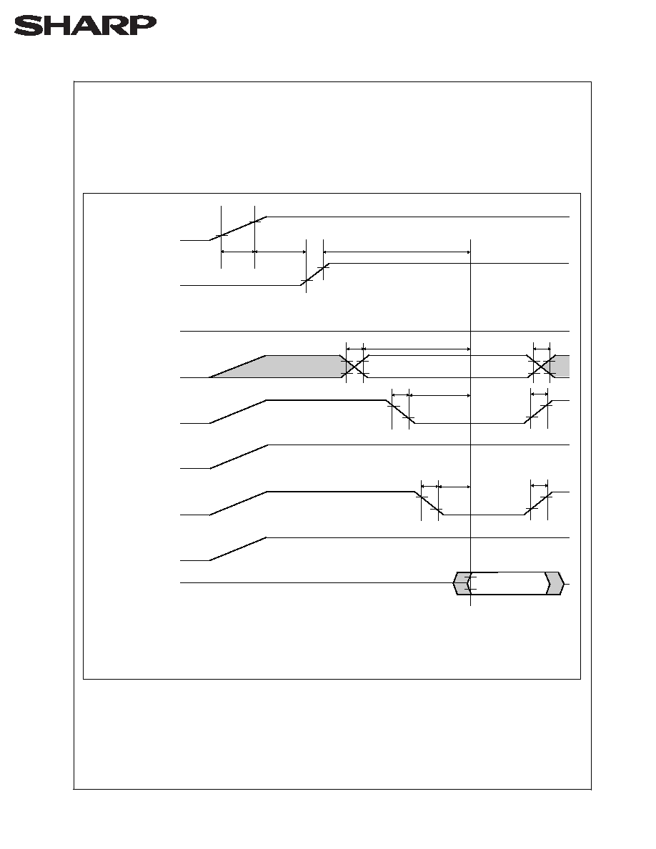
1.2.5 AC Characteristics - Write Operations
(1), (2)
NOTES:
1. The timing characteristics for reading the status register during block erase, full chip erase, program and OTP program
operations are the same as during read-only operations. Refer to AC Characteristics for read-only operations.
2. A write operation can be initiated and terminated with either CE# or WE#.
3. Sampled, not 100% tested.
4. Write pulse width (t
WP
) is defined from the falling edge of CE# or WE# (whichever goes low last) to the rising edge of
CE# or WE# (whichever goes high first). Hence, t
WP
=t
WLWH
=t
ELEH
=t
WLEH
=t
ELWH
.
5. Write pulse width high (t
WPH
) is defined from the rising edge of CE# or WE# (whichever goes high first) to the falling
edge of CE# or WE# (whichever goes low last). Hence, t
WPH
=t
WHWL
=t
EHEL
=t
WHEL
=t
EHWL
.
6. V
PP
should be held at V
PP
=V
PPH1/2
until determination of block erase, full chip erase, program or OTP program success
(SR.1/3/4/5=0).
7. t
WHR0
(t
EHR0
) after the Read Query or Read Identifier Codes/OTP command=t
AVQV
+100ns.
8. Refer to Table 4 for valid address and data for block erase, full chip erase, program, OTP program or lock bit
configuration.
V
CC
=2.7V-3.6V, T
A
=-40
∞C to +85∞C
Symbol
Parameter
Notes
Min.
Max.
Unit
t
AVAV
Write Cycle Time
90
ns
t
PHWL
(t
PHEL
)
RST# High Recovery to WE# (CE#) Going Low
3
150
ns
t
ELWL
(t
WLEL
)
CE# (WE#) Setup to WE# (CE#) Going Low
0
ns
t
WLWH
(t
ELEH
)
WE# (CE#) Pulse Width
4
60
ns
t
DVWH
(t
DVEH
)
Data Setup to WE# (CE#) Going High
8
40
ns
t
AVWH
(t
AVEH
)
Address Setup to WE# (CE#) Going High
8
50
ns
t
WHEH
(t
EHWH
)
CE# (WE#) Hold from WE# (CE#) High
0
ns
t
WHDX
(t
EHDX
)
Data Hold from WE# (CE#) High
0
ns
t
WHAX
(t
EHAX
)
Address Hold from WE# (CE#) High
0
ns
t
WHWL
(t
EHEL
)
WE# (CE#) Pulse Width High
5
30
ns
t
SHWH
(t
SHEH
)
WP# High Setup to WE# (CE#) Going High
3
0
ns
t
VVWH
(t
VVEH
)
V
PP
Setup to WE# (CE#) Going High
3
200
ns
t
WHGL
(t
EHGL
)
Write Recovery before Read
30
ns
t
QVSL
WP# High Hold from Valid SRD
3, 6
0
ns
t
QVVL
V
PP
Hold from Valid SRD
3, 6
0
ns
t
WHR0
(t
EHR0
)
WE# (CE#) High to SR.7 Going "0"
3, 7
t
AVQV
+
50
ns
Rev. 2.45

LHF00L11 21
t
AVAV
t
AVWH
(t
AVEH
)
t
WHAX
(t
EHAX
)
t
ELWL
(t
WLEL
)
t
PHWL
(t
PHEL
)
t
WLWH
t
WHWL
(t
EHEL
)
t
WHDX
(t
EHDX
)
t
DVWH
(t
DVEH
)
t
SHWH
(t
SHEH
)
t
VVWH
(t
VVEH
)
t
WHQV1,2,3,4
(t
EHQV1,2,3,4
)
t
QVSL
t
QVVL
t
WHEH
(t
EHWH
)
t
WHGL
(t
EHGL
)
V
IH
V
IL
V
IH
V
IL
V
IH
V
IL
V
IH
V
IL
V
IH
V
IL
(D/Q)
(W)
(G)
(E)
(A)
NOTES 5, 6
A
20-0
DQ
15-0
(V)
V
PP
V
IH
V
PPH1,2
V
PPLK
V
IL
V
IL
(P)
RST#
CE#
OE#
WE#
V
IH
V
IL
(S)
WP#
(t
ELEH
)
NOTE 1
NOTE 2
NOTE 3
NOTE 4
NOTE 5
VALID
ADDRESS
VALID
ADDRESS
VALID
ADDRESS
DATA IN
DATA IN
VALID
SRD
NOTES:
1. V
CC
power-up and standby.
2. Write each first cycle command.
3. Write each second cycle command or valid address and data.
4. Automated erase or program delay.
5. Read status register data.
6. For read operation, OE# and CE# must be driven active, and WE# de-asserted.
"1"
"0"
(R)
SR.7
t
WHR0
(t
EHR0
)
NOTES 5, 6
Figure 7. AC Waveform for Write Operations
Rev. 2.45
LHF00L11 22
ABORT
COMPLETE
t
PLPH
t
PLPH
t
2VPH
t
PLRH
t
PHQV
t
PHQV
(A) Reset during Read Array Mode
(B) Reset during Erase or Program Mode
(C) RST# rising timing
RST#
RST#
V
IL
V
IH
V
IL
V
IH
V
CC
GND
V
CC
(min)
RST#
V
IL
V
IH
SR.7="1"
V
OH
V
OL
(D/Q)
DQ
15-0
VALID
OUTPUT
High Z
(P)
(P)
(P)
V
OH
V
OL
(D/Q)
DQ
15-0
VALID
OUTPUT
High Z
V
OH
V
OL
(D/Q)
DQ
15-0
VALID
OUTPUT
High Z
t
PHQV
t
VHQV
NOTES:
1. A reset time, t
PHQV
, is required from the later of SR.7 going "1" or RST# going high until outputs are valid. Refer to AC
Characteristics - Read-Only Operations for t
PHQV
.
2. t
PLPH
is <100ns the device may still reset but this is not guaranteed.
3. Sampled, not 100% tested.
4. If RST# asserted while a block erase, full chip erase, program or OTP program operation is not executing, the reset will
complete within 100ns.
5. When the device power-up, holding RST# low minimum 100ns is required after V
CC
has been in predefined range and
also has been in stable there.
Reset AC Specifications (V
CC
=2.7V-3.6V, T
A
=-40
∞C to +85∞C)
Symbol
Parameter
Notes
Min.
Max.
Unit
t
PLPH
RST# Low to Reset during Read
(RST# should be low during power-up.)
1, 2, 3
100
ns
t
PLRH
RST# Low to Reset during Erase or Program
1, 3, 4
22
µs
t
2VPH
V
CC
2.7V to RST# High
1, 3, 5
100
ns
t
VHQV
V
CC
2.7V to Output Delay
3
1
ms
Figure 8. AC Waveform for Reset Operations
1.2.6 Reset Operations
Rev. 2.45
LHF00L11 23
Rev. 2.45
1.2.7 Block Erase, Full Chip Erase, Program and OTP Program Performance
(3)
NOTES:
1. Typical values measured at V
CC
=3.0V, V
PP
=3.0V or 12.0V, and T
A
=+25
∞C. Assumes corresponding lock bits
are not set. Subject to change based on device characterization.
2. Excludes external system-level overhead.
3. Sampled, but not 100% tested.
4. A latency time is required from writing suspend command (WE# or CE# going high) until SR.7 going "1".
5. If the interval time from a Block Erase Resume command to a subsequent Block Erase Suspend command is shorter
than t
ERES
and its sequence is repeated, the block erase operation may not be finished.
V
CC
=2.7V-3.6V, T
A
=-40
∞C to +85∞C
Symbol
Parameter
Notes
V
PP
=V
PPH1
(In System)
V
PP
=V
PPH2
(In Manufacturing)
Unit
Min.
Typ.
(1)
Max.
(2)
Min.
Typ.
(1)
Max.
(2)
t
WPB
4-Kword Parameter Block
Program Time
2
0.05
0.3
0.04
0.12
s
t
WMB1
32-Kword Block
Program Time
2
0.34
2.4
0.31
1.0
s
t
WMB2
64-Kword Block
Program Time
2
0.68
4.8
0.62
2.0
s
t
WHQV1
/
t
EHQV1
Word Program Time
2
10
200
9
185
µs
t
WHOV1
/
t
EHOV1
OTP Program Time
2
36
400
27
185
µs
t
WHQV2
/
t
EHQV2
4-Kword Parameter Block
Erase Time
2
0.26
4
0.2
4
s
t
WHQV3
/
t
EHQV3
32-Kword Block
Erase Time
2
0.51
5
0.5
5
s
t
WHQV4
/
t
EHQV4
64-Kword Block
Erase Time
2
0.82
8
0.8
8
s
Full Chip Erase Time
2
40
350
33
350
s
t
WHRH1
/
t
EHRH1
Program Suspend
Latency Time to Read
4
5
10
5
10
µs
t
WHRH2
/
t
EHRH2
Block Erase Suspend
Latency Time to Read
4
5
20
5
20
µs
t
ERES
Latency Time from Block Erase
Resume Command to Block
Erase Suspend Command
5
500
500
µs
LHF00L11 24
Rev. 2.45
2 Related Document Information
(1)
NOTE:
1. International customers should contact their local SHARP or distribution sales offices.
Document No.
Document Name
FUM03802
LHF00LXX series Appendix


Rev. 1.10
i
A-1 RECOMMENDED OPERATING CONDITIONS
A-1.1 At Device Power-Up
AC timing illustrated in Figure A-1 is recommended for the supply voltages and the control signals at device power-up.
If the timing in the figure is ignored, the device may not operate correctly.
Figure A-1. AC Timing at Device Power-Up
For the AC specifications t
VR
, t
R
, t
F
in the figure, refer to the next page. See the "ELECTRICAL SPECIFICATIONS"
described in specifications for the supply voltage range, the operating temperature and the AC specifications not shown in
the next page.
t
2VPH
V
CC
GND
V
CC
(min)
RP#
V
IL
V
IH
(P)
t
PHQV
V
CCW
*1
GND
V
CCWH1/2
(V)
CE#
V
IL
V
IH
(E)
WE#
V
IL
V
IH
(W)
OE#
V
IL
V
IH
(G)
WP#
V
IL
V
IH
(S)
V
OH
V
OL
(D/Q)
DATA
High Z
Valid
Output
t
VR
t
F
t
ELQV
t
F
t
GLQV
(A)
ADDRESS
Valid
(RST#)
(V
PP
)
t
R
or
t
F
Address
V
IL
V
IH
t
AVQV
t
R
or
t
F
t
R
t
R
*1 To prevent the unwanted writes, system designers should consider the design, which applies V
CCW
(V
PP
)
to 0V during read operations and V
CCWH1/2
(V
PPH1/2
) during write or erase operations.
(V
PPH1/2
)
See the application note AP-007-SW-E for details.
Rev. 1.10
ii
A-1.1.1 Rise and Fall Time
NOTES:
1. Sampled, not 100% tested.
2. This specification is applied for not only the device power-up but also the normal operations.
Symbol
Parameter
Notes
Min.
Max.
Unit
t
VR
V
CC
Rise Time
1
0.5
30000
µs/V
t
R
Input Signal Rise Time
1, 2
1
µs/V
t
F
Input Signal Fall Time
1, 2
1
µs/V

Rev. 1.10
iii
A-1.2 Glitch Noises
Do not input the glitch noises which are below V
IH
(Min.) or above V
IL
(Max.) on address, data, reset, and control signals,
as shown in Figure A-2 (b). The acceptable glitch noises are illustrated in Figure A-2 (a).
Figure A-2. Waveform for Glitch Noises
See the "DC CHARACTERISTICS" described in specifications for V
IH
(Min.) and V
IL
(Max.).
(a) Acceptable Glitch Noises
Input Signal
V
IH
(Min.)
Input Signal
V
IH
(Min.)
Input Signal
V
IL
(Max.)
Input Signal
V
IL
(Max.)
(b)
NOT
Acceptable Glitch Noises

Rev. 1.10
iv
A-2 RELATED DOCUMENT INFORMATION
(1)
NOTE:
1. International customers should contact their local SHARP or distribution sales office.
Document No.
Document Name
AP-001-SD-E
Flash Memory Family Software Drivers
AP-006-PT-E
Data Protection Method of SHARP Flash Memory
AP-007-SW-E
RP#, V
PP
Electric Potential Switching Circuit

SPECIFICATIONS ARE SUBJECT TO CHANGE WITHOUT NOTICE.
Suggested applications (if any) are for standard use; See Important Restrictions for limitations on special applications. See Limited
Warranty for SHARP's product warranty. The Limited Warranty is in lieu, and exclusive of, all other warranties, express or implied.
ALL EXPRESS AND IMPLIED WARRANTIES, INCLUDING THE WARRANTIES OF MERCHANTABILITY, FITNESS FOR USE AND
FITNESS FOR A PARTICULAR PURPOSE, ARE SPECIFICALLY EXCLUDED. In no event will SHARP be liable, or in any way responsible,
for any incidental or consequential economic or property damage.
NORTH AMERICA
EUROPE
JAPAN
SHARP Microelectronics of the Americas
5700 NW Pacific Rim Blvd.
Camas, WA 98607, U.S.A.
Phone: (1) 360-834-2500
Fax: (1) 360-834-8903
Fast Info: (1) 800-833-9437
www.sharpsma.com
SHARP Microelectronics Europe
Division of Sharp Electronics (Europe) GmbH
Sonninstrasse 3
20097 Hamburg, Germany
Phone: (49) 40-2376-2286
Fax: (49) 40-2376-2232
www.sharpsme.com
SHARP Corporation
Electronic Components & Devices
22-22 Nagaike-cho, Abeno-Ku
Osaka 545-8522, Japan
Phone: (81) 6-6621-1221
Fax: (81) 6117-725300/6117-725301
www.sharp-world.com
TAIWAN
SINGAPORE
KOREA
SHARP Electronic Components
(Taiwan) Corporation
8F-A, No. 16, Sec. 4, Nanking E. Rd.
Taipei, Taiwan, Republic of China
Phone: (886) 2-2577-7341
Fax: (886) 2-2577-7326/2-2577-7328
SHARP Electronics (Singapore) PTE., Ltd.
438A, Alexandra Road, #05-01/02
Alexandra Technopark,
Singapore 119967
Phone: (65) 271-3566
Fax: (65) 271-3855
SHARP Electronic Components
(Korea) Corporation
RM 501 Geosung B/D, 541
Dohwa-dong, Mapo-ku
Seoul 121-701, Korea
Phone: (82) 2-711-5813 ~ 8
Fax: (82) 2-711-5819
CHINA
HONG KONG
SHARP Microelectronics of China
(Shanghai) Co., Ltd.
28 Xin Jin Qiao Road King Tower 16F
Pudong Shanghai, 201206 P.R. China
Phone: (86) 21-5854-7710/21-5834-6056
Fax: (86) 21-5854-4340/21-5834-6057
Head Office:
No. 360, Bashen Road,
Xin Development Bldg. 22
Waigaoqiao Free Trade Zone Shanghai
200131 P.R. China
Email: smc@china.global.sharp.co.jp
SHARP-ROXY (Hong Kong) Ltd.
3rd Business Division,
17/F, Admiralty Centre, Tower 1
18 Harcourt Road, Hong Kong
Phone: (852) 28229311
Fax: (852) 28660779
www.sharp.com.hk
Shenzhen Representative Office:
Room 13B1, Tower C,
Electronics Science & Technology Building
Shen Nan Zhong Road
Shenzhen, P.R. China
Phone: (86) 755-3273731
Fax: (86) 755-3273735