 | –≠–ª–µ–∫—Ç—Ä–æ–Ω–Ω—ã–π –∫–æ–º–ø–æ–Ω–µ–Ω—Ç: LHF08CH1 | –°–∫–∞—á–∞—Ç—å:  PDF PDF  ZIP ZIP |

Æ
Integrated Circuits Group
LH28F008SCT-L85
Flash Memory
8M (1MB ◊ 8)
(Model No.:
LHF08CH1)
Spec No.:
EL104027C
Issue Date:
April 24, 2000
P
RODUCT
S
PECIFICATIONS

LHF08CH1
Rev. 1.3
Handle this document carefully for it contains material protected by international
copyright law. Any reproduction, full or in part, of this material is prohibited without the
express written permission of the company.
When using the products covered herein, please observe the conditions written herein
and the precautions outlined in the following paragraphs. In no event shall the company
be liable for any damages resulting from failure to strictly adhere to these conditions and
precautions.
(1) The products covered herein are designed and manufactured for the following
application areas. When using the products covered herein for the equipment listed
in Paragraph (2), even for the following application areas, be sure to observe the
precautions given in Paragraph (2). Never use the products for the equipment listed
in Paragraph (3).
∑Office electronics
∑Instrumentation and measuring equipment
∑Machine tools
∑Audiovisual equipment
∑Home appliance
∑Communication equipment other than for trunk lines
(2) Those contemplating using the products covered herein for the following equipment
which demands high reliability, should first contact a sales representative of the
company and then accept responsibility for incorporating into the design fail-safe
operation, redundancy, and other appropriate measures for ensuring reliability and
safety of the equipment and the overall system.
∑Control and safety devices for airplanes, trains, automobiles, and other
transportation equipment
∑Mainframe computers
∑Traffic control systems
∑Gas leak detectors and automatic cutoff devices
∑Rescue and security equipment
∑Other safety devices and safety equipment,etc.
(3) Do not use the products covered herein for the following equipment which demands
extremely high performance in terms of functionality, reliability, or accuracy.
∑Aerospace equipment
∑Communications equipment for trunk lines
∑Control equipment for the nuclear power industry
∑Medical equipment related to life support, etc.
(4) Please direct all queries and comments regarding the interpretation of the above
three Paragraphs to a sales representative of the company.
Please direct all queries regarding the products covered herein to a sales representative
of the company.
sharp

LHF08CH1
1
Rev. 1.3
CONTENTS
PAGE
1.0 INTRODUCTION ................................................... 3
1.1 New Features...................................................... 3
1.2 Product Overview ................................................ 3
2.0 PRINCIPLES OF OPERATION ............................. 7
2.1 Data Protection ................................................... 7
3.0 BUS OPERATION................................................. 8
3.1 Read ................................................................... 8
3.2 Output Disable .................................................... 8
3.3 Standby ............................................................... 8
3.4 Deep Power-Down .............................................. 8
3.5 Read Identifier Codes Operation ......................... 9
3.6 Write.................................................................... 9
4.0 COMMAND DEFINITIONS .................................... 9
4.1 Read Array Command....................................... 12
4.2 Read Identifier Codes Command ...................... 12
4.3 Read Status Register Command....................... 12
4.4 Clear Status Register Command....................... 12
4.5 Block Erase Command...................................... 12
4.6 Byte Write Command ........................................ 13
4.7 Block Erase Suspend Command....................... 13
4.8 Byte Write Suspend Command ......................... 14
4.9 Set Block and Master Lock-Bit Commands ....... 14
4.10 Clear Block Lock-Bits Command..................... 15
PAGE
5.0 DESIGN CONSIDERATIONS ..............................23
5.1 Three-Line Output Control .................................23
5.2 RY/BY# and Block Erase, Byte Write and Lock-Bit
Configuration Polling...........................................23
5.3 Power Supply Decoupling ..................................23
5.4 V
PP
Trace on Printed Circuit Boards ..................23
5.5 V
CC
, V
PP
, RP# Transitions.................................24
5.6 Power-Up/Down Protection................................24
5.7 Power Dissipation ..............................................24
6.0 ELECTRICAL SPECIFICATIONS........................25
6.1 Absolute Maximum Ratings ...............................25
6.2 Operating Conditions .........................................25
6.2.1 Capacitance .................................................25
6.2.2 AC Input/Output Test Conditions ..................26
6.2.3 DC Characteristics........................................27
6.2.4 AC Characteristics - Read-Only Operations .29
6.2.5 AC Characteristics - Write Operations ..........32
6.2.6 Alternative CE#-Controlled Writes ................35
6.2.7 Reset Operations .........................................38
6.2.8 Block Erase, Byte Write and Lock-Bit
Configuration Performance...........................39
7.0 ADDITIONAL INFORMATION .............................40
7.1 Ordering Information ..........................................40
8.0 PACKAGE AND PACKING SPECIFICATIONS ..41
sharp
LHF08CH1
2
Rev. 1.3
LH28F008SCT-L85
8M-BIT (1MB x 8)
SmartVoltage Flash MEMORY
SmartVoltage Technology
2.7V(Read-Only), 3.3V or 5V V
CC
3.3V, 5V or 12V V
PP
High-Performance Read Access Time
85ns(5V±0.25V), 90ns(5V±0.5V),
120ns(3.3V±0.3V), 150ns(2.7V-3.6V)
Operating Temperature
0∞C to +70∞C
High-Density Symmetrically-Blocked
Architecture
Sixteen 64K-byte Erasable Blocks
Low Power Management
Deep Power-Down Mode
Automatic Power Savings Mode
Decreases I
CC
in Static Mode
Enhanced Data Protection Features
Absolute Protection with V
PP
=GND
Flexible Block Locking
Block Erase/Byte Write Lockout
during Power Transitions
Automated Byte Write and Block Erase
Command User Interface
Status Register
Enhanced Automated Suspend Options
Byte Write Suspend to Read
Block Erase Suspend to Byte Write
Block Erase Suspend to Read
Extended Cycling Capability
100,000 Block Erase Cycles
1.6 Million Block Erase Cycles/Chip
SRAM-Compatible Write Interface
Industry-Standard Packaging
40-Lead TSOP
ETOX
TM*
Nonvolatile Flash Technology
CMOS Process
(P-type silicon substrate)
Not designed or rated as radiation
hardened
SHARP's LH28F008SCT-L85 Flash memory with SmartVoltage technology is a high-density, low-cost, nonvolatile,
read/write storage solution for a wide range of applications. Its symmetrically-blocked architecture, flexible voltage
and extended cycling provide for highly flexible component suitable for resident flash arrays, SIMMs and memory
cards. Its enhanced suspend capabilities provide for an ideal solution for code + data storage applications. For
secure code storage applications, such as networking, where code is either directly executed out of flash or
downloaded to DRAM, the LH28F008SCT-L85 offers three levels of protection: absolute protection with V
PP
at
GND, selective hardware block locking, or flexible software block locking. These alternatives give designers
ultimate control of their code security needs.
The LH28F008SCT-L85 is manufactured on SHARP's 0.38µm ETOX
TM
process technology. It come in
industry-standard package: the 40-lead TSOP, ideal for board constrained applications. Based on the 28F008SA
architecture, the LH28F008SCT-L85 enables quick and easy upgrades for designs demanding the state-of-the-art.
*ETOX is a trademark of Intel Corporation.
sharp

LHF08CH1
3
Rev. 1.3
1 INTRODUCTION
This datasheet contains LH28F008SCT-L85
specifications. Section 1 provides a flash memory
overview. Sections 2, 3, 4, and 5 describe the
memory organization and functionality. Section 6
covers electrical specifications. LH28F008SCT-L85
Flash memory documentation also includes
application notes and design tools which are
referenced in Section 7.
1.1 New Features
The LH28F008SCT-L85 SmartVoltage Flash memory
maintains backwards-compatibility with SHARP's
28F008SA. Key enhancements over the 28F008SA
include:
∑SmartVoltage Technology
∑Enhanced Suspend Capabilities
∑In-System Block Locking
Both devices share a compatible pinout, status
register, and software command set. These
similarities enable a clean upgrade from the
28F008SA to LH28F008SCT-L85. When upgrading, it
is important to note the following differences:
∑Because of new feature support, the two devices
have different device codes. This allows for
software optimization.
∑V
PPLK
has been lowered from 6.5V to 1.5V to
support 3.3V and 5V block erase, byte write, and
lock-bit configuration operations. The V
PP
voltage
transitions to GND is recommended for designs
that switch V
PP
off during read operation.
∑To take advantage of SmartVoltage technology,
allow V
PP
connection to 3.3V or 5V.
1.2 Product Overview
The LH28F008SCT-L85 is a high-performance 8M-bit
SmartVoltage Flash memory organized as 1M-byte of
8 bits. The 1M-byte of data is arranged in sixteen
64K-byte blocks which are individually erasable,
lockable, and unlockable in-system. The memory
map is shown in Figure 3.
SmartVoltage technology provides a choice of V
CC
and V
PP
combinations, as shown in Table 1, to meet
system performance and power expectations. 2.7V
V
CC
consumes approximately one-fifth the power of
5V V
CC
. But, 5V V
CC
provides the highest read
performance. V
PP
at 3.3V and 5V eliminates the need
for a separate 12V converter, while V
PP
=12V
maximizes block erase and byte write performance.
In addition to flexible erase and program voltages,
the dedicated V
PP
pin gives complete data protection
when V
PP
V
PPLK
.
Table 1. V
CC
and V
PP
Voltage Combinations
Offered by SmartVoltage Technology
V
CC
Voltage
V
PP
Voltage
2.7V
(1)
3.3V
3.3V, 5V, 12V
5V
5V, 12V
NOTE:
1. Block erase, byte write and lock-bit configuration
operations with V
CC
<3.0V are not supported.
Internal V
CC
and V
PP
detection Circuitry
automatically configures the device for optimized
read and write operations.
A Command User Interface (CUI) serves as the
interface between the system processor and internal
operation of the device. A valid command sequence
written to the CUI initiates device automation. An
internal Write State Machine (WSM) automatically
executes the algorithms and timings necessary for
block erase, byte write, and lock-bit configuration
operations.
A block erase operation erases one of the device's
64K-byte blocks typically within 0.3s (5V V
CC
, 12V
V
PP
) independent of other blocks. Each block can be
independently erased 100,000 times (1.6 million
block erases per device). Block erase suspend mode
allows system software to suspend block erase to
read or write data from any other block.
Writing memory data is performed in byte increments
typically within 6µs (5V V
CC
, 12V V
PP
). Byte write
suspend mode enables the system to read data or
execute code from any other flash memory array
location.
sharp

LHF08CH1
4
Rev. 1.3
Individual block locking uses a combination of bits,
sixteen block lock-bits and a master lock-bit, to lock
and unlock blocks. Block lock-bits gate block erase
and byte write operations, while the master lock-bit
gates block lock-bit modification. Lock-bit
configuration operations (Set Block Lock-Bit, Set
Master Lock-Bit, and Clear Block Lock-Bits
commands) set and cleared lock-bits.
The status register indicates when the WSM's block
erase, byte write, or lock-bit configuration operation is
finished.
The RY/BY# output gives an additional indicator of
WSM activity by providing both a hardware signal of
status (versus software polling) and status masking
(interrupt masking for background block erase, for
example). Status polling using RY/BY# minimizes
both CPU overhead and system power consumption.
When low, RY/BY# indicates that the WSM is
performing a block erase, byte write, or lock-bit
configuration. RY/BY#-high indicates that the WSM is
ready for a new command, block erase is suspended
(and byte write is inactive), byte write is suspended,
or the device is in deep power-down mode.
The access time is 85ns (t
AVQV
) over the commercial
temperature range (0∞C to +70∞C) and V
CC
supply
voltage range of 4.75V-5.25V. At lower V
CC
voltages,
the access times are 90ns (4.5V-5.5V), 120ns
(3.0V-3.6V) and 150ns (2.7V-3.6V).
The Automatic Power Savings (APS) feature
substantially reduces active current when the device
is in static mode (addresses not switching). In APS
mode, the typical I
CCR
current is 1 mA at 5V V
CC
.
When CE# and RP# pins are at V
CC
, the I
CC
CMOS
standby mode is enabled. When the RP# pin is at
GND, deep power-down mode is enabled which
minimizes power consumption and provides write
protection during reset. A reset time (t
PHQV
) is
required from RP# switching high until outputs are
valid. Likewise, the device has a wake time (t
PHEL
)
from RP#-high until writes to the CUI are recognized.
With RP# at GND, the WSM is reset and the status
register is cleared.
The device is available in 40-lead TSOP (Thin Small
Outline Package, 1.2 mm thick). Pinout is shown in
Figure 2.
sharp
Output
Input
Buffer
Buffer
Output
Multiplexer
I/O Logic
Command
Register
V
CC
CE#
WE#
RP#
OE#
Identifier
Register
Status
Register
D
ata
Register
Data
Comparator
Y Gating
Y
Decoder
Decoder
X
16
64KByte
Blocks
Input
Buffer
Address
Latch
Address
Counter
Write State
Machine
Program/Erase
Voltage Switch
RY/BY#
V
PP
V
CC
GND
A
0
-A
19
DQ
0
-DQ
7
21
22
23
24
25
26
27
28
29
30
31
32
33
34
35
36
37
38
39
40
A
19
A
18
A
17
A
16
A
15
A
14
A
13
A
12
CE#
V
CC
V
PP
RP#
A
11
A
10
A
9
A
8
A
7
A
6
A
5
A
4
NC
NC
WE#
OE#
RY/BY#
DQ
7
DQ
6
DQ
5
DQ
4
V
CC
GND
GND
DQ
3
DQ
2
DQ
1
DQ
0
A
0
A
1
A
2
A
3
40-LEAD TSOP
STANDARD PINOUT
10mm x 20mm
TOP VIEW
1
2
3
4
5
6
7
8
9
10
11
12
13
14
15
16
17
19
20
18
LHF08CH1
5
Rev. 1.3
Figure 1. Block Diagram
Figure 2. TSOP 40-Lead Pinout
sharp
LHF08CH1
6
Rev. 1.3
Table 2. Pin Descriptions
Symbol
Type
Name and Function
A
0
-A
19
INPUT
ADDRESS INPUTS: Inputs for addresses during read and write operations. Addresses
are internally latched during a write cycle.
DQ
0
-DQ
7
INPUT/
OUTPUT
DATA INPUT/OUTPUTS: Inputs data and commands during CUI write cycles; outputs
data during memory array, status register, and identifier code read cycles. Data pins float
to high-impedance when the chip is deselected or outputs are disabled. Data is internally
latched during a write cycle.
CE#
INPUT
CHIP ENABLE: Activates the device's control logic, input buffers, decoders, and sense
amplifiers. CE#-high deselects the device and reduces power consumption to standby
levels.
RP#
INPUT
RESET/DEEP POWER-DOWN: Puts the device in deep power-down mode and resets
internal automation. RP#-high enables normal operation. When driven low, RP# inhibits
write operations which provides data protection during power transitions. Exit from deep
power-down sets the device to read array mode. RP# at V
HH
enables setting of the
master lock-bit and enables configuration of block lock-bits when the master lock-bit is
set. RP#=V
HH
overrides block lock-bits thereby enabling block erase and byte write
operations to locked memory blocks. Block erase, byte write, or lock-bit configuration
with V
IH
<RP#<V
HH
produce spurious results and should not be attempted.
OE#
INPUT
OUTPUT ENABLE: Gates the device's outputs during a read cycle.
WE#
INPUT
WRITE ENABLE: Controls writes to the CUI and array blocks. Addresses and data are
latched on the rising edge of the WE# pulse.
RY/BY#
OUTPUT
READY/BUSY#: Indicates the status of the internal WSM. When low, the WSM is
performing an internal operation (block erase, byte write, or lock-bit configuration).
RY/BY#-high indicates that the WSM is ready for new commands, block erase is
suspended, and byte write is inactive, byte write is suspended, or the device is in deep
power-down mode. RY/BY# is always active and does not float when the chip is
deselected or data outputs are disabled.
V
PP
SUPPLY
BLOCK ERASE, BYTE WRITE, LOCK-BIT CONFIGURATION POWER SUPPLY: For
erasing array blocks, writing bytes, or configuring lock-bits. With V
PP
V
PPLK
, memory
contents cannot be altered. Block erase, byte write, and lock-bit configuration with an
invalid V
PP
(see DC Characteristics) produce spurious results and should not be
attempted.
V
CC
SUPPLY
DEVICE POWER SUPPLY: Internal detection configures the device for 2.7V, 3.3V or 5V
operation. To switch from one voltage to another, ramp V
CC
down to GND and then ramp
V
CC
to the new voltage. Do not float any power pins. With V
CC
V
LKO
, all write attempts
to the flash memory are inhibited. Device operations at invalid V
CC
voltage (see DC
Characteristics) produce spurious results and should not be attempted. Block erase, byte
write and lock-bit configuration operations with V
CC
<3.0V are not supported.
GND
SUPPLY
GROUND: Do not float any ground pins.
NC
NO CONNECT: Lead is not internal connected; it may be driven or floated.
sharp
FFFFF
F0000
EFFFF
E0000
DFFFF
D0000
CFFFF
C0000
BFFFF
B0000
AFFFF
A0000
9FFFF
90000
8FFFF
80000
7FFFF
70000
6FFFF
60000
5FFFF
50000
4FFFF
40000
3FFFF
30000
2FFFF
20000
1FFFF
10000
0FFFF
00000
64K-byte Block 11
64K-byte Block 12
64K-byte Block 10
64K-byte Block 9
64K-byte Block 8
64K-byte Block 5
64K-byte Block 13
64K-byte Block 14
64K-byte Block 15
64K-byte Block 4
64K-byte Block 3
64K-byte Block 2
64K-byte Block 1
64K-byte Block 0
64K-byte Block 7
64K-byte Block 6
LHF08CH1
7
Rev. 1.3
2 PRINCIPLES OF OPERATION
The LH28F008SCT-L85 SmartVoltage Flash memory
includes an on-chip WSM to manage block erase,
byte write, and lock-bit configuration functions. It
allows for: 100% TTL-level control inputs, fixed power
supplies during block erasure, byte write, and lock-bit
configuration, and minimal processor overhead with
RAM-Like interface timings.
After initial device power-up or return from deep
power-down mode (see Bus Operations), the device
defaults to read array mode. Manipulation of external
memory control pins allow array read, standby, and
output disable operations.
Status register and identifier codes can be accessed
through the CUI independent of the V
PP
voltage. High
voltage on V
PP
enables successful block erasure,
byte writing, and lock-bit configuration. All functions
associated with altering memory contents-block
erase, byte write, Lock-bit configuration, status, and
identifier codes-are accessed via the CUI and
verified through the status register.
Commands are written using standard
microprocessor write timings. The CUI contents serve
as input to the WSM, which controls the block erase,
byte write, and lock-bit configuration. The internal
algorithms are regulated by the WSM, including pulse
repetition, internal verification, and margining of data.
Addresses and data are internally latch during write
cycles. Writing the appropriate command outputs
array data, accesses the identifier codes, or outputs
status register data.
Interface software that initiates and polls progress of
block erase, byte write, and lock-bit configuration can
be stored in any block. This code is copied to and
executed from system RAM during flash memory
updates. After successful completion, reads are
again possible via the Read Array command. Block
erase suspend allows system software to suspend a
block erase to read or write data from any other
block. Byte write suspend allows system software to
suspend a byte write to read data from any other
flash memory array location.
Figure 3. Memory Map
2.1 Data Protection
Depending on the application, the system designer
may choose to make the V
PP
power supply
switchable (available only when memory block
erases, byte writes, or lock-bit configurations are
required) or hardwired to V
PPH1/2/3
. The device
accommodates either design practice and
encourages optimization of the processor-memory
interface.
When V
PP
V
PPLK
, memory contents cannot be
altered. The CUI, with two-step block erase, byte
write, or lock-bit configuration command sequences,
provides protection from unwanted operations even
when high voltage is applied to V
PP
. All write
functions are disabled when V
CC
is below the write
lockout voltage V
LKO
or when RP# is at V
IL
. The
device's block locking capability provides additional
protection from inadvertent code or data alteration by
gating erase and byte write operations.
sharp

LHF08CH1
8
Rev. 1.3
3 BUS OPERATION
The local CPU reads and writes flash memory
in-system. All bus cycles to or from the flash memory
conform to standard microprocessor bus cycles.
3.1 Read
Information can be read from any block, identifier
codes, or status register independent of the V
PP
voltage. RP# can be at either V
IH
or V
HH
.
The first task is to write the appropriate read mode
command (Read Array, Read Identifier Codes, or
Read Status Register) to the CUI. Upon initial device
power-up or after exit from deep power-down mode,
the device automatically resets to read array mode.
Four control pins dictate the data flow in and out of
the component: CE#, OE#, WE#, and RP#. CE# and
OE# must be driven active to obtain data at the
outputs. CE# is the device selection control, and
when active enables the selected memory device.
OE# is the data output (DQ
0
-DQ
7
) control and when
active drives the selected memory data onto the I/O
bus. WE# must be at V
IH
and RP# must be at V
IH
or
V
HH
. Figure 15 illustrates a read cycle.
3.2 Output Disable
With OE# at a logic-high level (V
IH
), the device
outputs are disabled. Output pins DQ
0
-DQ
7
are
placed in a high-impedance state.
3.3 Standby
CE# at a logic-high level (V
IH
) places the device in
standby mode which substantially reduces device
power consumption. DQ
0
-DQ
7
outputs are placed in
a high-impedance state independent of OE#. If
deselected during block erase, byte write, or lock-bit
configuration, the device continues functioning, and
consuming active power until the operation
completes.
3.4 Deep Power-Down
RP# at V
IL
initiates the deep power-down mode.
In read modes, RP#-low deselects the memory,
places output drivers in a high-impedance state and
turns off all internal circuits. RP# must be held low for
a minimum of 100 ns. Time t
PHQV
is required after
return from power-down until initial memory access
outputs are valid. After this wake-up interval, normal
operation is restored. The CUI is reset to read array
mode and status register is set to 80H.
During block erase, byte write, or lock-bit
configuration modes, RP#-low will abort the
operation. RY/BY# remains low until the reset
operation is complete. Memory contents being
altered are no longer valid; the data may be partially
erased or written. Time t
PHWL
is required after RP#
goes to logic-high (V
IH
) before another command can
be written.
As with any automated device, it is important to
assert RP# during system reset. When the system
comes out of reset, it expects to read from the flash
memory. Automated flash memories provide status
information when accessed during block erase, byte
write, or lock-bit configuration modes. If a CPU reset
occurs with no flash memory reset, proper CPU
initialization may not occur because the flash memory
may be providing status information instead of array
data. SHARP's flash memories allow proper CPU
initialization following a system reset through the use
of the RP# input. In this application, RP# is controlled
by the same RESET# signal that resets the system
CPU.
sharp
Reserved for
Future Implementation
Block 15 Lock Configuration Code
Block 15
(Blocks 2 through 14)
Master Lock Configuration Code
Device Code
Manufacturer Code
Reserved for
Future Implementation
Block 1
Reserved for
Future Implementation
Block 0
Reserved for
Future Implementation
Block 1 Lock Configuration Code
Block 0 Lock Configuration Code
Reserved for
Future Implementation
0FFFF
00004
00003
00002
00001
00000
1FFFF
10004
10003
10002
10001
10000
FFFFF
F0004
F0003
F0002
F0001
F0000
LHF08CH1
9
Rev. 1.3
3.5 Read Identifier Codes Operation
The read identifier codes operation outputs the
manufacturer code, device code, block lock
configuration codes for each block, and the master
lock configuration code (see Figure 4). Using the
manufacturer and device codes, the system CPU can
automatically match the device with its proper
algorithms. The block lock and master lock
configuration codes identify locked and unlocked
blocks and master lock-bit setting.
Figure 4. Device Identifier Code Memory Map
3.6 Write
Writing commands to the CUI enable reading of
device data and identifier codes. They also control
inspection and clearing of the status register. When
V
PP
=V
PPH1/2/3
, the CUI additionally controls block
erasure, byte write, and lock-bit configuration.
The Block Erase command requires appropriate
command data and an address within the block to be
erased. The Byte Write command requires the
command and address of the location to be written.
Set Master and Block Lock-Bit commands require the
command and address within the device (Master
Lock) or block within the device (Block Lock) to be
locked. The Clear Block Lock-Bits command requires
the command and address within the device.
The CUI does not occupy an addressable memory
location. It is written when WE# and CE# are active.
The address and data needed to execute a command
are latched on the rising edge of WE# or CE#
(whichever goes high first). Standard microprocessor
write timings are used. Figures 16 and 17 illustrate
WE# and CE#-controlled write operations.
4 COMMAND DEFINITIONS
When the V
PP
voltage
V
PPLK
, Read operations
from the status register, identifier codes, or blocks
are enabled. Placing V
PPH1/2/3
on V
PP
enables
successful block erase, byte write and lock-bit
configuration operations.
Device operations are selected by writing specific
commands into the CUI. Table 4 defines these
commands.
sharp
LHF08CH1
10
Rev. 1.3
Table 3. Bus Operations
Mode
Notes
RP#
CE#
OE#
WE#
Address
V
PP
DQ
0-7
RY/BY#
Read
1,2,3,8
V
IH
or
V
HH
V
IL
V
IL
V
IH
X
X
D
OUT
X
Output Disable
3
V
IH
or
V
HH
V
IL
V
IH
V
IH
X
X
High Z
X
Standby
3
V
IH
or
V
HH
V
IH
X
X
X
X
High Z
X
Deep Power-Down
4
V
IL
X
X
X
X
X
High Z
V
OH
Read Identifier Codes
8
V
IH
or
V
HH
V
IL
V
IL
V
IH
See
Figure 4
X
Note 5
V
OH
Write
3,6,7,8
V
IH
or
V
HH
V
IL
V
IH
V
IL
X
X
D
IN
X
NOTES:
1. Refer to DC Characteristics. When V
PP
V
PPLK
, memory contents can be read, but not altered.
2. X can be V
IL
or V
IH
for control pins and addresses, and V
PPLK
or V
PPH1/2/3
for V
PP
. See DC Characteristics for
V
PPLK
and V
PPH1/2/3
voltages.
3. RY/BY# is V
OL
when the WSM is executing internal block erase, byte write, or lock-bit configuration algorithms.
It is V
OH
during when the WSM is not busy, in block erase suspend mode (with byte write inactive), byte write
suspend mode, or deep power-down mode.
4. RP# at GND
±0.2V ensures the lowest deep power-down current.
5. See Section 4.2 for read identifier code data.
6. Command writes involving block erase, write, or lock-bit configuration are reliably executed when V
PP
=V
PPH1/2/3
and V
CC
=V
CC2/3/4
. Block erase, byte write, or lock-bit configuration with V
CC
<3.0V or V
IH
<RP#<V
HH
produce
spurious results and should not be attempted.
7. Refer to Table 4 for valid D
IN
during a write operation.
8. Don't use the timing both OE# and WE# are V
IL
.
sharp
LHF08CH1
11
Rev. 1.3
Table 4. Command Definitions
(9)
Bus Cycles
First Bus Cycle
Second Bus Cycle
Command
Req'd.
Notes
Oper
(1)
Addr
(2)
Data
(3)
Oper
(1)
Addr
(2)
Data
(3)
Read Array/Reset
1
Write
X
FFH
Read Identifier Codes
2
4
Write
X
90H
Read
IA
ID
Read Status Register
2
Write
X
70H
Read
X
SRD
Clear Status Register
1
Write
X
50H
Block Erase
2
5
Write
BA
20H
Write
BA
D0H
Byte Write
2
5,6
Write
WA
40H
or
10H
Write
WA
WD
Block Erase and Byte Write
Suspend
1
5
Write
X
B0H
Block Erase and Byte Write
Resume
1
5
Write
X
D0H
Set Block Lock-Bit
2
7
Write
BA
60H
Write
BA
01H
Set Master Lock-Bit
2
7
Write
X
60H
Write
X
F1H
Clear Block Lock-Bits
2
8
Write
X
60H
Write
X
D0H
NOTES:
1. BUS operations are defined in Table 3.
2. X=Any valid address within the device.
IA=Identifier Code Address: see Figure 4.
BA=Address within the block being erased or locked.
WA=Address of memory location to be written.
3. SRD=Data read from status register. See Table 7 for a description of the status register bits.
WD=Data to be written at location WA. Data is latched on the rising edge of WE# or CE# (whichever goes high
first).
ID=Data read from identifier codes.
4. Following the Read Identifier Codes command, read operations access manufacturer, device, block lock, and
master lock codes. See Section 4.2 for read identifier code data.
5. If the block is locked, RP# must be at V
HH
to enable block erase or byte write operations. Attempts to issue a
block erase or byte write to a locked block while RP# is V
IH
.
6. Either 40H or 10H are recognized by the WSM as the byte write setup.
7. If the master lock-bit is set, RP# must be at V
HH
to set a block lock-bit. RP# must be at V
HH
to set the master
lock-bit. If the master lock-bit is not set, a block lock-bit can be set while RP# is V
IH
.
8. If the master lock-bit is set, RP# must be at V
HH
to clear block lock-bits. The clear block lock-bits operation
simultaneously clears all block lock-bits. If the master lock-bit is not set, the Clear Block Lock-Bits command can
be done while RP# is V
IH
.
9. Commands other than those shown above are reserved by SHARP for future device implementations and
should not be used.
sharp
LHF08CH1
12
Rev. 1.3
4.1 Read Array Command
Upon initial device power-up and after exit from deep
power-down mode, the device defaults to read array
mode. This operation is also initiated by writing the
Read Array command. The device remains enabled
for reads until another command is written. Once the
internal WSM has started a block erase, byte write or
lock-bit configuration, the device will not recognize
the Read Array command until the WSM completes
its operation unless the WSM is suspended via an
Erase Suspend or Byte Write Suspend command.
The Read Array command functions independently of
the V
PP
voltage and RP# can be V
IH
or V
HH
.
4.2 Read Identifier Codes Command
The identifier code operation is initiated by writing the
Read Identifier Codes command. Following the
command write, read cycles from addresses shown in
Figure 4 retrieve the manufacturer, device, block lock
configuration and master lock configuration codes
(see Table 5 for identifier code values). To terminate
the operation, write another valid command. Like the
Read Array command, the Read Identifier Codes
command functions independently of the V
PP
voltage
and RP# can be V
IH
or V
HH
. Following the Read
Identifier Codes command, the following information
can be read:
Table 5. Identifier Codes
Code
Address
Data
Manufacture Code
00000
89
Device Code
00001
A6
Block Lock Configuration
X0002
(1)
∑Block is Unlocked
DQ
0
=0
∑Block is Locked
DQ
0
=1
∑Reserved for Future Use
DQ
1-7
Master Lock Configuration
00003
∑Device is Unlocked
DQ
0
=0
∑Device is Locked
DQ
0
=1
∑Reserved for Future Use
DQ
1-7
NOTE:
1. X selects the specific block lock configuration
code to be read. See Figure 4 for the device
identifier code memory map.
4.3 Read Status Register Command
The status register may be read to determine when a
block erase, byte write, or lock-bit configuration is
complete and whether the operation completed
successfully. It may be read at any time by writing the
Read Status Register command. After writing this
command, all subsequent read operations output
data from the status register until another valid
command is written. The status register contents are
latched on the falling edge of OE# or CE#, whichever
occurs. OE# or CE# must toggle to V
IH
before further
reads to update the status register latch. The Read
Status Register command functions independently of
the V
PP
voltage. RP# can be V
IH
or V
HH
.
4.4 Clear Status Register Command
Status register bits SR.5, SR.4, SR.3, and SR.1 are
set to "1"s by the WSM and can only be reset by the
Clear Status Register command. These bits indicate
various failure conditions (see Table 7). By allowing
system software to reset these bits, several
operations (such as cumulatively erasing or locking
multiple blocks or writing several bytes in sequence)
may be performed. The status register may be polled
to determine if an error occurre during the sequence.
To clear the status register, the Clear Status Register
command (50H) is written. It functions independently
of the applied V
PP
Voltage. RP# can be V
IH
or V
HH
.
This command is not functional during block erase or
byte write suspend modes.
4.5 Block Erase Command
Erase is executed one block at a time and initiated by
a two-cycle command. A block erase setup is first
written, followed by an block erase confirm. This
command sequence requires appropriate sequencing
and an address within the block to be erased (erase
changes all block data to FFH). Block
preconditioning, erase, and verify are handled
internally by the WSM (invisible to the system). After
the two-cycle block erase sequence is written, the
device automatically outputs status register data
when read (see Figure 5). The CPU can detect block
erase completion by analyzing the output data of the
RY/BY# pin or status register bit SR.7.
sharp

LHF08CH1
13
Rev. 1.3
When the block erase is complete, status register bit
SR.5 should be checked. If a block erase error is
detected, the status register should be cleared before
system software attempts corrective actions. The CUI
remains in read status register mode until a new
command is issued.
This two-step command sequence of set-up followed
by execution ensures that block contents are not
accidentally erased. An invalid Block Erase command
sequence will result in both status register bits SR.4
and SR.5 being set to "1". Also, reliable block erasure
can only occur when V
CC
=V
CC2/3/4
and
V
PP
=V
PPH1/2/3
. In the absence of this high voltage,
block contents are protected against erasure. If block
erase is attempted while V
PP
V
PPLK
, SR.3 and SR.5
will be set to "1". Successful block erase requires that
the corresponding block lock-bit be cleared or, if set,
that RP#=V
HH
. If block erase is attempted when the
corresponding block lock-bit is set and RP#=V
IH
,
SR.1 and SR.5 will be set to "1". Block erase
operations with V
IH
<RP#<V
HH
produce spurious
results and should not be attempted.
4.6 Byte Write Command
Byte write is executed by a two-cycle command
sequence. Byte write setup (standard 40H or
alternate 10H) is written, followed by a second write
that specifies the address and data (latched on the
rising edge of WE#). The WSM then takes over,
controlling the byte write and write verify algorithms
internally. After the byte write sequence is written, the
device automatically outputs status register data
when read (see Figure 6). The CPU can detect the
completion of the byte write event by analyzing the
RY/BY# pin or status register bit SR.7.
When byte write is complete, status register bit SR.4
should be checked. If byte write error is detected, the
status register should be cleared. The internal WSM
verify only detects errors for "1"s that do not
successfully write to "0"s. The CUI remains in read
status register mode until it receives another
command.
Reliable byte writes can only occur when
V
CC
=V
CC2/3/4
and V
PP
=V
PPH1/2/3
. In the absence of
this high voltage, memory contents are protected
against byte writes. If byte write is attempted while
V
PP
V
PPLK
, status register bits SR.3 and SR.4 will be
set to "1". Successful byte write requires that the
corresponding block lock-bit be cleared or, if set, that
RP#=V
HH
. If byte write is attempted when the
corresponding block lock-bit is set and RP#=V
IH
,
SR.1 and SR.4 will be set to "1". Byte write
operations with V
IH
<RP#<V
HH
produce spurious
results and should not be attempted.
4.7 Block Erase Suspend Command
The Block Erase Suspend command allows
block-erase interruption to read or byte-write data in
another block of memory. Once the block-erase
process starts, writing the Block Erase Suspend
command requests that the WSM suspend the block
erase sequence at a predetermined point in the
algorithm. The device outputs status register data
when read after the Block Erase Suspend command
is written. Polling status register bits SR.7 and SR.6
can determine when the block erase operation has
been suspended (both will be set to "1"). RY/BY# will
also transition to V
OH
. Specification t
WHRH2
defines
the block erase suspend latency.
At this point, a Read Array command can be written
to read data from blocks other than that which is
suspended. A Byte Write command sequence can
also be issued during erase suspend to program data
in other blocks. Using the Byte Write Suspend
command (see Section 4.8), a byte write operation
can also be suspended. During a byte write operation
with block erase suspended, status register bit SR.7
will return to "0" and the RY/BY# output will transition
to V
OL
. However, SR.6 will remain "1" to indicate
block erase suspend status.
The only other valid commands while block erase is
suspended are Read Status Register and Block
Erase Resume. After a Block Erase Resume
command is written to the flash memory, the WSM
will continue the block erase process. Status register
bits SR.6 and SR.7 will automatically clear and
RY/BY# will return to V
OL
. After the Erase Resume
command is written, the device automatically outputs
status register data when read (see Figure 7). V
PP
must remain at V
PPH1/2/3
(the same V
PP
level used
for block erase) while block erase is suspended. RP#
must also remain at V
IH
or V
HH
(the same RP# level
used for block erase). Block erase cannot resume
until byte write operations initiated during block erase
suspend have completed.
sharp

LHF08CH1
14
Rev. 1.3
4.8 Byte Write Suspend Command
The Byte Write Suspend command allows byte write
interruption to read data in other flash memory
locations. Once the byte write process starts, writing
the Byte Write Suspend command requests that the
WSM suspend the byte write sequence at a
predetermined point in the algorithm. The device
continues to output status register data when read
after the Byte Write Suspend command is written.
Polling status register bits SR.7 and SR.2 can
determine when the byte write operation has been
suspended (both will be set to "1"). RY/BY# will also
transition to V
OH
. Specification t
WHRH1
defines the
byte write suspend latency.
At this point, a Read Array command can be written
to read data from locations other than that which is
suspended. The only other valid commands while
byte write is suspended are Read Status Register
and Byte Write Resume. After Byte Write Resume
command is written to the flash memory, the WSM
will continue the byte write process. Status register
bits SR.2 and SR.7 will automatically clear and
RY/BY# will return to V
OL
. After the Byte Write
Resume command is written, the device
automatically outputs status register data when read
(see Figure 8). V
PP
must remain at V
PPH1/2/3
(the
same V
PP
level used for byte write) while in byte write
suspend mode. RP# must also remain at V
IH
or V
HH
(the same RP# level used for byte write).
4.9 Set Block and Master Lock-Bit
Commands
A flexible block locking and unlocking scheme is
enabled via a combination of block lock-bits and a
master lock-bit. The block lock-bits gate program and
erase operations while the master lock-bit gates
block-lock bit modification. With the master lock-bit
not set, individual block lock-bits can be set using the
Set Block Lock-Bit command. The Set Master
Lock-Bit command, in conjunction with RP#=V
HH
,
sets the master lock-bit. After the master lock-bit is
set, subsequent setting of block lock-bits requires
both the Set Block Lock-Bit command and V
HH
on
the RP# pin. See Table 6 for a summary of hardware
and software write protection options.
Set block lock-bit and master lock-bit are executed by
a two-cycle command sequence. The set block or
master lock-bit setup along with appropriate block or
device address is written followed by either the set
block lock-bit confirm (and an address within the
block to be locked) or the set master lock-bit confirm
(and any device address). The WSM then controls
the set lock-bit algorithm. After the sequence is
written, the device automatically outputs status
register data when read (see Figure 9). The CPU can
detect the completion of the set lock-bit event by
analyzing the RY/BY# pin output or status register bit
SR.7.
When the set lock-bit operation is complete, status
register bit SR.4 should be checked. If an error is
detected, the status register should be cleared. The
CUI will remain in read status register mode until a
new command is issued.
This two-step sequence of set-up followed by
execution ensures that lock-bits are not accidentally
set. An invalid Set Block or Master Lock-Bit
command will result in status register bits SR.4 and
SR.5 being set to "1". Also, reliable operations occur
only when V
CC
=V
CC2/3/4
and V
PP
=V
PPH1/2/3
. In the
absence of this high voltage, lock-bit contents are
protected against alteration.
A successful set block lock-bit operation requires that
the master lock-bit be cleared or, if the master
lock-bit is set, that RP#=V
HH
. If it is attempted with
the master lock-bit set and RP#=V
IH
, SR.1 and SR.4
will be set to "1" and the operation will fail. Set block
lock-bit operations while V
IH
<RP#<V
HH
produce
spurious results and should not be attempted. A
successful set master lock-bit operation requires that
RP#=V
HH
. If it is attempted with RP#=V
IH
, SR.1 and
SR.4 will be set to "1" and the operation will fail. Set
master lock-bit operations with V
IH
<RP#<V
HH
produce spurious results and should not be
attempted.
sharp
LHF08CH1
15
Rev. 1.3
4.10 Clear Block Lock-Bits Command
All set block lock-bits are cleared in parallel via the
Clear Block Lock-Bits command. With the master
lock-bit not set, block lock-bits can be cleared using
only the Clear Block Lock-Bits command. If the
master lock-bit is set, clearing block lock-bits requires
both the Clear Block Lock-Bits command and V
HH
on
the RP# pin. See Table 6 for a summary of hardware
and software write protection options.
Clear block lock-bits operation is executed by a
two-cycle command sequence. A clear block lock-bits
setup is first written. After the command is written, the
device automatically outputs status register data
when read (see Figure 10). The CPU can detect
completion of the clear block lock-bits event by
analyzing the RY/BY# Pin output or status register bit
SR.7.
When the operation is complete, status register bit
SR.5 should be checked. If a clear block lock-bit error
is detected, the status register should be cleared.
The CUI will remain in read status register mode until
another command is issued.
This two-step sequence of set-up followed by
execution ensures that block lock-bits are not
accidentally cleared. An invalid Clear Block Lock-Bits
command sequence will result in status register bits
SR.4 and SR.5 being set to "1". Also, a reliable clear
block lock-bits operation can only occur when
V
CC
=V
CC2/3/4
and V
PP
=V
PPH1/2/3
. If a clear block
lock-bits operation is attempted while V
PP
V
PPLK
,
SR.3 and SR.5 will be set to "1". In the absence of
this high voltage, the block lock-bits content are
protected against alteration. A successful clear block
lock-bits operation requires that the master lock-bit is
not set or, if the master lock-bit is set, that RP#=V
HH
.
If it is attempted with the master lock-bit set and
RP#=V
IH
, SR.1 and SR.5 will be set to "1" and the
operation will fail. A clear block lock-bits operation
with V
IH
<RP#<V
HH
produce spurious results and
should not be attempted.
If a clear block lock-bits operation is aborted due to
V
PP
or V
CC
transitioning out of valid range or RP#
active transition, block lock-bit values are left in an
undetermined state. A repeat of clear block lock-bits
is required to initialize block lock-bit contents to
known values. Once the master lock-bit is set, it
cannot be cleared.
Table 6. Write Protection Alternatives
Operation
Master
Lock-Bit
Block
Lock-Bit
RP#
Effect
Block Erase or
0
V
IH
or V
HH
Block Erase and Byte Write Enabled
Byte Write
X
1
V
IH
Block is Locked. Block Erase and Byte Write Disabled
V
HH
Block Lock-Bit Override. Block Erase and Byte Write
Enabled
Set Block
0
X
V
IH
or V
HH
Set Block Lock-Bit Enabled
Lock-Bit
1
X
V
IH
Master Lock-Bit is Set. Set Block Lock-Bit Disabled
V
HH
Master Lock-Bit Override. Set Block Lock-Bit Enabled
Set Master
X
X
V
IH
Set Master Lock-Bit Disabled
Lock-Bit
V
HH
Set Master Lock-Bit Enabled
Clear Block
0
X
V
IH
or V
HH
Clear Block Lock-Bits Enabled
Lock-Bits
1
X
V
IH
Master Lock-Bit is Set. Clear Block Lock-Bits Disabled
V
HH
Master Lock-Bit Override. Clear Block Lock-Bits
Enabled
sharp

LHF08CH1
16
Rev. 1.3
Table 7. Status Register Definition
WSMS
ESS
ECLBS
BWSLBS
VPPS
BWSS
DPS
R
7
6
5
4
3
2
1
0
SR.7 = WRITE STATE MACHINE STATUS
1 = Ready
0 = Busy
SR.6 = ERASE SUSPEND STATUS
1 = Block Erase Suspended
0 = Block Erase in Progress/Completed
SR.5 = ERASE AND CLEAR LOCK-BITS STATUS
1 = Error in Block Erasure or Clear Lock-Bits
0 = Successful Block Erase or Clear Lock-Bits
SR.4 = BYTE WRITE AND SET LOCK-BIT STATUS
1 = Error in Byte Write or Set Master/Block Lock-Bit
0 = Successful Byte Write or Set Master/Block
Lock-Bit
SR.3 = V
PP
STATUS
1 = V
PP
Low Detect, Operation Abort
0 = V
PP
OK
SR.2 = BYTE WRITE SUSPEND STATUS
1 = Byte Write Suspended
0 = Byte Write in Progress/Completed
SR.1 = DEVICE PROTECT STATUS
1 = Master Lock-Bit, Block Lock-Bit and/or RP# Lock
Detected, Operation Abort
0 = Unlock
SR.0 = RESERVED FOR FUTURE ENHANCEMENTS
NOTES:
Check RY/BY# or SR.7 to determine block erase, byte
write, or lock-bit configuration completion.
SR.6-0 are invalid while SR.7="0".
If both SR.5 and SR.4 are "1"s after a block erase or
lock-bit configuration attempt, an improper command
sequence was entered.
SR.3 does not provide a continuous indication of V
PP
level. The WSM interrogates and indicates the V
PP
level
only after Block Erase, Byte Write, Set Block/Master
Lock-Bit, or Clear Block Lock-Bits command sequences.
SR.3 is not guaranteed to reports accurate feedback
only when V
PP
V
PPH1/2/3
.
SR.1 does not provide a continuous indication of master
and block lock-bit values. The WSM interrogates the
master lock-bit, block lock-bit, and RP# only after Block
Erase, Byte Write, or Lock-Bit configuration command
sequences. It informs the system, depending on the
attempted operation, if the block lock-bit is set, master
lock-bit is set, and/or RP# is not V
HH
. Reading the block
lock and master lock configuration codes after writing
the Read Identifier Codes command indicates master
and block lock-bit status.
SR.0 is reserved for future use and should be masked
out when polling the status register.
sharp
Bus
Operation
Command
Comments
Write
Write
Read
Standby
Erase Setup
Erase
Confirm
Data=20H
Addr=Within Block to be Erased
Data=D0H
Addr=Within Block to be Erased
Status Register Data
Check SR.7
1=WSM Ready
0=WSM Busy
Repeat for subsequent block erasures.
Full status check can be done after each block erase or after a sequence of
block erasures.
Write FFH after the last operation to place device in read array mode.
Bus
Operation
Command
Comments
Standby
1=V
PP
Error Detect
1=Device Protect Detect
Check SR.4,5
SR.5,SR.4,SR.3 and SR.1 are only cleared by the Clear Status
Register Command in cases where multiple blocks are erased
before full status is checked.
If error is detected, clear the Status Register before attempting
retry or other error recovery.
Check SR.5
1=Block Erase Error
Standby
Standby
Standby
Check SR.3
Check SR.1
RP#=V
IH
,Block Lock-Bit is Set
Only required for systems
implementing lock-bit configuration
Both 1=Command Sequence Error
Start
Write 20H,
Block Address
Write D0H,
Block Address
Read Status
Register
SR.7=
0
1
Suspend
Block Erase
No
Yes
Suspend Block
Erase Loop
Full Status
Check if Desired
Block Erase
Complete
FULL STATUS CHECK PROCEDURE
Read Status Register
Data(See Above)
SR.3=
1
0
V
PP
Range Error
Device Protect Error
Command Sequence
Error
Block Erase Error
SR.1=
1
0
SR.4,5=
SR.5=
1
1
0
0
Block Erase Successful
LHF08CH1
17
Rev. 1.3
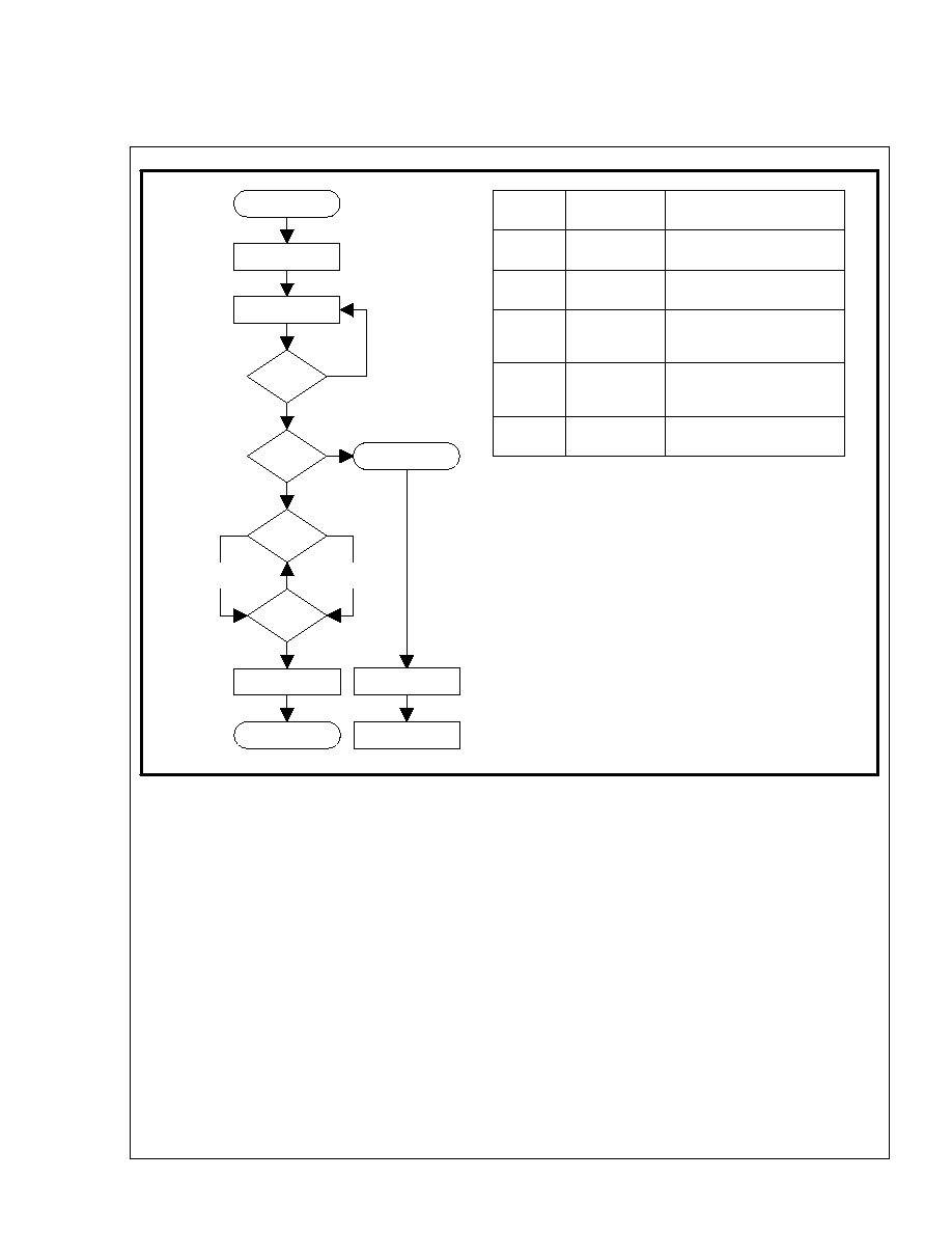
Figure 5. Automated Block Erase Flowchart
sharp
Bus
Operation
Command
Comments
Write
Write
Read
Standby
Setup Byte Write
Byte Write
Data=40H
Addr=Location to Be Written
Data=Data to Be Written
Addr=Location to Be Written
Status Register Data
Check SR.7
1=WSM Ready
0=WSM Busy
Repeat for subsequent byte writes.
SR full status check can be done after each byte write, or after a sequence of
byte writes.
Write FFH after the last byte write operation to place device in
read array mode.
Bus
Operation
Command
Comments
1=V
PP
Error Detect
1=Device Protect Detect
SR.4,SR.3 and SR.1 are only cleared by the Clear Status Register
command in cases where multiple locations are written before
full status is checked.
If error is detected, clear the Status Register before attempting
retry or other error recovery.
Check SR.4
1=Data Write Error
Standby
Standby
Standby
Check SR.3
Check SR.1
RP#=V
IH
,Block Lock-Bit is Set
Only required for systems
implementing lock-bit configuration
Start
Write 40H,
Address
Write Byte
Data and Address
Read
Status Register
SR.7=
0
1
Suspend
Byte Write
No
Yes
Suspend Byte
Write Loop
Full Status
Check if Desired
Byte Write
Complete
FULL STATUS CHECK PROCEDURE
Read Status Register
Data(See Above)
SR.3=
1
0
V
PP
Range Error
Device Protect Error
Byte Write Error
SR.1=
1
0
SR.4=
1
0
Byte Write Successful
LHF08CH1
18
Rev. 1.3
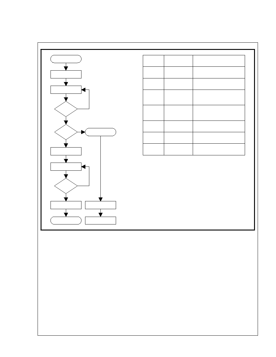
Figure 6. Automated Byte Write Flowchart
sharp
Start
Write B0H
Byte Write Loop
Read
Status Register
SR.7=
0
1
No
Bus
Operation
Command
Comments
Write
Read
Standby
Data=B0H
Addr=X
Data=D0H
Status Register Data
Check SR.7
1=WSM Ready
0=WSM Busy
Yes
SR.6=
0
1
Read Array Data
Done?
Block Erase Resumed
Read Array Data
Block Erase Completed
Write FFH
Write D0H
Standby
Write
Erase
Suspend
Erase
Resume
Addr=X
Addr=X
Check SR.6
1=Block Erase Suspended
0=Block Erase Completed
Read or
Byte Write ?
Read
Byte Write
LHF08CH1
19
Rev. 1.3
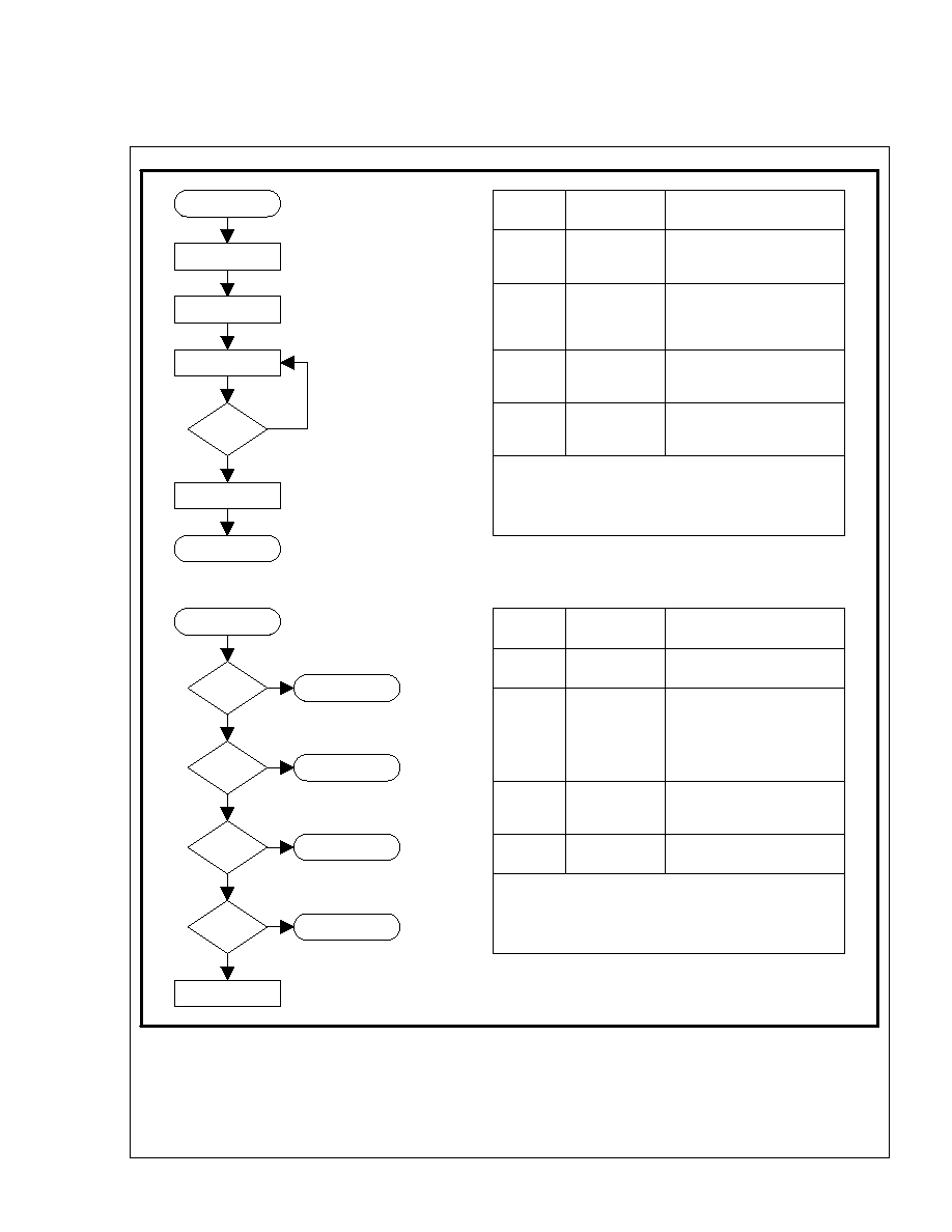
Figure 7. Block Erase Suspend/Resume Flowchart
sharp
Start
Write B0H
Write FFH
Read
Status Register
SR.7=
0
1
No
Bus
Operation
Command
Comments
Write
Read
Standby
Data=B0H
Addr=X
Data=D0H
Status Register Data
Check SR.7
1=WSM Ready
0=WSM Busy
Yes
SR.2=
0
1
Read Array Data
Done
Reading
Byte Write Resumed
Read Array Data
Byte Write Completed
Write FFH
Write D0H
Standby
Write
Write
Read
Byte Write
Suspend
Read Array
Byte Write
Resume
Addr=X
Addr=X
Data=FFH
Addr=X
Check SR.2
1=Byte Write Suspended
0=Byte Write Completed
Read Array locations other
than that being written.
LHF08CH1
20
Rev. 1.3
Figure 8. Byte Write Suspend/Resume Flowchart
sharp
Start
Write 60H,
Block/Device Address
Write 01H/F1H,
Block/Device Address
Read
Status Register
SR.7=
0
1
Full Status
Check if Desired
Complete
Set Lock-Bit
FULL STATUS CHECK PROCEDURE
Read Status Register
Data(See Above)
SR.3=
1
0
V
PP
Range Error
Device Protect Error
Command Sequence
Error
Set Lock-Bit Error
SR.1=
1
0
SR.4,5=
SR.4=
1
1
0
0
Set Lock-Bit Successful
Bus
Operation
Command
Comments
Write
Write
Read
Standby
Data=60H
Addr=Block Address(Block),
Data=01H(Block),
Addr=Block Address(Block),
Status Register Data
Check SR.7
1=WSM Ready
0=WSM Busy
Repeat for subsequent lock-bit set operations.
Full status check can be done after each lock-bit set operation
or after a sequence of lock-bit set operations.
Write FFH after the last lock-bit set operation to place device in
read array mode.
Block/Master
Set
Lock-Bit Setup
Block or Master
Set
Lock-Bit Confirm
Device Address(Master)
F1H(Master)
Device Address(Master)
Bus
Operation
Command
Comments
Standby
1=V
PP
Error Detect
1=Device Protect Detect
Check SR.4,5
Sequence Error
SR.5,SR.4,SR.3 and SR.1 are only cleared by the Clear Status
Register command in cases where multiple lock-bits are set before
full status is checked.
If error is detected, clear the Status Register before attempting
retry or other error recovery.
Check SR.4
1=Set Lock-Bit Error
Standby
Standby
Standby
Check SR.3
Check SR.1
RP#=V
IH
Both 1=Command
(Set Master Lock-BIt Operation)
RP#=V
IH
, Master Lock-Bit is Set
(Set Block Lock-BIt Operation)
LHF08CH1
21
Rev. 1.3
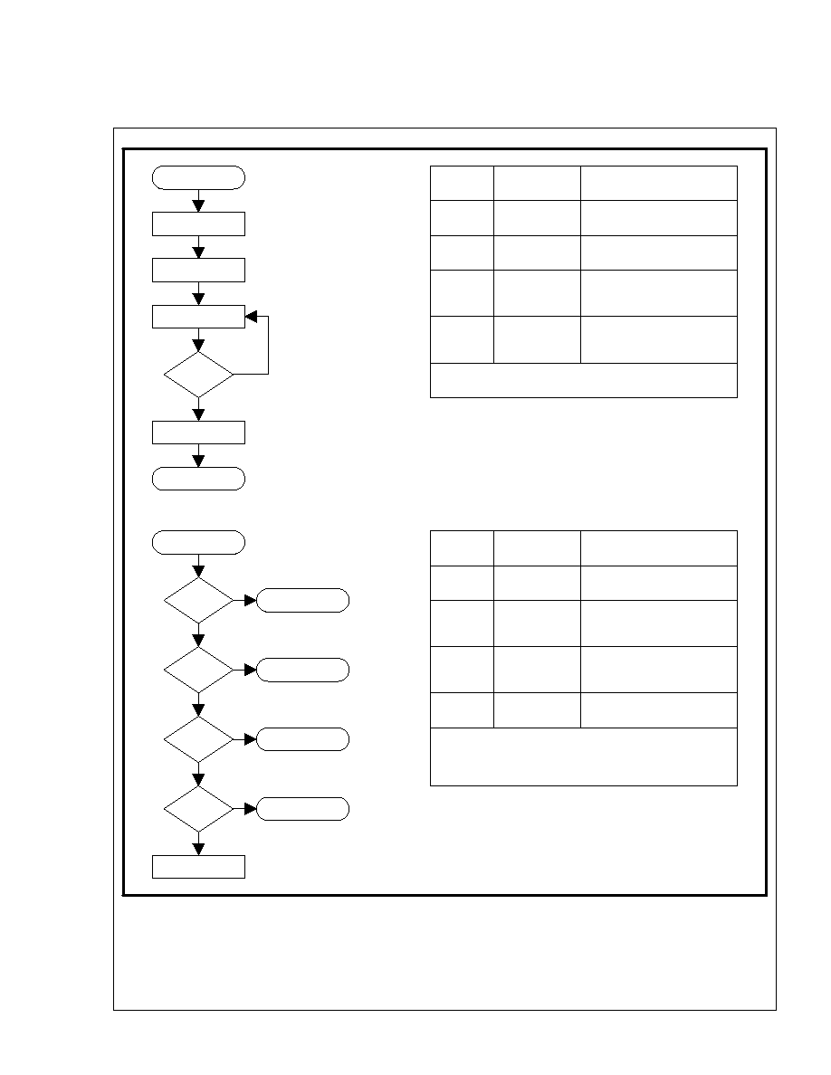
Figure 9. Set Block and Master Lock-Bit Flowchart
sharp
Start
Write 60H
Write D0H
Read
Status Register
SR.7=
0
1
Full Status
Check if Desired
Complete
Clear Block Lock-Bits
FULL STATUS CHECK PROCEDURE
Read Status Register
Data(See Above)
SR.3=
1
0
V
PP
Range Error
Device Protect Error
Command Sequence
Error
Clear Block Lock-Bits
SR.1=
1
0
SR.4,5=
SR.5=
1
1
0
0
Clear Block Lock-Bits
Error
Successful
Bus
Operation
Command
Comments
Write
Write
Read
Standby
Data=60H
Addr=X
Data=D0H
Addr=X
Status Register Data
Check SR.7
1=WSM Ready
0=WSM Busy
Write FFH after the Clear Block Lock-Bits operation to
place device in read array mode.
Clear Block
Lock-Bits Setup
Clear Block
Lock-Bits Confirm
Bus
Operation
Command
Comments
Standby
1=V
PP
Error Detect
1=Device Protect Detect
Check SR.4,5
Sequence Error
SR.5,SR.4,SR.3 and SR.1 are only cleared by the Clear Status
Register command.
If error is detected, clear the Status Register before attempting
retry or other error recovery.
Check SR.5
1=Clear Block Lock-Bits Error
Standby
Standby
Standby
Check SR.3
Check SR.1
Both 1=Command
RP#=V
IH
, Master Lock-Bit is Set
LHF08CH1
22
Rev. 1.3
Figure 10. Clear Block Lock-Bits Flowchart
sharp

LHF08CH1
23
Rev. 1.3
5 DESIGN CONSIDERATIONS
5.1 Three-Line Output Control
The device will often be used in large memory arrays.
SHARP provides three control inputs to
accommodate multiple memory connections.
Three-line control provides for:
a. Lowest possible memory power dissipation.
b. Complete assurance that data bus contention will
not occur.
To use these control inputs efficiently, an address
decoder should enable CE# while OE# should be
connected to all memory devices and the system's
READ# control line. This assures that only selected
memory devices have active outputs while
deselected memory devices are in standby mode.
RP# should be connected to the system
POWERGOOD signal to prevent unintended writes
during system power transitions. POWERGOOD
should also toggle during system reset.
5.2 RY/BY# and Block Erase, Byte Write,
and Lock-Bit Configuration Polling
RY/BY# is a full CMOS output that provides a
hardware method of detecting block erase, byte write
and lock-bit configuration completion. It transitions
low after block erase, byte write, or lock-bit
configuration commands and returns to V
OH
when
the WSM has finished executing the internal
algorithm.
RY/BY# can be connected to an interrupt input of the
system CPU or controller. It is active at all times.
RY/BY# is also V
OH
when the device is in block erase
suspend (with byte write inactive), byte write suspend
or deep power-down modes.
5.3 Power Supply Decoupling
Flash memory power switching characteristics require
careful device decoupling. System designers are
interested in three supply current issues; standby
current levels, active current levels and transient
peaks produced by falling and rising edges of CE#
and OE#. Transient current magnitudes depend on
the device outputs' capacitive and inductive loading.
Two-line control and proper decoupling capacitor
selection will suppress transient voltage peaks. Each
device should have a 0.1µF ceramic capacitor
connected between its V
CC
and GND and between its
V
PP
and GND. These high-frequency, low inductance
capacitors should be placed as close as possible to
package leads. Additionally, for every eight devices,
a 4.7µF electrolytic capacitor should be placed at the
array's power supply connection between V
CC
and
GND. The bulk capacitor will overcome voltage
slumps caused by PC board trace inductance.
5.4 V
PP
Trace on Printed Circuit Boards
Updating flash memories that reside in the target
system requires that the printed circuit board
designer pay attention to the V
PP
Power supply trace.
The V
PP
pin supplies the memory cell current for byte
writing and block erasing. Use similar trace widths
and layout considerations given to the V
CC
power
bus. Adequate V
PP
supply traces and decoupling will
decrease V
PP
voltage spikes and overshoots.
sharp

LHF08CH1
24
Rev. 1.3
5.5 V
CC
, V
PP
, RP# Transitions
Block erase, byte write and lock-bit configuration are
not guaranteed if V
PP
falls outside of a valid V
PPH1/2/3
range, V
CC
falls outside of a valid V
CC2/3/4
range, or
RP#
V
IH
or V
HH
. If V
PP
error is detected, status
register bit SR.3 is set to "1" along with SR.4 or SR.5,
depending on the attempted operation. If RP#
transitions to V
IL
during block erase, byte write, or
lock-bit configuration, RY/BY# will remain low until
the reset operation is complete. Then, the operation
will abort and the device will enter deep power-down.
The aborted operation may leave data partially
altered. Therefore, the command sequence must be
repeated after normal operation is restored. Device
power-off or RP# transitions to V
IL
clear the status
register.
The CUI latches commands issued by system
software and is not altered by V
PP
or CE# transitions
or WSM actions. Its state is read array mode upon
power-up, after exit from deep power-down or after
V
CC
transitions below V
LKO
.
After block erase, byte write, or lock-bit configuration,
even after V
PP
transitions down to V
PPLK
, the CUI
must be placed in read array mode via the Read
Array command if subsequent access to the memory
array is desired.
5.6 Power-Up/Down Protection
The device is designed to offer protection against
accidental block erasure, byte writing, or lock-bit
configuration during power transitions. Upon
power-up, the device is indifferent as to which power
supply (V
PP
or V
CC
) powers-up first. Internal circuitry
resets the CUI to read array mode at power-up.
A system designer must guard against spurious
writes for V
CC
voltages above V
LKO
when V
PP
is
active. Since both WE# and CE# must be low for a
command write, driving either to V
IH
will inhibit writes.
The CUI's two-step command sequence architecture
provides added level of protection against data
alteration.
In-system block lock and unlock capability prevents
inadvertent data alteration. The device is disabled
while RP#=V
IL
regardless of its control inputs state.
5.7 Power Dissipation
When designing portable systems, designers must
consider battery power consumption not only during
device operation, but also for data retention during
system idle time. Flash memory's nonvolatility
increases usable battery life because data is retained
when system power is removed.
In addition, deep power-down mode ensures
extremely low power consumption even when system
power is applied. For example, portable computing
products and other power sensitive applications that
use an array of devices for solid-state storage can
consume negligible power by lowering RP# to V
IL
standby or sleep modes. If access is again needed,
the devices can be read following the t
PHQV
and
t
PHWL
wake-up cycles required after RP# is first
raised to V
IH
. See AC Characteristics- Read Only
and Write Operations and Figures 15, 16 and 17 for
more information.
sharp
LHF08CH1
25
Rev. 1.3
6 ELECTRICAL SPECIFICATIONS
6.1 Absolute Maximum Ratings*
Operating Temperature
During Read, Block Erase, Byte Write
and Lock-Bit Configuration ...........0∞C to +70∞C
(1)
Temperature under Bias............... -10∞C to +80∞C
Storage Temperature........................ -65∞C to +125∞C
Voltage On Any Pin
(except V
CC
, V
PP
, and RP#).......-2.0V to +7.0V
(2)
V
CC
Supply Voltage ..........................-2.0V to +7.0V
(2)
V
PP
Update Voltage during
Block Erase, Byte Write and
Lock-Bit Configuration ........... -2.0V to +14.0V
(2,3)
RP# Voltage with Respect to
GND during Lock-Bit
Configuration Operations ...... -2.0V to +14.0V
(2,3)
Output Short Circuit Current ........................ 100mA
(4)
*WARNING: Stressing the device beyond the
"Absolute Maximum Ratings" may cause permanent
damage. These are stress ratings only. Operation
beyond the "Operating Conditions" is not
recommended and extended exposure beyond the
"Operating Conditions" may affect device reliability.
NOTES:
1. Operating temperature is for commercial
temperature product defined by this specification.
2. All specified voltages are with respect to GND.
Minimum DC voltage is -0.5V on input/output pins
and -0.2V on V
CC
and V
PP
pins. During
transitions, this level may undershoot to -2.0V for
periods <20ns. Maximum DC voltage on
input/output pins and V
CC
is V
CC
+0.5V which,
during transitions, may overshoot to V
CC
+2.0V for
periods <20ns.
3. Maximum DC voltage on V
PP
and RP# may
overshoot to +14.0V for periods <20ns.
4. Output shorted for no more than one second. No
more than one output shorted at a time.
6.2 Operating Conditions
Temperature and V
CC
Operating Conditions
Symbol
Parameter
Notes
Min.
Max.
Unit
Test Condition
T
A
Operating Temperature
0
+70
∞C
Ambient Temperature
V
CC1
V
CC
Supply Voltage (2.7V-3.6V)
1
2.7
3.6
V
V
CC2
V
CC
Supply Voltage (3.3V±0.3V)
3.0
3.6
V
V
CC3
V
CC
Supply Voltage (5V±0.25V)
4.75
5.25
V
V
CC4
V
CC
Supply Voltage (5V±0.5V)
4.50
5.50
V
NOTE:
1. Block erase, byte write and lock-bit configuration operations with V
CC
<3.0V should not be attempted.
6.2.1 CAPACITANCE
(1)
T
A
=+25∞C, f=1MHz
Symbol
Parameter
Typ.
Max.
Unit
Condition
C
IN
Input Capacitance
6
8
pF
V
IN
=0.0V
C
OUT
Output Capacitance
8
12
pF
V
OUT
=0.0V
NOTE:
1. Sampled, not 100% tested.
sharp
AC test inputs are driven at 2.7V for a Logic "1" and 0.0V for a Logic "0." Input timing begins, and output timing ends, at 1.35V.
Input rise and fall times (10% to 90%) <10 ns.
2.7
0.0
INPUT
TEST POINTS
OUTPUT
1.35
1.35
AC test inputs are driven at 3.0V for a Logic "1" and 0.0V for a Logic "0." Input timing begins, and output timing ends, at 1.5V.
Input rise and fall times (10% to 90%) <10 ns.
3.0
0.0
INPUT
TEST POINTS
OUTPUT
1.5
1.5
AC test inputs are driven at V
OH
(2.4 V
TTL
) for a Logic "1" and V
OL
(0.45 V
TTL
) for a Logic "0." Input timing begins at V
IH
(2.0 V
TTL
) and V
IL
(0.8 V
TTL
). Output timing ends at V
IH
and V
IL
. Input rise and fall times (10% to 90%) <10 ns.
2.4
0.45
INPUT
0.8
2.0
TEST POINTS
2.0
0.8
OUTPUT
1.3V
1N914
DEVICE
UNDER
TEST
C
L
OUT
C
L
Includes Jig
R
L
=3.3k
Capacitance
LHF08CH1
26
Rev. 1.3
6.2.2 AC INPUT/OUTPUT TEST CONDITIONS
Figure 11. Transient Input/Output Reference Waveform for V
CC
=2.7V-3.6V
Figure 12. Transient Input/Output Reference Waveform for V
CC
=3.3V±0.3V and V
CC
=5V±0.25V
(High Speed Testing Configuration)
Figure 13. Transient Input/Output Reference Waveform for V
CC
=5V±0.5V
(Standard Testing Configuration)
Test Configuration Capacitance Loading Value
Test Configuration
C
L
(pF)
V
CC
=3.3V±0.3V, 2.7V-3.6V
50
V
CC
=5V±0.25V
30
V
CC
=5V±0.5V
100
Figure 14. Transient Equivalent Testing
Load Circuit
sharp
LHF08CH1
27
Rev. 1.3
6.2.3 DC CHARACTERISTICS
DC Characteristics
V
CC
=2.7V
V
CC
=3.3V
V
CC
=5V
Test
Sym.
Parameter
Notes Typ.
Max.
Typ.
Max.
Typ.
Max.
Unit
Conditions
I
LI
Input Load Current
1
±0.5
±0.5
±1
µA
V
CC
=V
CC
Max.
V
IN
=V
CC
or GND
I
LO
Output Leakage Current
1
±0.5
±0.5
±10
µA
V
CC
=V
CC
Max.
V
OUT
=V
CC
or GND
I
CCS
V
CC
Standby Current
1,3,6
20
100
20
100
25
100
µA
CMOS Inputs
V
CC
=V
CC
Max.
CE#=RP#=V
CC
±0.2V
0.1
2
0.2
2
0.4
2
mA
TTL Inputs
V
CC
=V
CC
Max.
CE#=RP#=V
IH
I
CCD
V
CC
Deep Power-Down
Current
1
10
10
10
µA
RP#=GND±0.2V
I
OUT
(RY/BY#)=0mA
I
CCR
V
CC
Read Current
1,5,6
6
12
7
12
17
35
mA
CMOS Inputs
V
CC
=V
CC
Max.
CE#=GND
f=5MHz(3.3V, 2.7V),
8MHz(5V)
I
OUT
=0mA
7
18
8
18
20
50
mA
TTL Inputs
V
CC
=V
CC
Max.
CE#=GND
f=5MHz(3.3V, 2.7V),
8MHz(5V)
I
OUT
=0mA
I
CCW
V
CC
Byte Write or
1,7
17
mA
V
PP
=3.3V±0.3V
Set Lock-Bit Current
17
35
mA
V
PP
=5.0V±0.5V
12
30
mA
V
PP
=12.0V±0.6V
I
CCE
V
CC
Block Erase or
1,7
17
mA
V
PP
=3.3V±0.3V
Clear Block Lock-Bits
17
30
mA
V
PP
=5.0V±0.5V
Current
12
25
mA
V
PP
=12.0V±0.6V
I
CCWS
I
CCES
V
CC
Byte Write or Block
Erase Suspend Current
1,2
1
6
1
10
mA
CE#=V
IH
I
PPS
V
PP
Standby or Read
1
±2
±15
±2
±15
±2
±15
µA
V
PP
V
CC
I
PPR
Current
10
200
10
200
10
200
µA
V
PP
>V
CC
I
PPD
V
PP
Deep Power-Down
Current
1
0.1
5
0.1
5
0.1
5
µA
RP#=GND±0.2V
I
PPW
V
PP
Byte Write or Set
1,7
40
mA
V
PP
=3.3V±0.3V
Lock-Bit Current
40
40
mA
V
PP
=5.0V±0.5V
15
15
mA
V
PP
=12.0V±0.6V
I
PPE
V
PP
Block Erase or
1,7
20
mA
V
PP
=3.3V±0.3V
Clear Lock-Bit Current
20
20
mA
V
PP
=5.0V±0.5V
15
15
mA
V
PP
=12.0V±0.6V
I
PPWS
I
PPES
V
PP
Byte Write or Block
Erase Suspend Current
1
10
200
10
200
µA
V
PP
=V
PPH1/2/3
sharp
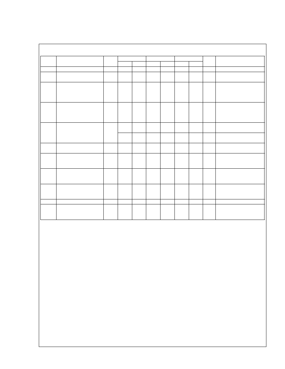
LHF08CH1
28
Rev. 1.3
DC Characteristics (Continued)
V
CC
=2.7V
V
CC
=3.3V
V
CC
=5V
Test
Sym.
Parameter
Notes Min.
Max.
Min.
Max.
Min.
Max.
Unit
Conditions
V
IL
Input Low Voltage
7
-0.5
0.8
-0.5
0.8
-0.5
0.8
V
V
IH
Input High Voltage
7
2.0
V
CC
+0.5
2.0
V
CC
+0.5
2.0
V
CC
+0.5
V
V
OL
Output Low Voltage
3,7
0.4
0.4
0.45
V
V
CC
=V
CC
Min.
I
OL
=5.8mA(V
CC
=5V)
I
OL
=2.0mA
(V
CC
=3.3V, 2.7V)
V
OH1
Output High Voltage
(TTL)
3,7
2.4
2.4
2.4
V
V
CC
=V
CC
Min.
I
OH
=-2.5mA(V
CC
=5V)
I
OH
=-2.0mA(V
CC
=3.3V)
I
OH
=-1.5mA(V
CC
=2.7V)
V
OH2
Output High Voltage
(CMOS)
3,7
0.85
V
CC
0.85
V
CC
0.85
V
CC
V
V
CC
=V
CC
Min.
I
OH
=-2.0mA
V
CC
-0.4
V
CC
-0.4
V
CC
-0.4
V
V
CC
=V
CC
Min.
I
OH
=-100µA
V
PPLK
V
PP
Lockout during
Normal Operations
4,7
1.5
1.5
1.5
V
V
PPH1
V
PP
during Byte Write,
Block Erase or
Lock-Bit Operations
3.0
3.6
V
V
PPH2
V
PP
during Byte Write,
Block Erase or
Lock-Bit Operations
4.5
5.5
4.5
5.5
V
V
PPH3
V
PP
during Byte Write,
Block Erase or
Lock-Bit Operations
11.4
12.6
11.4
12.6
V
V
LKO
V
CC
Lockout Voltage
2.0
2.0
2.0
V
V
HH
RP# Unlock Voltage
8,9
11.4
12.6
11.4
12.6
V
Set master lock-bit
Override master and
block lock-bit
NOTES:
1. All currents are in RMS unless otherwise noted. Typical values at nominal V
CC
voltage and T
A
=+25∞C.
2. I
CCWS
and I
CCES
are specified with the device de-selected. If read or byte written while in erase suspend mode,
the device's current draw is the sum of I
CCWS
or I
CCES
and I
CCR
or I
CCW
, respectively.
3. Includes RY/BY#.
4. Block erases, byte writes, and lock-bit configurations are inhibited when V
PP
V
PPLK
, and not guaranteed in the
range between V
PPLK
(max.) and V
PPH1
(min.), between V
PPH1
(max.) and V
PPH2
(min.), between V
PPH2
(max.)
and V
PPH3
(min.), and above V
PPH3
(max.).
5. Automatic Power Savings (APS) reduces typical I
CCR
to 1mA at 5V V
CC
and 3mA at 2.7V and 3.3V V
CC
in static
operation.
6. CMOS inputs are either V
CC
±0.2V or GND±0.2V. TTL inputs are either V
IL
or V
IH
.
7. Sampled, not 100% tested.
8. Master lock-bit set operations are inhibited when RP#=V
IH
. Block lock-bit configuration operations are inhibited
when the master lock-bit is set and RP#=V
IH
. Block erases and byte writes are inhibited when the corresponding
block-lock bit is set and RP#=V
IH
. Block erase, byte write, and lock-bit configuration operations are not
guaranteed with V
CC
<3.0V or V
IH
<RP#<V
HH
and should not be attempted.
9. RP# connection to a V
HH
supply is allowed for a maximum cumulative period of 80 hours.
sharp
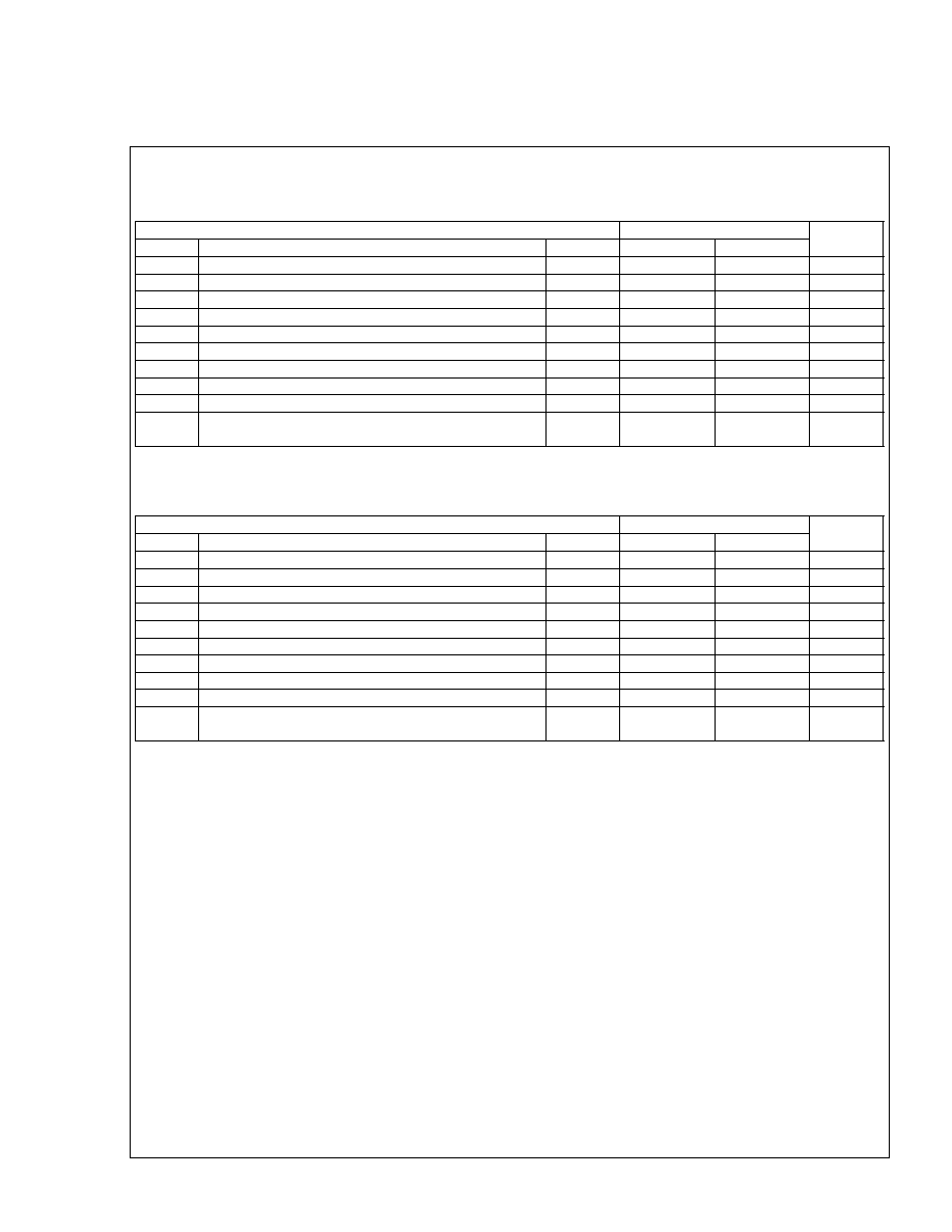
LHF08CH1
29
Rev. 1.3
6.2.4 AC CHARACTERISTICS - READ-ONLY OPERATIONS
(1)
V
CC
=2.7V-3.6V, T
A
=0∞C to +70∞C
Versions
(4)
LH28F008SC-L150
Sym.
Parameter
Notes
Min.
Max.
Unit
t
AVAV
Read Cycle Time
150
ns
t
AVQV
Address to Output Delay
150
ns
t
ELQV
CE# to Output Delay
2
150
ns
t
PHQV
RP# High to Output Delay
600
ns
t
GLQV
OE# to Output Delay
2
50
ns
t
ELQX
CE# to Output in Low Z
3
0
ns
t
EHQZ
CE# High to Output in High Z
3
55
ns
t
GLQX
OE# to Output in Low Z
3
0
ns
t
GHQZ
OE# High to Output in High Z
3
20
ns
t
OH
Output Hold from Address, CE# or OE# Change,
Whichever Occurs First
3
0
ns
NOTE:
See 5.0V V
CC
Read-Only Operations for notes 1 through 4.
V
CC
=3.3V±0.3V, T
A
=0∞C to +70∞C
Versions
(4)
LH28F008SC-L120
Sym.
Parameter
Notes
Min.
Max.
Unit
t
AVAV
Read Cycle Time
120
ns
t
AVQV
Address to Output Delay
120
ns
t
ELQV
CE# to Output Delay
2
120
ns
t
PHQV
RP# High to Output Delay
600
ns
t
GLQV
OE# to Output Delay
2
50
ns
t
ELQX
CE# to Output in Low Z
3
0
ns
t
EHQZ
CE# High to Output in High Z
3
55
ns
t
GLQX
OE# to Output in Low Z
3
0
ns
t
GHQZ
OE# High to Output in High Z
3
20
ns
t
OH
Output Hold from Address, CE# or OE# Change,
Whichever Occurs First
3
0
ns
NOTE:
See 5.0V V
CC
Read-Only Operations for notes 1 through 4.
sharp
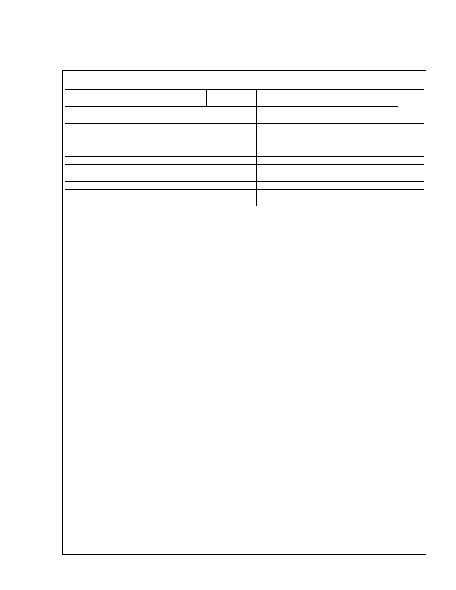
LHF08CH1
30
Rev. 1.3
V
CC
=5V±0.5V, 5V±0.25V, T
A
=0∞C to +70∞C
V
CC
=5V±0.25V LH28F008SC-L85
(5)
Versions
(4)
V
CC
=5V±0.5V
LH28F008SC-L90
(6)
Sym.
Parameter
Notes
Min.
Max.
Min.
Max.
Unit
t
AVAV
Read Cycle Time
85
90
ns
t
AVQV
Address to Output Delay
85
90
ns
t
ELQV
CE# to Output Delay
2
85
90
ns
t
PHQV
RP# High to Output Delay
400
400
ns
t
GLQV
OE# to Output Delay
2
40
45
ns
t
ELQX
CE# to Output in Low Z
3
0
0
ns
t
EHQZ
CE# High to Output in High Z
3
55
55
ns
t
GLQX
OE# to Output in Low Z
3
0
0
ns
t
GHQZ
OE# High to Output in High Z
3
10
10
ns
t
OH
Output Hold from Address, CE# or OE#
Change, Whichever Occurs First
3
0
0
ns
NOTES:
1. See AC Input/Output Reference Waveform for maximum allowable input slew rate.
2. OE# may be delayed up to t
ELQV
-t
GLQV
after the falling edge of CE# without impact on t
ELQV
.
3. Sampled, not 100% tested.
4. See Ordering Information for device speeds (valid operational combinations).
5. See Transient Input/Output Reference Waveform and Transient Equivalent Testing Load Circuit (High Speed
Configuration) for testing characteristics.
6. See Transient Input/Output Reference Waveform and Transient Equivalent Testing Load Circuit (Standard
Configuration) for testing characteristics.
sharp
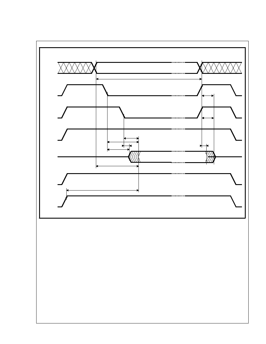
ADDRESSES(A)
CE#(E)
OE#(G)
WE#(W)
DATA(D/Q)
RP#(P)
V
CC
Standby
Device
Address Selection
Data Valid
Address Stable
t
AVAV
t
EHQZ
t
GHQZ
HIGH Z
Valid Output
t
GLQV
t
ELQV
t
GLQX
t
ELQX
t
AVQV
t
PHQV
HIGH Z
t
OH
V
IL
V
OH
V
OL
V
IH
V
IH
V
IH
V
IH
V
IH
V
IL
V
IL
V
IL
V
IL
(DQ
0
-DQ
7
)
LHF08CH1
31
Rev. 1.3
Figure 15. AC Waveform for Read Operations
sharp
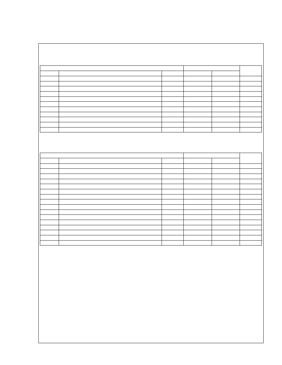
LHF08CH1
32
Rev. 1.3
6.2.5 AC CHARACTERISTICS - WRITE OPERATION
(1)
V
CC
=2.7V-3.6V, T
A
=0∞C to +70∞C
Versions
(5)
LH28F008SC-L150
Sym.
Parameter
Notes
Min.
Max.
Unit
t
AVAV
Write Cycle Time
150
ns
t
PHWL
RP# High Recovery to WE# Going Low
2
1
µs
t
ELWL
CE# Setup to WE# Going Low
0
ns
t
WLWH
WE# Pulse Width
70
ns
t
AVWH
Address Setup to WE# Going High
3
50
ns
t
DVWH
Data Setup to WE# Going High
3
50
ns
t
WHDX
Data Hold from WE# High
5
ns
t
WHAX
Address Hold from WE# High
5
ns
t
WHEH
CE# Hold from WE# High
0
ns
t
WHWL
WE# Pulse Width High
25
ns
t
WHGL
Write Recovery before Read
0
ns
NOTE:
See 5.0V V
CC
WE#-Controlled Writes for notes 1 through 5.
V
CC
=3.3V±0.3V, T
A
=0∞C to +70∞C
Versions
(5)
LH28F008SC-L120
Sym.
Parameter
Notes
Min.
Max.
Unit
t
AVAV
Write Cycle Time
120
ns
t
PHWL
RP# High Recovery to WE# Going Low
2
1
µs
t
ELWL
CE# Setup to WE# Going Low
0
ns
t
WLWH
WE# Pulse Width
70
ns
t
PHHWH
RP# V
HH
Setup to WE# Going High
2
100
ns
t
VPWH
V
PP
Setup to WE# Going High
2
100
ns
t
AVWH
Address Setup to WE# Going High
3
50
ns
t
DVWH
Data Setup to WE# Going High
3
50
ns
t
WHDX
Data Hold from WE# High
5
ns
t
WHAX
Address Hold from WE# High
5
ns
t
WHEH
CE# Hold from WE# High
0
ns
t
WHWL
WE# Pulse Width High
25
ns
t
WHRL
WE# High to RY/BY# Going Low
100
ns
t
WHGL
Write Recovery before Read
0
ns
t
QVVL
V
PP
Hold from Valid SRD, RY/BY# High
2,4
0
ns
t
QVPH
RP# V
HH
Hold from Valid SRD, RY/BY# High
2,4
0
ns
NOTE:
See 5V V
CC
AC Characteristics - Write Operations for Notes 1 through 5.
sharp

LHF08CH1
33
Rev. 1.3
V
CC
=5V±0.5V, 5V±0.25V, T
A
=0∞C to +70∞C
V
CC
=5V±0.25V LH28F008SC-L85
(6)
Versions
(5)
V
CC
=5V±0.5V
LH28F008SC-L90
(7)
Sym.
Parameter
Notes
Min.
Max.
Min.
Max.
Unit
t
AVAV
Write Cycle Time
85
90
ns
t
PHWL
RP# High Recovery to WE# Going Low
2
1
1
µs
t
ELWL
CE# Setup to WE# Going Low
0
0
ns
t
WLWH
WE# Pulse Width
50
50
ns
t
PHHWH
RP# V
HH
Setup to WE# Going High
2
100
100
ns
t
VPWH
V
PP
Setup to WE# Going High
2
100
100
ns
t
AVWH
Address Setup to WE# Going High
3
40
40
ns
t
DVWH
Data Setup to WE# Going High
3
40
40
ns
t
WHDX
Data Hold from WE# High
5
5
ns
t
WHAX
Address Hold from WE# High
5
5
ns
t
WHEH
CE# Hold from WE# High
0
0
ns
t
WHWL
WE# Pulse Width High
25
25
ns
t
WHRL
WE# High to RY/BY# Going Low
90
90
ns
t
WHGL
Write Recovery before Read
0
0
ns
t
QVVL
V
PP
Hold from Valid SRD, RY/BY# High
2,4
0
0
ns
t
QVPH
RP# V
HH
Hold from Valid SRD, RY/BY#
High
2,4
0
0
ns
NOTES:
1. Read timing characteristics during block erase, byte write and lock-bit configuration operations are the same as
during read-onry operations. Refer to AC Characteristics for read-only operations.
2. Sampled, not 100% tested.
3. Refer to Table 4 for valid A
IN
and D
IN
for block erase, byte write, or lock-bit configuration.
4. V
PP
should be held at V
PPH1/2/3
(and if necessary RP# should be held at V
HH
) until determination of block erase,
byte write, or lock-bit configuration success (SR.1/3/4/5=0).
5. See Ordering Information for device speeds (valid operational combinations).
6. See Transient Input/Output Reference Waveform and Transient Equivalent Testing Load Circuit (High Seed
Configuration) for testing characteristics.
7. See Transient Input/Output Reference Waveform and Transient Equivalent Testing Load Circuit (Standard
Configuration) for testing characteristics.
sharp

V
IL
V
IH
V
OH
V
IH
V
IH
V
IH
V
IL
V
IL
V
IL
V
OL
V
IL
V
IH
V
HH
V
IL
V
PPLK
V
PPH3,2,1
V
IH
V
IL
NOTES:
1. V
CC
power-up and standby.
2. Write block erase or byte write setup.
3. Write block erase confirm or valid address and data.
4. Automated erase or program delay.
5. Read status register data.
6. Write Read Array command.
ADDRESSES(A)
CE#(E)
OE#(G)
WE#(W)
DATA(D/Q)
RP#(P)
V
PP
(V)
RY/BY#(R)
}
}
}
}
}
}
1
2
3
4
5
6
A
IN
A
IN
t
AVAV
t
AVWH
t
WHAX
t
ELWL
t
WHEH
t
WHGL
t
WHWL
t
WHQV1,2,3,4
t
WLWH
t
DVWH
t
WHDX
Valid
SRD
t
PHWL
t
WHRL
t
PHHWH
t
QVPH
t
VPWH
t
QVVL
D
IN
D
IN
High Z
D
IN
LHF08CH1
34
Rev. 1.3
Figure 16. AC Waveform for WE#-Controlled Write Operations
sharp

LHF08CH1
35
Rev. 1.3
6.2.6 ALTERNATIVE CE#-CONTROLLED WRITES
(1)
V
CC
=2.7V-3.6V, T
A
=0∞C to +70∞C
Versions
(5)
LH28F008SC-L150
Sym.
Parameter
Notes
Min.
Max.
Unit
t
AVAV
Write Cycle Time
150
ns
t
PHEL
RP# High Recovery to CE# Going Low
2
1
µs
t
WLEL
WE# Setup to CE# Going Low
0
ns
t
ELEH
CE# Pulse Width
70
ns
t
AVEH
Address Setup to CE# Going High
3
50
ns
t
DVEH
Data Setup to CE# Going High
3
50
ns
t
EHDX
Data Hold from CE# High
5
ns
t
EHAX
Address Hold from CE# High
5
ns
t
EHWH
WE# Hold from CE# High
0
ns
t
EHEL
CE# Pulse Width High
25
ns
t
EHGL
Write Recovery before Read
0
ns
NOTE:
See 5.0V V
CC
Alternative CE#-Controlled Writes for notes 1 through 5.
V
CC
=3.3V±0.3V, T
A
=0∞C to +70∞C
Versions
(5)
LH28F008SC-L120
Sym.
Parameter
Notes
Min.
Max.
Unit
t
AVAV
Write Cycle Time
120
ns
t
PHEL
RP# High Recovery to CE# Going Low
2
1
µs
t
WLEL
WE# Setup to CE# Going Low
0
ns
t
ELEH
CE# Pulse Width
70
ns
t
PHHEH
RP# V
HH
Setup to CE# Going High
2
100
ns
t
VPEH
V
PP
Setup to CE# Going High
2
100
ns
t
AVEH
Address Setup to CE# Going High
3
50
ns
t
DVEH
Data Setup to CE# Going High
3
50
ns
t
EHDX
Data Hold from CE# High
5
ns
t
EHAX
Address Hold from CE# High
5
ns
t
EHWH
WE# Hold from CE# High
0
ns
t
EHEL
CE# Pulse Width High
25
ns
t
EHRL
CE# High to RY/BY# Going Low
100
ns
t
EHGL
Write Recovery before Read
0
ns
t
QVVL
V
PP
Hold from Valid SRD, RY/BY# High
2,4
0
ns
t
QVPH
RP# V
HH
Hold from Valid SRD, RY/BY# High
2,4
0
ns
NOTE:
See 5V V
CC
Alternative CE#-Controlled Writes for Notes 1 through 5.
sharp
LHF08CH1
36
Rev. 1.3
V
CC
=5V±0.5V, 5V±0.25V, T
A
=0∞C to +70∞C
V
CC
=5V±0.25V LH28F008SC-L85
(6)
Versions
(5)
V
CC
=5V±0.5V
LH28F008SC-L90
(7)
Sym.
Parameter
Notes
Min.
Max.
Min.
Max.
Unit
t
AVAV
Write Cycle Time
85
90
ns
t
PHEL
RP# High Recovery to CE# Going Low
2
1
1
µs
t
WLEL
WE# Setup to CE# Going Low
0
0
ns
t
ELEH
CE# Pulse Width
50
50
ns
t
PHHEH
RP# V
HH
Setup to CE# Going High
2
100
100
ns
t
VPEH
V
PP
Setup to CE# Going High
2
100
100
ns
t
AVEH
Address Setup to CE# Going High
3
40
40
ns
t
DVEH
Data Setup to CE# Going High
3
40
40
ns
t
EHDX
Data Hold from CE# High
5
5
ns
t
EHAX
Address Hold from CE# High
5
5
ns
t
EHWH
WE# Hold from CE# High
0
0
ns
t
EHEL
CE# Pulse Width High
25
25
ns
t
EHRL
CE# High to RY/BY# Going Low
90
90
ns
t
EHGL
Write Recovery before Read
0
0
ns
t
QVVL
V
PP
Hold from Valid SRD, RY/BY# High
2,4
0
0
ns
t
QVPH
RP# V
HH
Hold from Valid SRD, RY/BY#
High
2,4
0
0
ns
NOTES:
1. In systems where CE# defines the write pulse width (within a longer WE# timing waveform), all setup, hold, and
inactive WE# times should be measured relative to the CE# waveform.
2. Sampled, not 100% tested.
3. Refer to Table 4 for valid A
IN
and D
IN
for block erase, byte write, or lock-bit configuration.
4. V
PP
should be held at V
PPH1/2/3
(and if necessary RP# should be held at V
HH
) until determination of block erase,
byte write, or lock-bit configuration success (SR.1/3/4/5=0).
5. See Ordering Information for device speeds (valid operational combinations).
6. See Transient Input/Output Reference Waveform and Transient Equivalent Testing Load Circuit (High Seed
Configuration) for testing characteristics.
7. See Transient Input/Output Reference Waveform and Transient Equivalent Testing Load Circuit (Standard
Configuration) for testing characteristics.
sharp
V
IL
V
IH
V
OH
V
IH
V
IH
V
IH
V
IL
V
IL
V
IL
V
OL
V
IL
V
IH
V
HH
V
IL
V
PPLK
V
PPH3,2,1
V
IH
V
IL
NOTES:
1. V
CC
power-up and standby.
2. Write block erase or byte write setup.
3. Write block erase confirm or valid address and data.
4. Automated erase or program delay.
5. Read status register data.
6. Write Read Array command.
ADDRESSES(A)
CE#(E)
OE#(G)
WE#(W)
DATA(D/Q)
RP#(P)
V
PP
(V)
RY/BY#(R)
A
IN
A
IN
t
AVAV
t
AVEH
t
EHAX
t
WLEL
t
EHWH
t
EHGL
t
EHEL
t
EHQV1,2,3,4
t
ELEH
t
DVEH
t
EHDX
Valid
SRD
t
PHEL
t
EHRL
t
PHHEH
t
QVPH
t
VPEH
t
QVVL
D
IN
D
IN
High Z
D
IN
}
}
}
}
}
}
1
2
3
4
5
6
LHF08CH1
37
Rev. 1.3
Figure 17. AC Waveform for CE#-Controlled Write Operations
sharp
RP#(P)
V
IL
t
PLPH
t
PLRH
V
IH
V
OH
V
IH
V
OH
V
OL
V
IL
V
OL
t
PLPH
RY/BY#(R)
RY/BY#(R)
RP#(P)
V
IL
t
235VPH
(C)RP# rising Timing
V
IH
2.7V/3.3V/5V
V
IL
RP#(P)
V
CC
(A)Reset During Read Array Mode
(B)Reset During Block Erase, Byte Write, or Lock-Bit Configuretion
LHF08CH1
38
Rev. 1.3
6.2.7 RESET OPERATIONS
Figure 18. AC Waveform for Reset Operation
Reset AC Specifications
V
CC
=2.7V
V
CC
=3.3V
V
CC
=5V
Sym.
Parameter
Notes
Min.
Max.
Min.
Max.
Min.
Max.
Unit
t
PLPH
RP# Pulse Low Time
(If RP# is tied to V
CC
, this
specification is not applicable)
100
100
100
ns
t
PLRH
RP# Low to Reset during
Block Erase, Byte Write or
Lock-Bit Configuration
1,2
20
12
µs
t
235VPH
V
CC
2.7V to RP# High
V
CC
3.0V to RP# High
V
CC
4.5V to RP# High
3
100
100
100
ns
NOTES:
1. If RP# is asserted while a block erase, byte write, or lock-bit configuration operation is not executing, the reset
will complete within 100ns.
2. A reset time, t
PHQV
, is required from the latter of RY/BY# or RP# going high until outputs are valid.
3. When the device power-up, holding RP# low minimum 100ns is required after V
CC
has been in predefined range
and also has been in stable there.
sharp
LHF08CH1
39
Rev. 1.3
6.2.8 BLOCK ERASE, BYTE WRITE AND LOCK-BIT CONFIGURATION PERFORMANCE
(3,4)
V
CC
=3.3V±0.3V, T
A
=0∞C to +70∞C
V
PP
=3.3V
V
PP
=5V
V
PP
=12V
Sym.
Parameter
Notes
Typ.
(1)
Max.
Typ.
(1)
Max.
Typ.
(1)
Max.
Unit
t
WHQV1
t
EHQV1
Byte Write Time
2
19
300
10
150
7
125
µs
Block Write Time
2
1.2
4
0.7
2
0.5
1.5
s
t
WHQV2
t
EHQV2
Block Erase Time
2
0.8
6
0.4
5
0.3
4
s
t
WHQV3
t
EHQV3
Set Lock-Bit Time
2
21
300
13.3
150
11.6
125
µs
t
WHQV4
t
EHQV4
Clear Block Lock-Bits Time
2
1.8
6
1.2
5
1.1
4
s
t
WHRH1
t
EHRH1
Byte Write Suspend Latency
Time to Read
7.1
10
6.6
9.3
7.4
10.4
µs
t
WHRH2
t
EHRH2
Erase Suspend Latency
Time to Read
15.2
21.1
12.3
17.2
12.3
17.2
µs
V
CC
=5V±0.5V, 5V±0.25V, T
A
=0∞C to +70∞C
V
PP
=5V
V
PP
=12V
Sym.
Parameter
Notes
Typ.
(1)
Max.
Typ.
(1)
Max.
Unit
t
WHQV1
t
EHQV1
Byte Write Time
2
8
150
6
100
µs
Block Write Time
2
0.5
1.5
0.4
1
s
t
WHQV2
t
EHQV2
Block Erase Time
2
0.4
5
0.3
4
s
t
WHQV3
t
EHQV3
Set Lock-Bit Time
2
12
150
10
100
µs
t
WHQV4
t
EHQV4
Clear Block Lock-Bits Time
2
1.1
5
1
4
s
t
WHRH1
t
EHRH1
Byte Write Suspend Latency Time to
Read
5.6
7
5.2
7.5
µs
t
WHRH2
t
EHRH2
Erase Suspend Latency Time to Read
9.4
13.1
9.8
12.6
µs
NOTES:
1. Typical values measured at T
A
=+25∞C and nominal voltages. Assumes corresponding lock-bits are not set.
Subject to change based on device characterization.
2. Excludes system-level overhead.
3. Sampled but not 100% tested.
4. Block erase, byte write and lock-bit configuration operations with V
CC
<3.0V and/or V
PP
<3.0V are not
guaranteed.
sharp
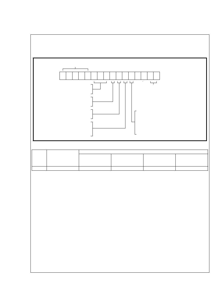
L H 2 8 F 0 0 8 S C
-
H T
Product line designator for all SHARP Flash products
Device Density
008 = 8-Mbit
Power Supply Type
C = SmartVoltage Technology
Architecture
S = Regular Block
Package
T = 40-Lead TSOP
R = 40-Lead TSOP(Reverse Bend)
N = 44-Lead PSOP
Operating Temperature
H = -40∞C ~ +85∞C
Access Speed (ns)
85:85ns(5V,30pF), 90ns(5V),
120ns(3.3V), 150ns(2.7V)
B = 42 or 48-Ball CSP
( )
L
12:120ns(5V), 150ns(3.3V)
Blank = 0∞C ~ +70∞C
170ns(2.7V)
8 5
LHF08CH1
40
Rev. 1.3
7 ADDITIONAL INFORMATION
7.1 Ordering Information
Valid Operational Combinations
Option
Order Code
V
CC
=2.7-3.6V
50pF load,
1.35V I/O Levels
V
CC
=3.3±0.3V
50pF load,
1.5V I/O Levels
V
CC
=5.0±0.5V
100pF load,
TTL I/O Levels
V
CC
=5.0±0.25V
30pF load,
1.5V I/O Levels
1
LH28F008SCT-L85 LH28F008SC-L150 LH28F008SC-L120 LH28F008SC-L90
LH28F008SC-L85
sharp

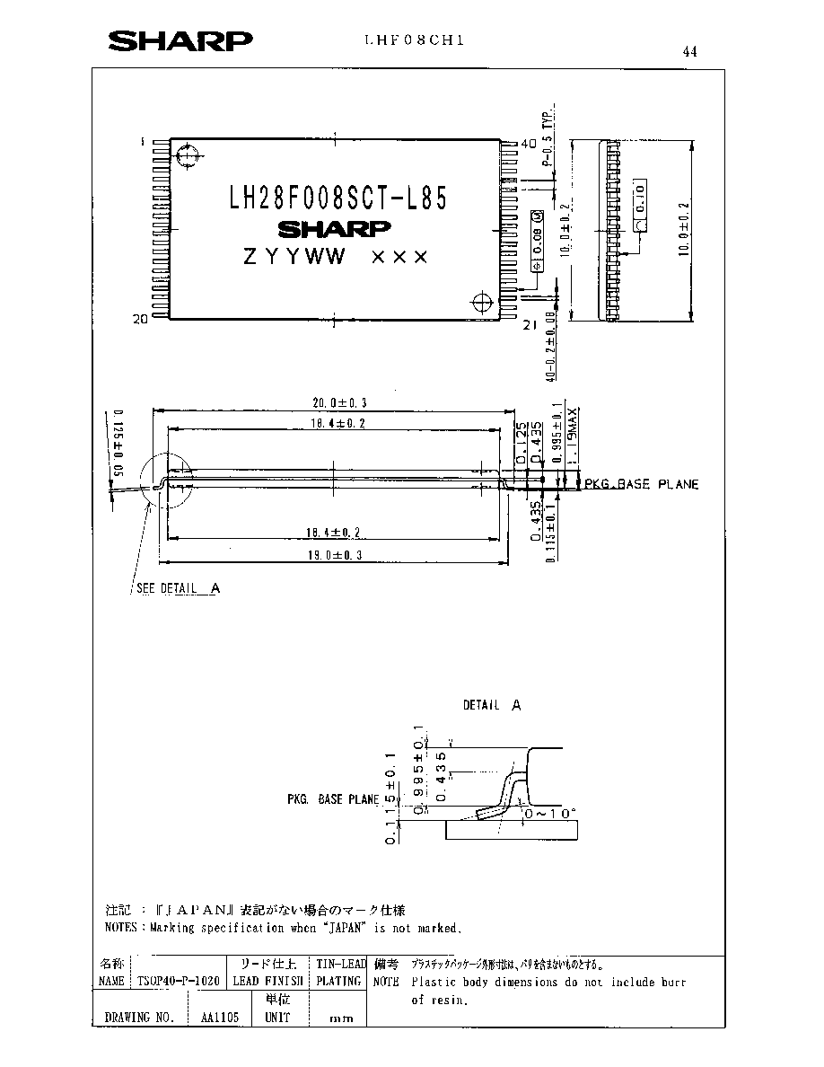
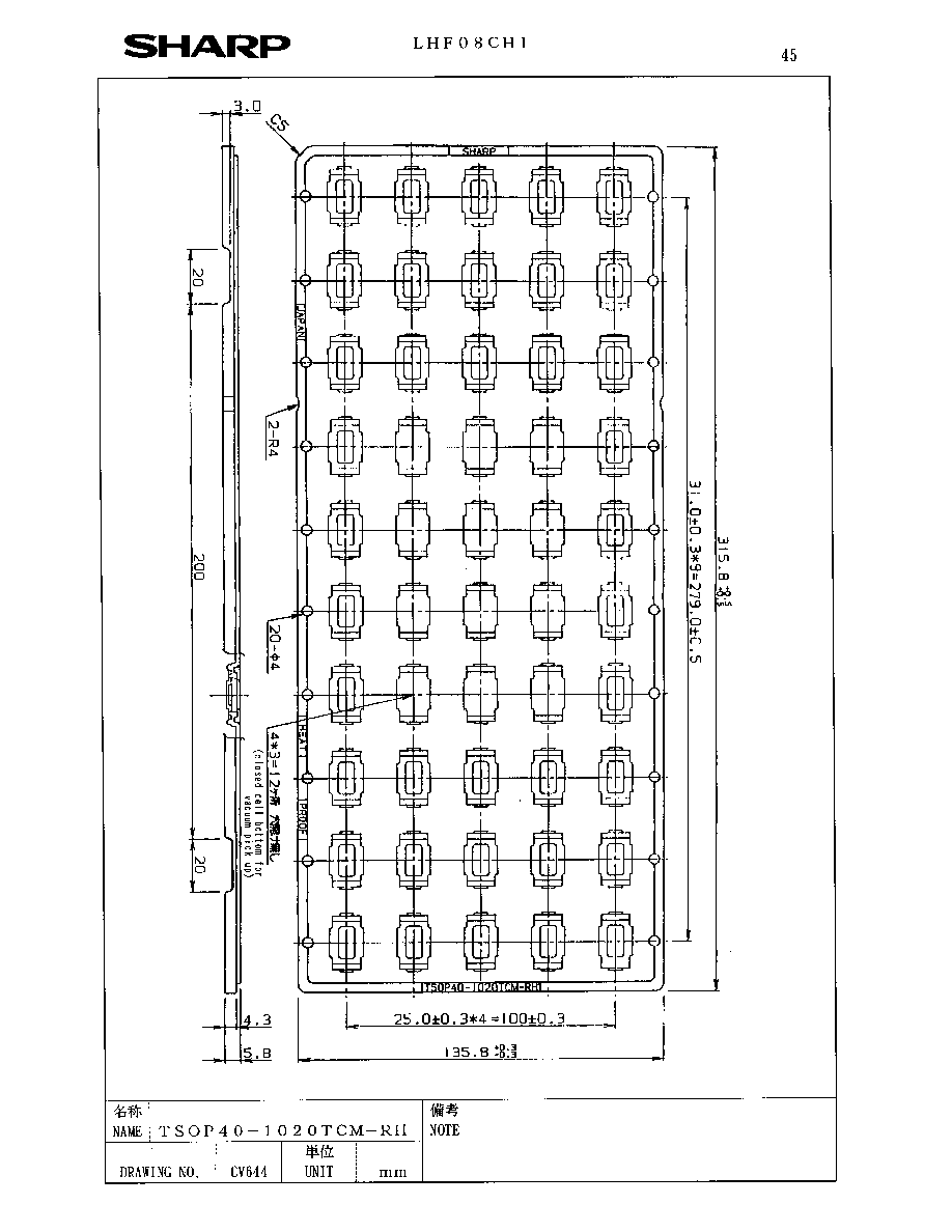
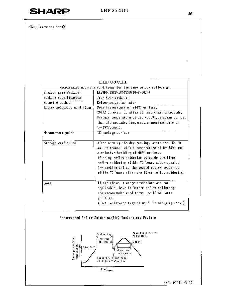
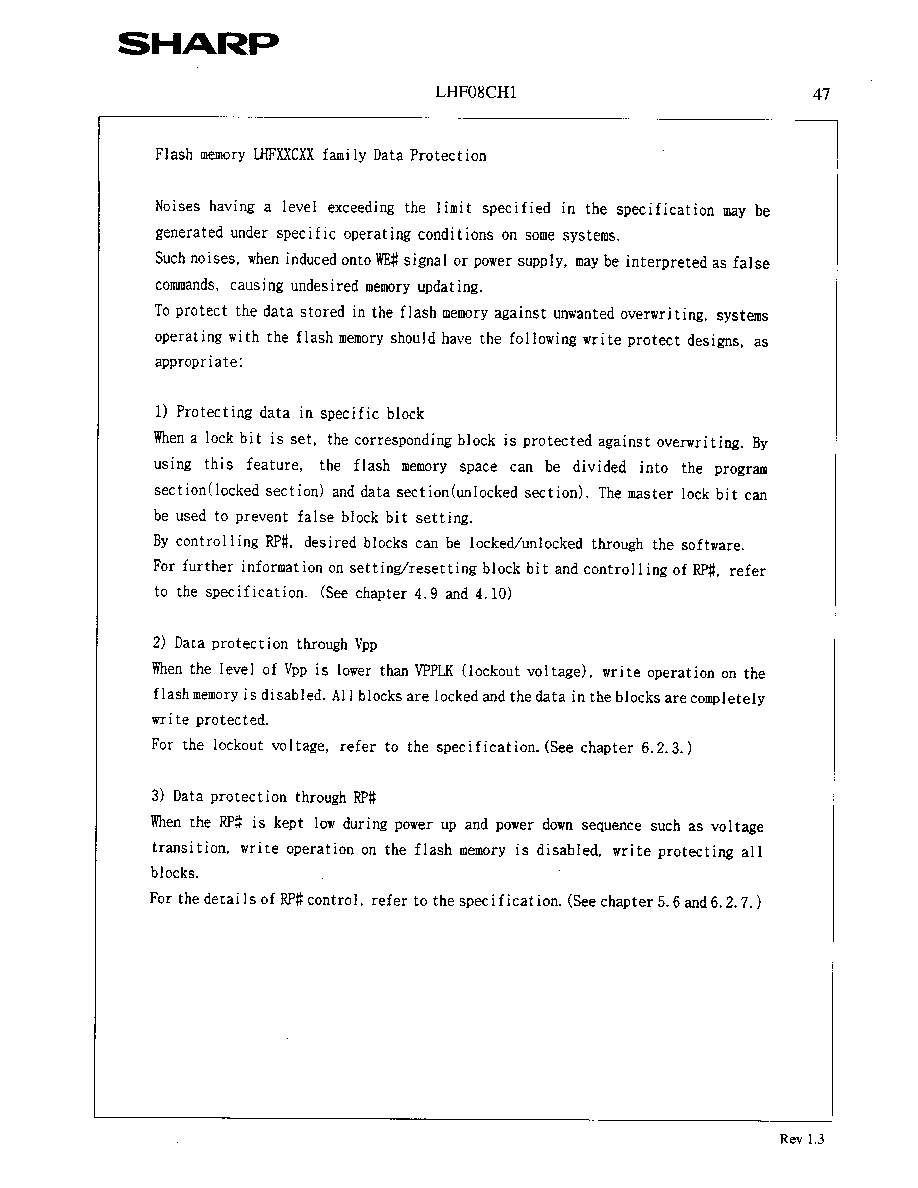

Rev. 1.10
i
A-1 RECOMMENDED OPERATING CONDITIONS
A-1.1 At Device Power-Up
AC timing illustrated in Figure A-1 is recommended for the supply voltages and the control signals at device power-up.
If the timing in the figure is ignored, the device may not operate correctly.
Figure A-1. AC Timing at Device Power-Up
For the AC specifications t
VR
, t
R
, t
F
in the figure, refer to the next page. See the "ELECTRICAL SPECIFICATIONS"
described in specifications for the supply voltage range, the operating temperature and the AC specifications not shown in
the next page.
t
2VPH
*1
V
CC
GND
V
CC
(min)
RP#
V
IL
V
IH
(P)
t
PHQV
V
CCW
*2
GND
V
CCWH1/2
(V)
CE#
V
IL
V
IH
(E)
WE#
V
IL
V
IH
(W)
OE#
V
IL
V
IH
(G)
WP#
V
IL
V
IH
(S)
V
OH
V
OL
(D/Q)
DATA
High Z
Valid
Output
t
VR
t
F
t
R
t
ELQV
t
F
t
GLQV
(A)
ADDRESS
Valid
(RST#)
(V
PP
)
t
R
or
t
F
Address
V
IL
V
IH
t
AVQV
*1 t
5VPH
for the device in 5V operations.
t
R
or
t
F
t
R
t
R
*2 To prevent the unwanted writes, system designers should consider the V
CCW
(V
PP
) switch, which connects V
CCW
(V
PP
)
to GND during read operations and V
CCWH1/2
(V
PPH1/2
) during write or erase operations.
(V
PPH1/2
)
See the application note AP-007-SW-E for details.
sharp
Rev. 1.10
ii
A-1.1.1 Rise and Fall Time
NOTES:
1. Sampled, not 100% tested.
2. This specification is applied for not only the device power-up but also the normal operations.
t
R
(Max.) and t
F
(Max.) for RP# (RST#) are 100
µs/V.
Symbol
Parameter
Notes
Min.
Max.
Unit
t
VR
V
CC
Rise Time
1
0.5
30000
µs/V
t
R
Input Signal Rise Time
1, 2
1
µs/V
t
F
Input Signal Fall Time
1, 2
1
µs/V
sharp
Rev. 1.10
iii
A-1.2 Glitch Noises
Do not input the glitch noises which are below V
IH
(Min.) or above V
IL
(Max.) on address, data, reset, and control signals,
as shown in Figure A-2 (b). The acceptable glitch noises are illustrated in Figure A-2 (a).
Figure A-2. Waveform for Glitch Noises
See the "DC CHARACTERISTICS" described in specifications for V
IH
(Min.) and V
IL
(Max.).
(a) Acceptable Glitch Noises
Input Signal
V
IH
(Min.)
Input Signal
V
IH
(Min.)
Input Signal
V
IL
(Max.)
Input Signal
V
IL
(Max.)
(b)
NOT
Acceptable Glitch Noises
sharp
Rev. 1.10
iv
A-2 RELATED DOCUMENT INFORMATION
(1)
NOTE:
1. International customers should contact their local SHARP or distribution sales office.
Document No.
Document Name
AP-001-SD-E
Flash Memory Family Software Drivers
AP-006-PT-E
Data Protection Method of SHARP Flash Memory
AP-007-SW-E
RP#, V
PP
Electric Potential Switching Circuit
sharp

SPECIFICATIONS ARE SUBJECT TO CHANGE WITHOUT NOTICE.
Suggested applications (if any) are for standard use; See Important Restrictions for limitations on special applications. See Limited
Warranty for SHARP's product warranty. The Limited Warranty is in lieu, and exclusive of, all other warranties, express or implied.
ALL EXPRESS AND IMPLIED WARRANTIES, INCLUDING THE WARRANTIES OF MERCHANTABILITY, FITNESS FOR USE AND
FITNESS FOR A PARTICULAR PURPOSE, ARE SPECIFICALLY EXCLUDED. In no event will SHARP be liable, or in any way responsible,
for any incidental or consequential economic or property damage.
NORTH AMERICA
EUROPE
JAPAN
SHARP Microelectronics of the Americas
5700 NW Pacific Rim Blvd.
Camas, WA 98607, U.S.A.
Phone: (1) 360-834-2500
Fax: (1) 360-834-8903
Fast Info: (1) 800-833-9437
www.sharpsma.com
SHARP Microelectronics Europe
Division of Sharp Electronics (Europe) GmbH
Sonninstrasse 3
20097 Hamburg, Germany
Phone: (49) 40-2376-2286
Fax: (49) 40-2376-2232
www.sharpsme.com
SHARP Corporation
Electronic Components & Devices
22-22 Nagaike-cho, Abeno-Ku
Osaka 545-8522, Japan
Phone: (81) 6-6621-1221
Fax: (81) 6117-725300/6117-725301
www.sharp-world.com
TAIWAN
SINGAPORE
KOREA
SHARP Electronic Components
(Taiwan) Corporation
8F-A, No. 16, Sec. 4, Nanking E. Rd.
Taipei, Taiwan, Republic of China
Phone: (886) 2-2577-7341
Fax: (886) 2-2577-7326/2-2577-7328
SHARP Electronics (Singapore) PTE., Ltd.
438A, Alexandra Road, #05-01/02
Alexandra Technopark,
Singapore 119967
Phone: (65) 271-3566
Fax: (65) 271-3855
SHARP Electronic Components
(Korea) Corporation
RM 501 Geosung B/D, 541
Dohwa-dong, Mapo-ku
Seoul 121-701, Korea
Phone: (82) 2-711-5813 ~ 8
Fax: (82) 2-711-5819
CHINA
HONG KONG
SHARP Microelectronics of China
(Shanghai) Co., Ltd.
28 Xin Jin Qiao Road King Tower 16F
Pudong Shanghai, 201206 P.R. China
Phone: (86) 21-5854-7710/21-5834-6056
Fax: (86) 21-5854-4340/21-5834-6057
Head Office:
No. 360, Bashen Road,
Xin Development Bldg. 22
Waigaoqiao Free Trade Zone Shanghai
200131 P.R. China
Email: smc@china.global.sharp.co.jp
SHARP-ROXY (Hong Kong) Ltd.
3rd Business Division,
17/F, Admiralty Centre, Tower 1
18 Harcourt Road, Hong Kong
Phone: (852) 28229311
Fax: (852) 28660779
www.sharp.com.hk
Shenzhen Representative Office:
Room 13B1, Tower C,
Electronics Science & Technology Building
Shen Nan Zhong Road
Shenzhen, P.R. China
Phone: (86) 755-3273731
Fax: (86) 755-3273735