
LD14702-1
1. Application
This specification applies to color TFT-LCD module, LQ104V1DG21
These specification sheets are the proprietary product of SHARP CORPORATION("SHARP) and include
materials protected under copyright of SHARP. Do not reproduce or cause any third party to reproduce
them in any form or by any means, electronic or mechanical, for any purpose, in whole or in part, without
the express written permission of SHARP .
The device listed in these specification sheets was designed and manufactured for use in general electronic
equipment.
In case of using the device for applications such as control and safety equipment for transportation(aircraft,
trains, automobiles, etc. ), rescue and security equipment and various safety related equipment which
require higher reliability and safety, take into consideration that appropriate measures such as fail-safe
functions and redundant system design should be taken .
Do not use the device for equipment that requires an extreme level of reliability, such as aerospace
applications, telecommunication equipment(trunk lines), nuclear power control equipment and medical or
other equipment for life support .
SHARP assumes no responsibility for any damage resulting from the use of the device which does not
comply with the instructions and the precautions specified in these specification sheets .
Contact and consult with a SHARP sales representative for any questions about this device .
2. Overview
This module is a color active matrix LCD module incorporating amorphous silicon TFT
(Thin Film Transistor). It is composed of a color TFT-LCD panel, driver ICs, control
circuit and power supply circuit and a backlight unit. Graphics and texts can be
displayed on a 640�3�480 dots panel with 262,144 colors by supplying 18 bit data signal
(6bit/color), four timing signals,+3.3V/ +5V DC supply voltage for TFT-LCD panel driving and
supply voltage for backlight.
The TFT-LCD panel used for this module is a low-reflection and higher-color-saturation
type. Therefore, this module is also suitable for the multimedia use.
Optimum viewing direction is 6 o'clock.
Backlight-driving DC/AC inverter is not built in this module.
LD14702-2
3. Mechanical Specifications
Parameter Specifications
Unit
Display size
26 (10.4") Diagonal
cm
Active area
211.2(H)�158.4(V)
mm
Pixel format
640(H)�480(V)
pixel
(1 pixelRGB dots)
Pixel pitch
0.330(H)�0.330(V)
mm
Pixel configuration
R,G,B vertical stripe
Display mode
Normally white
Unit outline dimensions *1 265.0(W)�195.0(H)�11.5max(D)
mm
Mass
700(max)
g
Surface treatment
Anti-glare and hard-coating 3H
*1.Note: excluding backlight cables.
Outline dimensions is shown in Fig.1
LD14702-3
4. Input Terminals
4-1. TFT-LCD panel driving
CN1 Used connector:DF9MA-31P-1V (Hirose Electric Co., Ltd.)
Corresponding connector: DF9-31S-1V ( )
DF9A-31S-1V( )
DF9B-31S-1V( )
DF9M-31S-1V( )
Pin No. Symbol
Function
Remark
1
GND
2
CK
Clock signal for sampling each data signal
3
Hsync Horizontal synchronous signal
Note1
4
Vsync Vertical synchronous signal
Note1
5 GND
6 R0
data signal(LSB
7 R1
data signal
8 R2
data signal
9 R3
data signal
10 R4
data signal
11 R5
data signal(MSB)
12 GND
13 G0
data signal(LSB
14 G1
data signal
15 G2
data signal
16 G3
data signal
17 G4
data signal
18 G5
data signal(MSB)
19 GND
20 B0
data signal(LSB
21 B1
data signal
22 B2
data signal
23 B3
data signal
24 B4
data signal
25 B5
data signal(MSB)
26 GND
27
ENAB Signal to settle the horizontal display position
Note2
28 Vcc
3.3/5.0V power supply
29 Vcc
3.3/5.0V power supply
30
R/L
Horizontal display mode select signal
Note3
31
U/D
Vertical display mode select signal
Note4
The shielding case is connected with GND.
Note1480 line, 400 line or 350 line mode
is selected by the polarity combination
of the both synchronous signals.
Note2The horizontal display start timing is settled in
accordance with a rising timing of ENAB signal. In case ENAB is fixed "Low", the horizontal start timing is
determined as described in 7-2. Don't keep ENAB "High" during operation.
1
2
30
31
CN1 pin arrangement from module surface
(Transparent view)
Mode
480 lines
400 lines
350 lines
Hsync Negative Negative Positive
Vsync Negative Positive Negative
LD14702-4
Note3
Note4
4-2. Backlight driving
Used connector : BHR-03VS-1(JST)
CN2CN3 Corresponding connector :SM02(8.0)B-BHS(JST)
Pin no.
Symbol
Function
1
HIGH
Power supply for lamp
(High voltage side)
2
NC
This is electrically opened.
3
LOW
Power supply for lamp
(Low voltage side)
5. Absolute Maximum Ratings
Parameter Symbol
Condition
Ratings
Unit
Remark
Input voltage
V
I
Ta=25 -0.3 Vcc0.3 Note1
+5V supply voltage
Vcc
Ta=25 0 6
Storage temperature
Tstg
-
-30 70
Note2
Operating temperature (Ambient) Topa
-
-10 65
Note1CK,R0R5,G0G5,B0B5,Hsync,Vsync,ENAB, R/L, U/L
Note2Humidity95%RH Max. at Ta40.
Maximum wet-bulb temperature at 39 or less at Ta>40.
No condensation.
LD14702-5
6. Electrical Characteristics
6-1.TFT-LCDpaneldriving
Ta25
Parameter Symbol
Min.
Typ.
Max.
Unit
Remark
Supply voltage
Vcc
+3.0 +3.3 +5.0 +5.5
V
Note1
Icc
-
(180)
TBD
Vcc=3.3V
Note2
Power
Supply Current dissipation
Icc
-
(150) TBD
Vcc=5.0V
Note2
Permissive input ripple voltage
V
RF
-
-
100 mVp-p
Input voltage (Low)
V
IL
-
-
0.3Vcc
Input voltage (High)
V
IH
0.7Vcc
-
-
Note3
I
OL1
-
-
1.0
V
I
=0V
Note4
Input current (low)
I
OL2
-
-
60.0
V
I
=0V
Note5
Input current (High)
I
OH1
-
-
1.0
V
I
=Vcc
Note6
I
OH2
-
-
60.0
V
I
=Vcc
Note7
NOTE 1
Vcc-turn-on conditions
Vcc-dip conditions
Vcc-dip condition should also follow
The Vcc-turn-on conditions
Note2 Typical current situation : 16-gray-bar pattern.
480 line mode/Vcc=+3.3V/5.0V
Note3 CK,R0~R5,G0~G5,B0~B5,Hsync,Vsync,ENAB,
R/L,U/D
Note4 CK,R0~R5,G0~G5,B0~B5,Hsync,Vsync,ENAB
Note5 R/L
Note6 CK,R0~R5,G0~G5,B0~B5,Hsnc,Vsync
Note7 ENAB,U/D
T
2.8V
0.3V
VCC
T1 T
2.8V
0.3V
VCC
T
3.0V
2.5V
VCC
R G B
G S 0
R G B
G S 3
R G B
G S 7
R G B
G S 5 9
R G B
G S 6 3
. . . .
LD14702-6
6-2. Backlight driving
The backlight system is an edge-lighting type with double CCFT (Cold Cathode
Fluorescent Tube). The characteristics of single lamp are shown in the following table.
Ta=25
Parameter
Symbol Min.
Typ. Max. Unit
Remark
Lamp current
I
L
2.0 6.0 6.5
mArms
Note1
Lamp power consumption
P
L
-
3.0
-
Note2
Lamp frequency
F
L
20 35
60 KHz
Note3
Kick-off voltage
Vs
-
-
(950) Vrms
Ta=25
-
-
(1250) Vrms
Ta =0Note4
-
-
(1500) Vrms
Ta =-10Note4
Lamp life time
L
L
50000
-
-
hour Note5
Note1 Lamp current is measured with current meter for high frequency as shown below.
Note2 At the condition of I
L
=6.0mArms
Note3 Lamp frequency may produce interference with horizontal synchronous frequency,and
this may cause beat on the display. Therefore lamp frequency shall be detached as
much as possible from the horizontal synchronous frequency and from the harmonics
of horizontal synchronous to avoid interference.
Note4The open output voltage of the inverter shall be maintained for more than 1sec; otherwise
the lamp may not be turned on.
Note5Since lamp is consumables, the life time written above is referencial value and it is not
guaranteed in this specification sheet by SHARP.
Lamp life time is defined that it applied either or under this condition
(Continuous turning on at Ta=25, IL=6.0mArms)
Brightness becomes 50% of the original value under standard condition.
Kick-off voltage at Ta=-10 exceeds maximum value,(1500)Vrms.
In case of operating under lower temp environment, the lamp exhaustion is accelerated and the
brightness becomes lower.
(Continuous operating under for around 1 month under lower temp condition may reduce the
brightness to half of the original brightness.)
In case of such usage under lower temp environment, periodical lamp exchange is recommended.
Note6The performance of the backlight, for example life time or brightness, is much influenced
by the characteristics of the DC-AC inverter for the lamp. When you design or order the
inverter, please make sure that a poor lighting caused by the mismatch of the backlight and
the inverter (miss-lighting,flicker, etc.) never occur. when you confirm it, the module should
be operated in the same condition as it is installed in your instrument.
Note7 It is required to have the inverter designed so that to allow the impedance deviation
of the two CCFT lamps and the capacity deviation of barast capacitor.
Module
Inverter
* 3pin is V
LOW
3
3

LD14702-7
7. Timing Characteristics of input signals
Timing diagrams of input signal are shown in Fig.2 - .
7-1. Timing characteristics
Parameter Symbol
Mode
Min.
Typ.
Max.
Unit
Remark
Clock
Frequency
1/Tc all
-
25.18 28.33
MHz
High
time
Tch
5
-
-
ns
Low
time
Tcl
10
-
-
ns
Data
Setup time
Tds
5
-
-
ns
Hold
time
Tdh
10
-
-
ns
Horizontal Cycle
TH
30.00 31.78 -
s
sync. signal
750 800 900
clock
Pulse
width
THp
2 96 200
clock
Vertical
Cycle
TV
480
515
525
560
line
sync.
signal
400 446 449 480 line
350 447 449 510 line
Pulsewidth
TVp
all
1
-
34 line
Horizontal display period
THd
640 640 640
clock
Hsync-Clock
THc
10
-
Tc-10 ns
phase
difference
Hsync-Vsync
TVh
0
-
TH-THp clock
phase difference
Note) In case of lower frequency, the deterioration of display quality, flicker etc.,may be occurred.
7-2. Horizontal display position
The horizontal display position is determined by ENAB signal and the input data corresponding
to the rising edge of ENAB signal is displayed at the left end of the active area.
Parameter symbol
Min.
Typ.
Max.
Unit
Remark
Enable signal Setup time
Tes
5
-
Tc-10 ns
Pulse
width
Tep
2
640
640
clock
Hsync-Enable signal
phase difference
THe 44 -
TH-664 clock
Note) When ENAB is fixed "Low", the display starts from the data of C104(clock) as shown
in Fig.2-. Be careful that the module does not work when ENAB is fixed "High".
When the phase difference is below 104 clock, keep the "High level of ENAB is signal longer
Than 104-The. If it will not be keeped, the display starts from the data of C104(clock).
7-3. Vertical display position
The vertical display position is automatically centered in the active area at each mode
LD14702-8
of VGA ,480-,400-,and 350-line mode . Each mode is selected depending on the polarity of
the synchronous signals described in 4-1(Note1).
In each mode ,the data of TVn is displayed at the top line of the active area. And the
display position will be centered on the screen like the following figure when the period of
vertical synchronous signal,TV,is typical value.
In 400-,and 350-line mode,the data in the vertical data invalid period is also displayed,
So ,inputting all data "0" is recommended during vertical data invalid period.
ENAB signal has no relation to the vertical display position.
Mode V-data
start(TVs)
V-data
period(TVd)
V-display start(TVn) V-display period Unit
Remark
480 34
480
34
480
line
400 34
400
443-TV
480
line
350 61
350
445-TV
480
line
7-4. Input Data Signals and Display Position on the screen
data invalid period
lines
lines
lines
lines
lines
lines
400 lines mode (TV=449)
350 lines mode (TV=449)
data period
data invalid period
data invalid period
data invalid period
data period
D 1 , DH 1
D 1 , DH 2
D 1 , DH 3
D 2 , DH 2
D 2 , DH 1
D 3 , DH 1
D 6 4 0, DH 1
D640,DH480
D 1 , DH 48 0
R G B
D is pl ay po sition of i np ut da ta (480 l in es mo de )
LD14702-9
THc
C1*
C2*
* Only when enable terminal is fixed "Low"
D1
D2
D3
Tds
Tdh
Tch
Tcl
Tc
D639
D640
Horizontal invalid da ta period
THp
C104*
Number of clock
Number of H-data
THe
Tes
THd
Tep
TH
DH1
DH2
DH3
DH479
DH480
Vertical invalid data period
TVh
TVp
TV
TVs
TVd
Number of V-data line
1
2
34
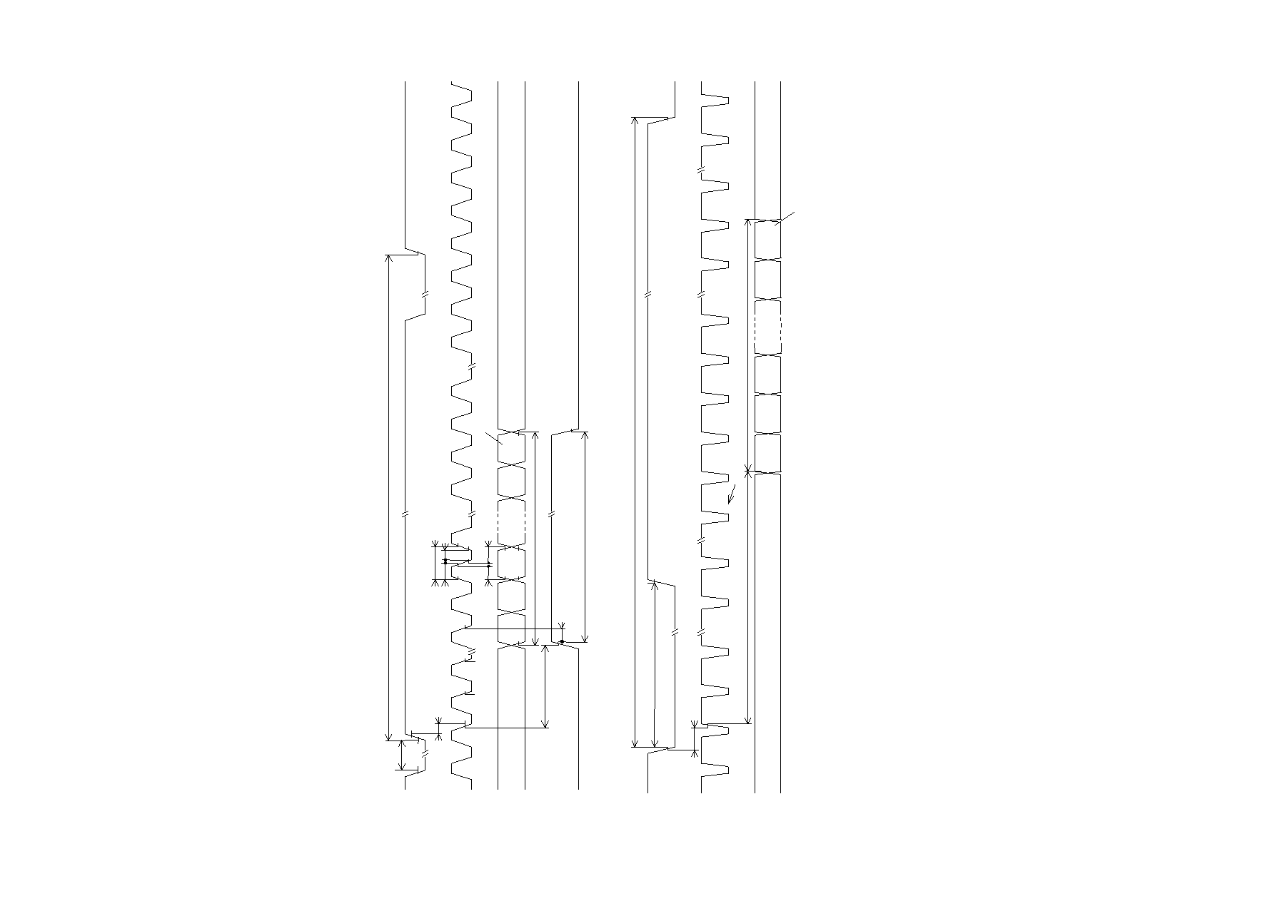
Fig 2-1 Input signal waveforms (480 line mode)
Horizontal
sync. signal
(Hsync)
Clock signal
(CK)
Data signal
(R0~R5,G0~G5,
B0~B5)
Data enable signal
(ENAB)
Vertical
sync. signal
(Vsync)
Horizontal
sync.
signal
(Hsync)
Data signal
(R0~R5,G0~G5,
B0~B5)
Horizontal invalid da ta period
Vertical invalid data period
0.3Vcc
0.3Vcc
0.3Vcc
0.3Vcc
0.7Vcc
0.3Vcc
0.3Vcc
0.7Vcc
0.3Vcc
0.7Vcc
0.3Vcc
0.3Vcc
0.3Vcc
0.7Vcc
0.7Vcc
0.3Vcc
0.3Vcc
0.7Vcc
Number of line
LD14702-10
THc
C1*
C2*
* Only when enable terminal (ENAB) is fixed "Low"
D1
D2
D3
Tds
Tdh
Tch
Tcl
Tc
D639
D640
Horizontal data invalid
period
THp
C104*
Number of H-data
THe
Tes
THd
Tep
TH
DH1
DH2
DH3
DH399
DH400
Vertical invalid data period
TVh
TVp
TV
TVs
TVd
1
2
34
Number of line
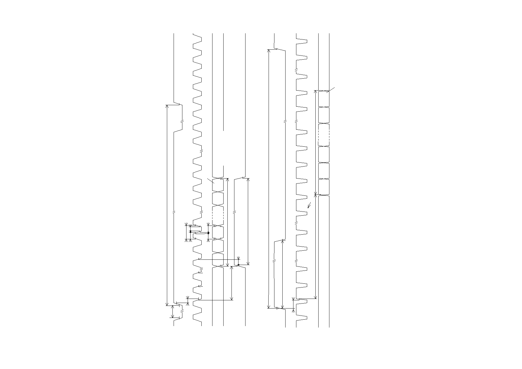
Fig.2-2 Input signal waveforms (400 line mode)
Horizontal
sync.
signal
(Hsync)
Clock signal
(CK)
Data signal
(R0~R5,G0~G5,
B0~B5)
Data enable
signal
(ENAB)
Vertical
sync.
signal
(Vsync)
Horizontal
sync. signal
(Hsync)
Data signal
(R0~R5,G0~G5,
B0~B5)
Horizontal data invalid
period
Vertical invalid data period
0.3Vcc
0.3Vcc
0.3Vcc
0.7Vcc
0.7Vcc
0.3Vcc
0.3Vcc
0.3Vcc
0.7Vcc
0.3Vcc
0.3Vcc
0.3Vcc
0.7Vcc
0.3Vcc
0.7Vcc
0.7Vcc
0.7Vcc
Number of clock
Number of V-data line
LD14702-11
Horizontal
sync. signal
(Hsync)
Clock signal
(CK)
Data signal
(R0~R5,G0~G5,
B0~B5)
THc
C1*
C2*
D1
D2
D3
Tds
Tdh
Tch
Tcl
Tc
D639
D640
Horizontal invalid data period
Data enable signal
(ENAB)
C104*
Number of H-data
THe
Tes
THd
Tep
THp
TH
DH1
DH2
DH3
DH349
DH350
Vertical invalid data period
Vertical
sync. signal
(Vsync)
TVh
TVp
TV
TVs
TVd
Number of V-data line
1
2
Number of
line
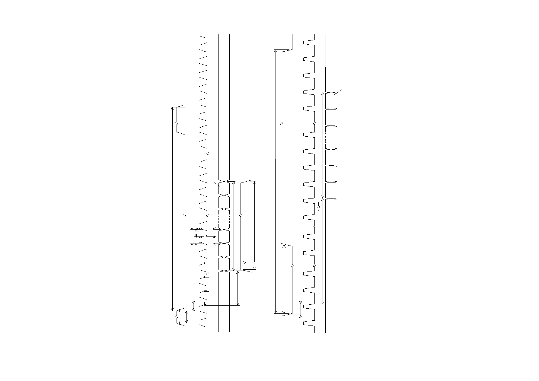
Fig.2-3 Input signal waveforms (350 line mode)
61
Horizontal
sync. signal
(Hsync)
Data signal
(R0~R5,G0~G5,
B0~B5)
* Only when enable terminal (ENAB) fixed to "Low"
Horizontal invalid data
period
Vertical invalid data period
0.7Vcc
0.7Vcc
0.7Vcc
0.3Vcc
0.3Vcc
0.3Vcc
0.3Vcc
0.7Vcc
0.3Vcc
0.7Vcc
0.3Vcc
0.3Vcc
0.7Vcc
0.3Vcc
0.7Vcc
0.3Vcc
0.3Vcc
Number of clock
LD14702-12
8. Input Signals, Basic Display Colors and Gray Scale of Each Color
Colors &
Data signal
Gray
scale
Gray
RA0 RA1 RA2 RA3 RA4 RA5 GA0 GA1 GA2 GA3 GA4 GA5 BA0 BA1 BA2 BA3 BA4 BA5
Scale
RB0 RB1 RB2 RB3 RB4 RB5 GB0 GB1 GB2 GB3 GB4 GB5 BB0 BB1 BB2 BB3 BB4 BB5
Black -
0 0 0 0 0 0 0 0 0 0 0 0 0 0 0 0 0 0
Blue -
0 0 0 0 0 0 0 0 0 0 0 0 1 1 1 1 1 1
Green -
0 0 0 0 0 0 1 1 1 1 1 1 0 0 0 0 0 0
Cyan -
0 0 0 0 0 0 1 1 1 1 1 1 1 1 1 1 1 1
Red -
1 1 1 1 1 1 0 0 0 0 0 0 0 0 0 0 0 0
Magenta -
1 1 1 1 1 1 0 0 0 0 0 0 1 1 1 1 1 1
Yellow -
1 1 1 1 1 1 1 1 1 1 1 1 0 0 0 0 0 0
White -
1 1 1 1 1 1 1 1 1 1 1 1 1 1 1 1 1 1
Black GS0 0 0 0 0 0 0 0 0 0 0 0 0 0 0 0 0 0 0
GS1 1 0 0 0 0 0 0 0 0 0 0 0 0 0 0 0 0 0
Darker GS2 0 1 0 0 0 0 0 0 0 0 0 0 0 0 0 0 0 0
Brighter GS61 1 0 1 1 1 1 0 0 0 0 0 0 0 0 0 0 0 0
GS62 0 1 1 1 1 1 0 0 0 0 0 0 0 0 0 0 0 0
Red GS63 1 1 1 1 1 1 0 0 0 0 0 0 0 0 0 0 0 0
Black GS0 0 0 0 0 0 0 0 0 0 0 0 0 0 0 0 0 0 0
GS1 0 0 0 0 0 0 1 0 0 0 0 0 0 0 0 0 0 0
Darker GS2 0 0 0 0 0 0 0 1 0 0 0 0 0 0 0 0 0 0
Brighter GS61 0 0 0 0 0 0 1 0 1 1 1 1 0 0 0 0 0 0
GS62 0 0 0 0 0 0 0 1 1 1 1 1 0 0 0 0 0 0
Green GS63 0 0 0 0 0 0 1 1 1 1 1 1 0 0 0 0 0 0
Black GS0 0 0 0 0 0 0 0 0 0 0 0 0 0 0 0 0 0 0
GS1 0 0 0 0 0 0 0 0 0 0 0 0 1 0 0 0 0 0
Darker GS2 0 0 0 0 0 0 0 0 0 0 0 0 0 1 0 0 0 0
Brighter GS61 0 0 0 0 0 0 0 0 0 0 0 0 1 0 1 1 1 1
GS62 0 0 0 0 0 0 0 0 0 0 0 0 0 1 1 1 1 1
Blue GS63 0 0 0 0 0 0 0 0 0 0 0 0 1 1 1 1 1 1
0 :Low level voltage, 1 : High level voltage
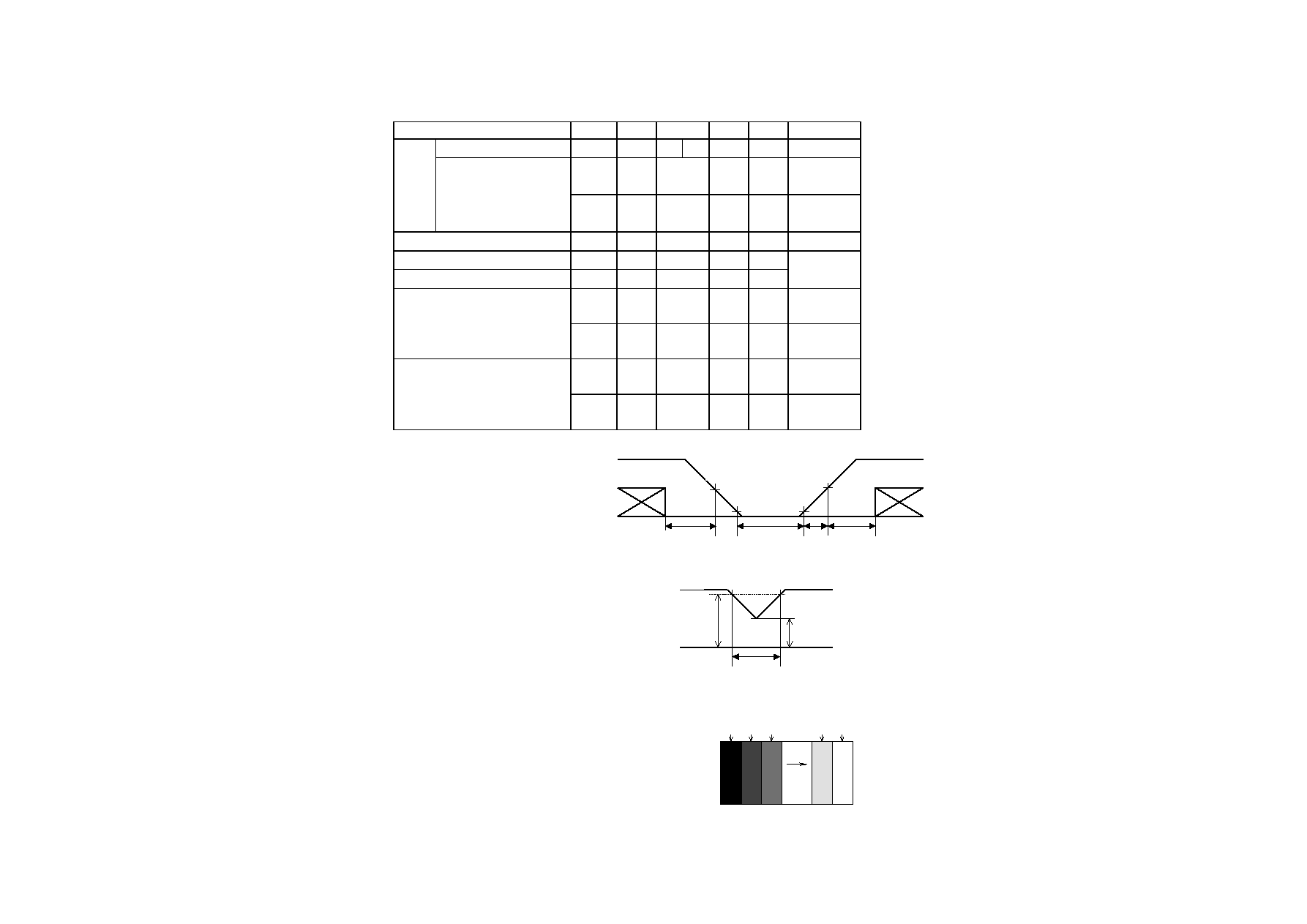
Each basic color can be displayed in 64 gray scales from 6 bit data signals. According to the combination of total 18 bit
data signals, the 262,144-color display can be achieved on the screen.
Basic Color
Basic Color
Basic Color
Basic Color
Gray Scale of Red
Gray Scale of Red
Gray Scale of Red
Gray Scale of Red
Gray Scale of Green
Gray Scale of Green
Gray Scale of Green
Gray Scale of Green
Gray Scale of Blue
Gray Scale of Blue
Gray Scale of Blue
Gray Scale of Blue
LD14702-13
9. Optical Characteristics
Ta=25, Vcc=+5V
Parameter
Symbol
Condition
Min
Typ
Max
Unit
Remark
Viewing Horizontal 21,22
60
70
-
Deg. Note1,4
Angle
Vertical
11
35
40
-
Deg.
Range
12
55
70
-
Deg.
=�
150
-
-
-
Contrast ratio
Best
Viewing
Angle
-
300
-
-
Note2,4
Response
Rise
r
=�
-
20
-
Note
3,4
Time
Decay
d
-
40
-
Chromaticity of
-
0.313
-
Note4
White
-
0.329
-
Luminance of white
280
350
-
cd/m
2
I
L
=6.0mArms
f=35kHz
White Unifomity
-
-
1.45
-
Note5
Horizontal 21,22
-
50
-
Deg.
11
-
40
-
Deg.
Viewing
Angle
range as a
Brightness
Definition
Vertical
12
50% of
the
maximum
brightness
-
35
-
Deg.
Note1
The measurement shall be executed 30 minutes after
li
ghting at
rating.
(condition:I
L
=
6.0mArms)
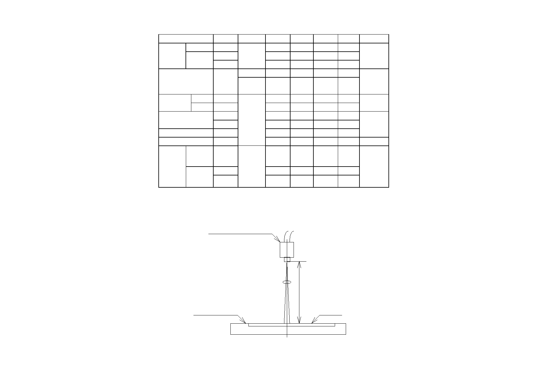
The optical characteristics shall be measured in a dark room or equivalent state
with the method shown in Fig.3 below.
Photodetector (BM-5A:TOPCON)
Fig.3 Optical characteristics measurement method
Center of the screen
- module
�
panel
LD14702-14
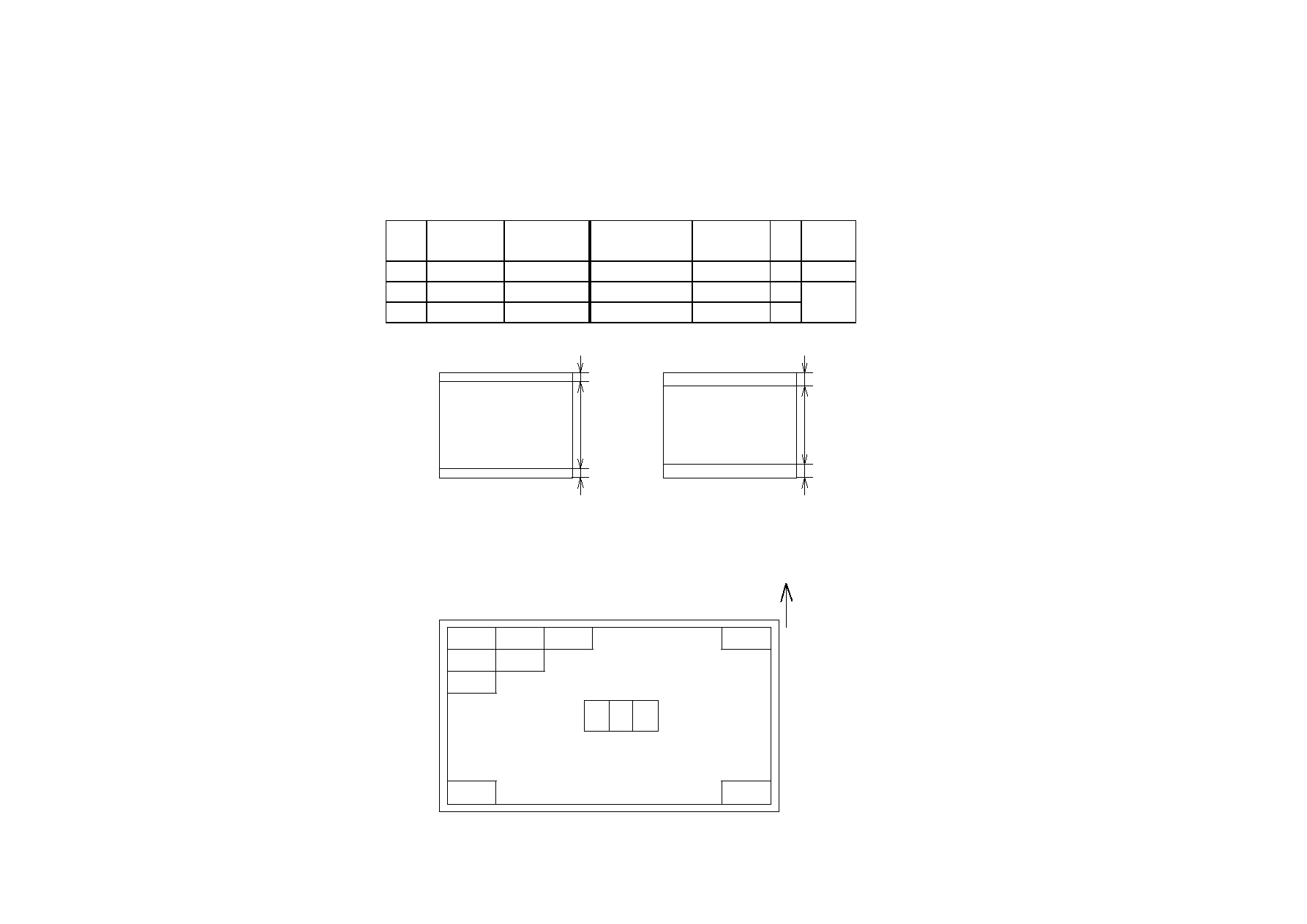
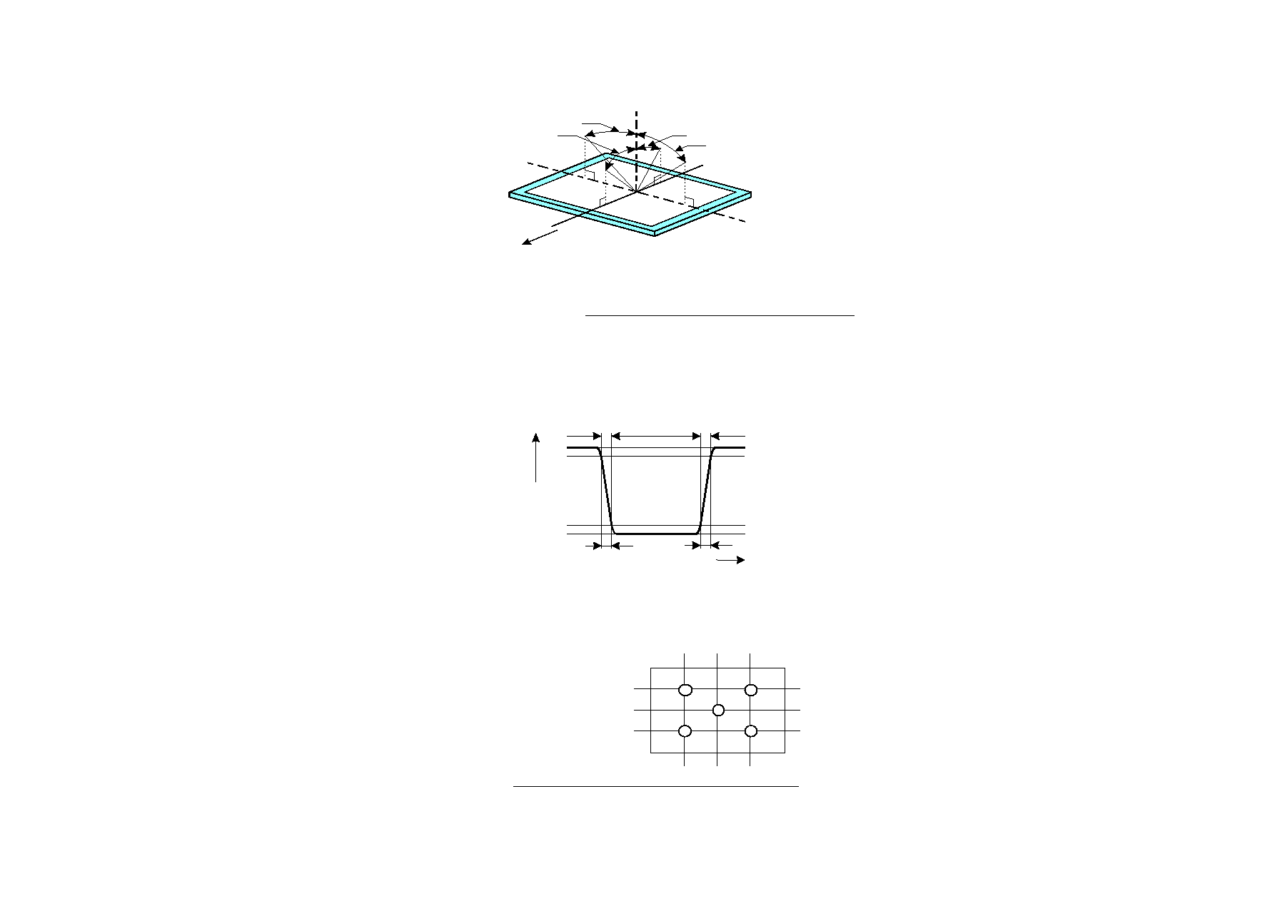
Note1Definitions of viewing angle range:
N o rm al lin e
22
12
11
21
6 o'clo ck d irectio n
Note2Definition of contrast ratio:
The contrast ratio is defined as the following.
Contrast Ratio (CR)
Note3Definition of response time:
The response time is defined as the following figure and shall be measured by
switching the input signal for "black" and "white" .
90%
100%
white
white
black
10%
0%
r
d
time
P
h
o
t
od
etect
or
ou
tp
ut
(r
el
ative V
a
l
u
e)
Note4This shall be measured at center of the screen.
Note5Definition of white uniformity:
White uniformity is defined as the
following with five measurements
(AE).
Luminance (brightness) with all pixels white
Luminance (brightness) with all pixels black
A
B
C
D
E
1 60
3 20
4 80
1 20
2 40
3 60
p ixel
p ixel
Maximum Luminance of five points (brightness)
Minimum Luminance of five points (brightness)
w
LD14702-15
10. Display Quantity
The display quality of the color TFT-LCD module shall be in compliance with the
Incoming Inspection Standard.
11Handling Precautions
a) Be sure to turn off the power supply when inserting or disconnecting the cable.
b) Be sure to design the cabinet so that the module can be installed without any extra stress such as
warp or twist.
c) Since the front polarizer is easily damaged, pay attention not to scratch it.
d) Wipe off water drop immediately. Long contact with water may cause discoloration or spots.
e) When the panel surface is soiled, wipe it with absorbent cotton or other soft cloth.
f) Since the panel is made of glass, it may break or crack if dropped or bumped on hard surface.
Handle with care.
g) Since CMOS LSI is used in this module, take care of static electricity and injure the human earth
when handling.
h) Laminated film is attached to the module front and back surface to prevent it from being scratched .
Peel the film off slowly , just before the use, with strict attention to electrostatic charges. Ionized
air shall be blown over during the action. Blow off 'dust' on the polarizer by using an ionized nitrogen
. i) The polarizer surface on the panel is treated with Anti-Glare for low reflection. In case of attaching
protective board over the LCD. Be careful about the optical interface fringe etc.
Which degrades display quality.
j)Do not expose the LCD panel to direct sunlight. Lightproof shade etc. should beattached when LCD panel is
used under such environment.
k) Connect GND to 4 place of mounting holes to stabilize against EMI and external noise.
l) There are high voltage portions on the backlight and very dangerous. Careless touch may lead to
electrical shock. When exchange lamps or service. Turn off the power without tail.
m) When handling LCD modules and assembling them into cabinets, please be noted that long-term
storage in the environment of oxidization or deoxidization gas and the use of such materials as reagent,
solvent, adhesive, resin, etc. which generate these gasses, may cause corrosion and discoloration of the
LCD modules.
n)Cold cathode fluorescent lamp in LCD panel contains a small amount of mercury, please follow local
ordinances or regulations for disposal.
12.Packing form
Piling number of cartons
Max
Packing quantity in one carton
20
Carton size [mm]
525 (W)�309(D)�377(H)
Total mass of one carton filled
with full modules
17.5kg
Packing form is shown
Fig.4
LD14702-16
13Reliability test items
No. Test item
Conditions
1 High temperature storage test
Ta=70 240h
2 Low temperature storage test
Ta= -30 240h
3 High temperature
& high humidity operation test
Ta=40 ; 95%RH 240h
(No condensation)
4 High temperature operation test
Ta=65 240h
5 Low temperature operation test
Ta= -10 240h
6 Vibration test
(non- operating)
Frequency: 1057Hz/Vibration width (one side):0.075mm
: 58500Hz/Gravity:9.8m/s
2
Sweep time : 11 minutes
Test period : 3 hours
(1 hour for each direction of X,Y,Z)
7 Shock test
(non- operating)
Max. gravity : 490m/s
2
Pulse width : 11ms, half sine wave
Direction : �X,�Y,�Z
once for each direction.
Result Evaluation Criteria
Under the display quality test conditions with normal operation state, these shall be no change
which may affect practical display function.
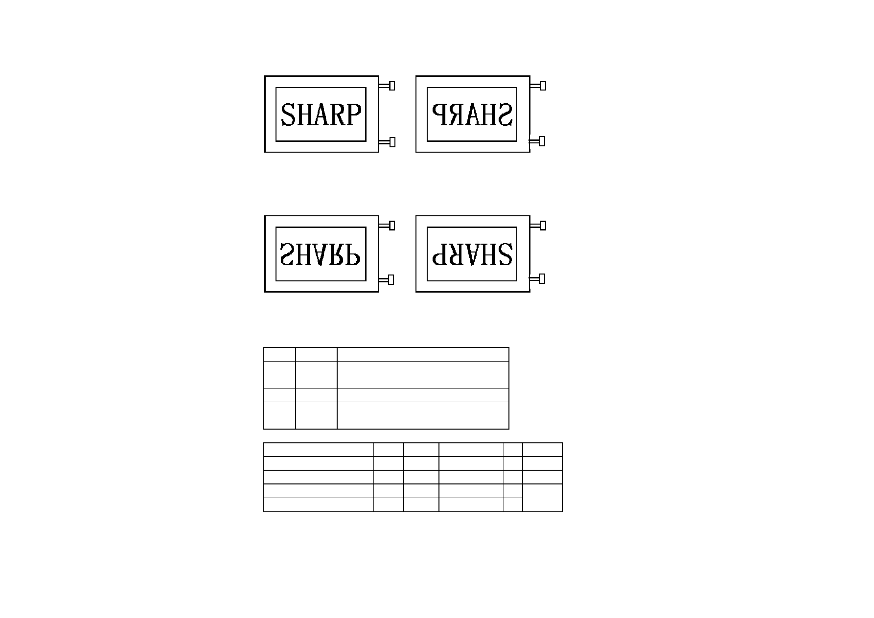
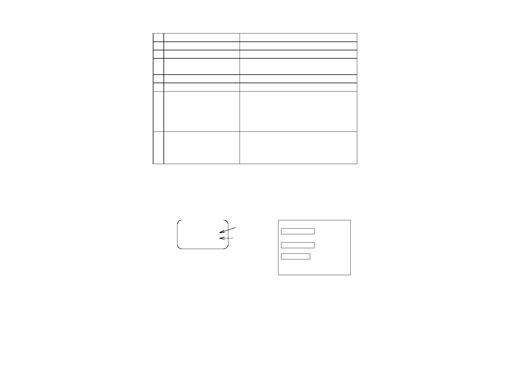
14Others
1) Label: Module
Packing box
Model.No Shipment Date Quntity
SHARP
LQ104V1DG21
27 XXXXXX A _
MADE IN
Model No.
Lot No.
2) Adjusting volume have been set optimally before shipment, so do not change any adjusted value.
If adjusted value is changed, the specification may not be satisfied.
3) Disassembling the module can cause permanent damage and should be strictly avoided.
4) Please be careful since image retention may occur when a fixed pattern is displayed for a long
time
5) If any problem occurs in relation to the description of this specification , it shall be resolved
through discussion with spirit of cooperation.
LQ104V1DG21
LQ104V1DG21
LQ104V1DG21
LQ104V1DG21
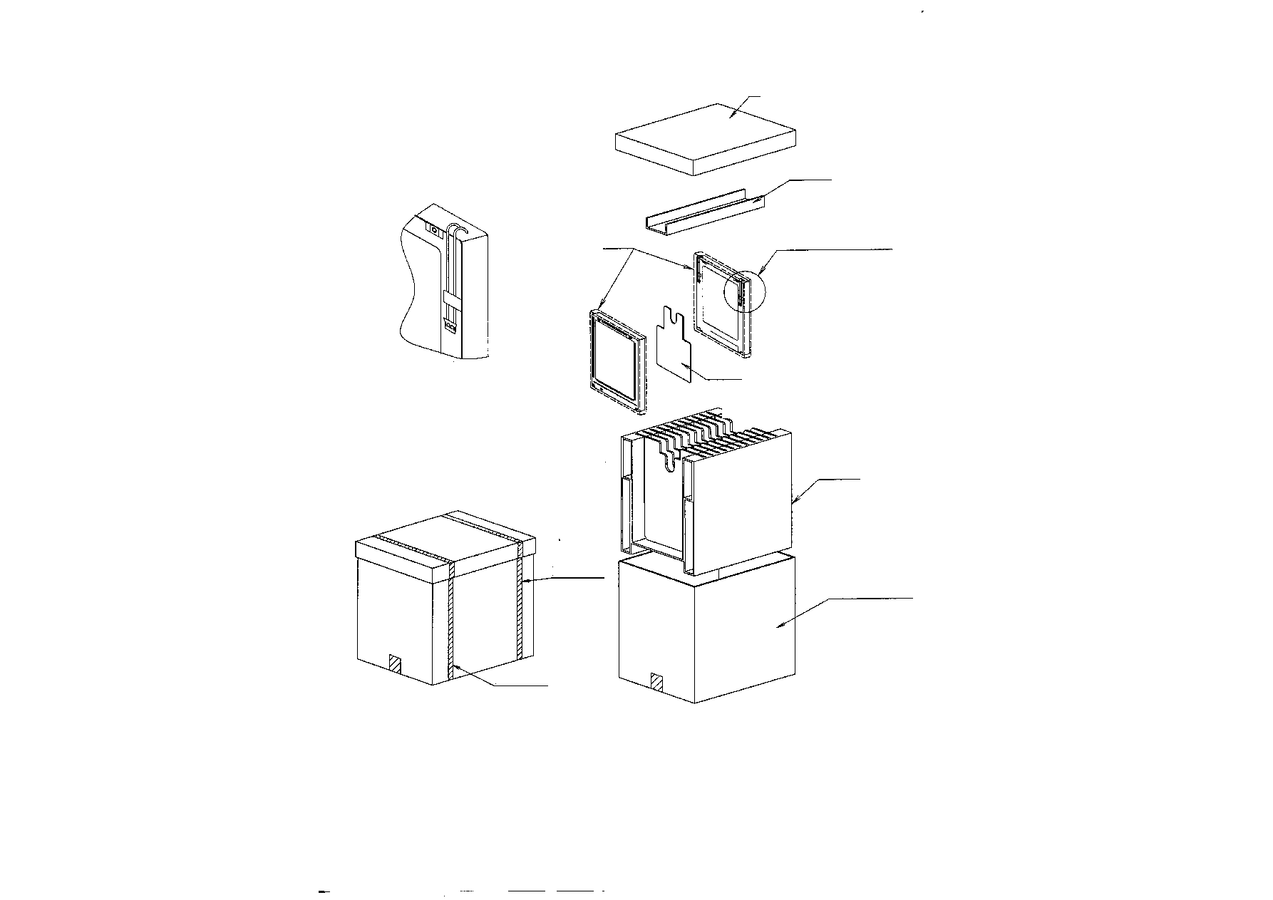
Fig.4 Packing Form
LD14702-17
Static electricity
protective sack
Ceiling Pad
Lid
Spacer
Master Carton
Bottom Pad
PP band
PP band
See Detail A
ENLARGED Detail A
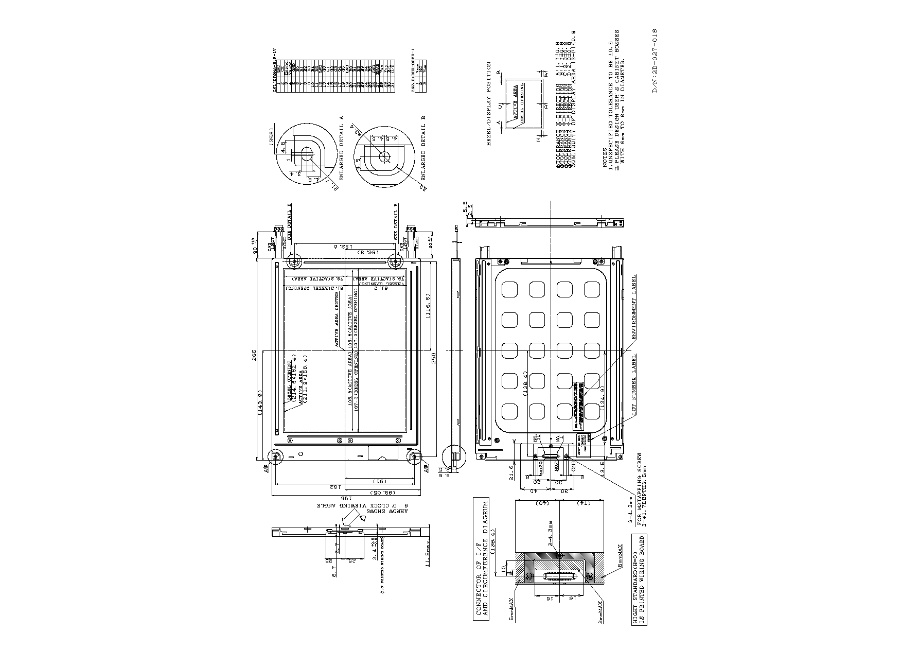
Fig.1 Outline Dimensions
LD14702-18