RECORDS OF REVISION
SPEC No.
DATE
S W Y
NOTE
No.
PAGE
June.
28.1995
-
-
1 st Issu
LD-7606A
.8, 1996
Al
3
Power Sequence is added.
- - - - - -
_____ _____ _____ _
2 n d
---------- ______ ______ ______ _ _ _ _ _ _ _
A2
5 6
Ripple Voltage is added.
- - - - - - - - _____ _____ _____
----- ----- _____ _____ _____ ___ .
A3
17
Inverter Pin numbers are added.
- - - - - -- ________ ___
_________ _____ ______ _____ ___ _____ __
6
1
- - - - - - - - _______
--- -- ______ __ ____ __
- - - - - - - - _____ ______
---______---- _____ _____ _______ _
_
_
- -- ----
_____ ______ ____
_ _ _ _
_____ __________ _____ _____ ___ _____ __
- - - - - - - - - - - - - - - ____
__________________ _ ___ _ _ _
- - - - - - - - _
_
_
_
_ _ _ _
_ _ _ _
_ _ _ _ _ _ _ _ _ _ _ _ _ _ _ _ _ _ _ _ _ _ _ _ . __ ____
- - - - _ _ _ _ - - - - _ _ _ _ _
---______-- __________ ________
_
--- ____ _ _ _ _ _ _ _ ____
----_--____ _____ _ _____ _ _____
- - - - - _ _ _ - - - - _
_ _ _ _
---______-- __________ __ ______ _ _ _ _ _ _ _
- - - - - -
______ _____ ____
_ _ _ _
- - - - - -- _ _ _ _ _ _ _ _ _ _ _ _ _ _ _ _ _ .
- - - - - _ _ _ _
_
_
_ _ _ _
_ _ _ _ -- --- _____ ___ ___ _ _
- - - - - _ _ _ _____ __ _ _ _
_ _ _ _
_ _ _ _ _ _ _ _ _ _
_ _ _ _ _ _ _
- - - - - - -
________ ___
_ _ _ _ _ _ _ _ _ _ _ _ _ _ _ _ _
_
_
- - - - - _ _ _ _ _ _ _ _ _ _ _
_ _ _ _ - -- -- _ _ _ _ _ _ _ _ _ _ _ _ _ _ _ _ _ _ _ _ _ ______ _
- - - - - - - - _ _ _ _ _ _ _ _ _
_ _ _ _
-------- _______________________ _
_
_
- - - - - - - - _ _ _ _ _ _ _ ____
_ _ _ _
-- -- _ _ _ _ _ _ _ _ _ _ _ _ _ _ _ _ _ _ _
--- --- ________ ___ ____
_ _ _ _
- - - -- _ _ _ _ _ _ _ _ _ _ _ _ _ _ _ _ _ _
_
_
- - - - - - -
- - - - - - - - - - - - - - - - _____
-----_________ _____ ______ _____ _
_
_
_ _ _ _ _ _ _ _ .
_ _ _ _
_ _ _ _ _ _ _ _ _ _ _ _ _ _ _ _ _
- - - - - - - - -
- _ _ _
_ _ _ _
_ _ _ _ _ _ _ _ _ _ _ _ _ _ _ _ _ _ _ _ _ _ _ ______ _
--- -- _
_
_
_
_
_ _ _ _
- - - -- _ _ _ _ _ _ _ _ _ _ _ _ _ _ _ _ _ _ _ _
_
_
- - - - - - -
_
- - - - - - _ _ _ _ _ _ _ _ _ _ _ _ _ _ _ _
_
- - - -
- - - _
_
_
_ _ _ _
-- ____________ __ _
_
_
- - - - - - - - _______ ____ ____
----_______ _ __________________ _
_
_
- - - - - - -
_________ __ _
- - - -- _ _ _ _ _ _ _ _ _ _ _ _ _ _ _ _ _
_
_
________ _
_
_ _ _ _
- - - -- _ -- _ _ _ _ _ _ _ _ _ _ _ _ _ _ _ ______
_ _ _ _ _ _ _ _ _ _
__________________________ _
- - - -- - -
--- ____ _ _
________________ ___ ___ ______ _______
- - - - - - -
____
_ _ _ _
-- ---------- _ ________ __ _____
- - - - - - _ _ _ _ _ _ _ _ _ _ _
-----_________________________ _
_
_
1
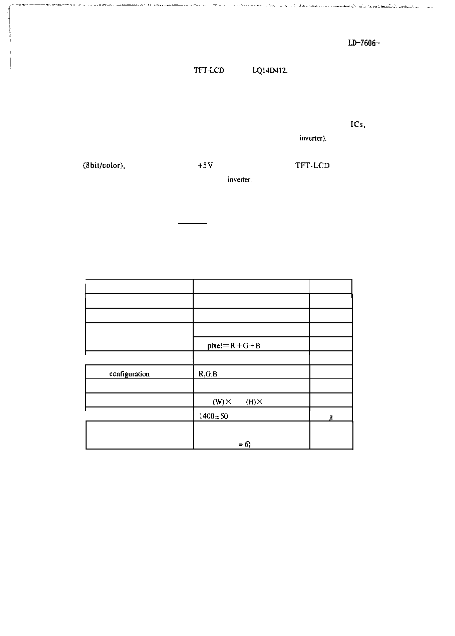
1. Application
q
This
specification applies to color
module,
2. Overview
This module is a color active matrix LCD module incorporating amorphous silicon TFT
(Thin Film Transistor). It is composed of a color TFT-LCD panel, driver
control
circuit, power supply circuit and a backlight unit (including a DC/AC
Graphics and texts
can be displayed on a 640X3X480 dots panel with 16M colors by supplying 24 bit data signal
four timing signals,
DC supply voltage for
panel driving and
supply voltage for a backlight-driving DC/AC
The TFT-LCD panel used for this module is a low-reflection and higher-color-saturation
type. Therefore, this module is suitable for the computer display and the multimedia use.
Optimum viewing direction is 6 o'clock.
3. Mechanical Specifications
Parameter
Specifications
unit
I
Display size
35 (13.8") Diagonal
cm
Active area
281 .3(H) X 207.8(V)
mm
Pixel format
640(H) X 480(V)
pixel
(1
dots)
Pixel pitch
0.44 (H) X 0.43 (V)
mm
Pixel
vertical stripe
Display mode
Normally white
Unit outline dimensions *1
330
242
18 (D)
mm
Mass
Surface treatment
Anti-glare and hard-coating 2H
(Haze value
*1. Note: excluding backlight cables.
Outline dimensions is shown in Fig. 1

3
] The 480 line
mode, the 400 line mode or the 350 line mode is selected by the polarity
combination of sync signals.
Mode
Polarity
Polarity
480 lines
Negative
Negative
400 lines
Negative
Positive
350 lines
Positive
Negative
The horizontal display start position is settled in accordance with a rising edge of
signal. In case
is
"Low" or "High", the horizontal start position is
determined as described in 7-2.
4-2. Backlight driving
CN2
Used connector:
o r
S5E-PH-SM3
Corresponding comector:
no.
Symbol
I/o
Function
Remark
1
v
I
+12V Supply Voltage
[ Note 1 ]
2
GND
3
v
Luminance Control Voltage
4
o
Lamp Status
[ Note 2 ]
5
I
Supply Voltage
[ Note 1
[Note
time of
is at the same time or later than that of
Power
VDD
There is no relation between above and Vcon timing.
[Note 2]
on or normally,
off or abnormally