 | –≠–ª–µ–∫—Ç—Ä–æ–Ω–Ω—ã–π –∫–æ–º–ø–æ–Ω–µ–Ω—Ç: LR36685 | –°–∫–∞—á–∞—Ç—å:  PDF PDF  ZIP ZIP |
Document Outline
- ˛ˇ
- ˛ˇ
- ˛ˇ
- ˛ˇ
- ˛ˇ
- ˛ˇ
- ˛ˇ
- ˛ˇ
- ˛ˇ
- ˛ˇ
- ˛ˇ
- ˛ˇ
- ˛ˇ
- ˛ˇ

1
DESCRIPTION
The RJ21P3AA0PT is a 1/1.8-type (8.93 mm) solid-
state image sensor that consists of PN photo-
diodes and CCDs (charge-coupled devices). With
approximately 3 370 000 pixels (2 152 horizontal x
1 567 vertical), the sensor provides a stable high-
resolution color image.
FEATURES
∑ Optical size : 8.93 mm (aspect ratio 4 : 3)
∑ Interline scan format
∑ Square pixel
∑ Number of image pixels : 2 096 (H) x 1 560 (V)
∑ Number of effective pixels : 2 080 (H) x 1 544 (V)
∑ Number of optical black pixels
≠ Horizontal : 2 front and 54 rear
≠ Vertical : 5 front and 2 rear
∑ Number of dummy bits
≠ Horizontal : 24
≠ Vertical : 2
∑ Pixel pitch : 3.45 µm (H) x 3.45 µm (V)
∑ R, G, and B primary color mosaic filters
∑ Supports monitoring mode
∑ Low fixed-pattern noise and lag
∑ No burn-in and no image distortion
∑ Blooming suppression structure
∑ Built-in output amplifier
∑ Built-in overflow drain voltage circuit and reset
gate voltage circuit
∑ Variable electronic shutter
∑ Package :
20-pin half-pitch DIP [Plastic]
(P-DIP020-0500)
Row space : 12.20 mm
PIN CONNECTIONS
PRECAUTIONS
∑ The exit pupil position of lens should be 30 to 55
mm from the top surface of the CCD.
∑ Refer to "PRECAUTIONS FOR CCD AREA
SENSORS" for details.
3 210 k effective pixels
2 080
1 544
8.93 mm
RJ21P3AA0PT
RJ21P3AA0PT
1/1.8-type Interline Color CCD
Area Sensor with 3 370 k Pixels
1
OD
2
GND
3
OFD
4
PW
5
ÿ
RS
6
NC
1
7
NC
2
8
ÿ
H1
9
NC
3
10
ÿ
H2
20
19
18
17
16
15
14
OS
GND
NC
5
NC
4
ÿ
V1A
ÿ
V1B
ÿ
V2
13 ÿ
V3A
12 ÿ
V3B
11 ÿ
V4
20-PIN HALF-PITCH WDIP
TOP VIEW
(P-DIP020-0500)
In the absence of confirmation by device specification sheets, SHARP takes no responsibility for any defects that may occur in equipment using any SHARP devices shown in
catalogs, data books, etc. Contact SHARP in order to obtain the latest device specification sheets before using any SHARP device.
BACK

2
RJ21P3AA0PT
PIN DESCRIPTION
SYMBOL
PIN NAME
OD
Output transistor drain
OS
Output signals
ÿ
RS
Reset transistor clock
ÿ
V1A
, ÿ
V1B
, ÿ
V2
, ÿ
V3A
, ÿ
V3B
, ÿ
V4
Vertical shift register clock
ÿ
H1
, ÿ
H2
Horizontal shift register clock
PW
P-well
GND
Ground
NC
1
, NC
2
, NC
3
, NC
4
, NC
5
No connection
Overflow drain
OFD
ABSOLUTE MAXIMUM RATINGS
(T
A
= +25∞C)
PARAMETER
SYMBOL
RATING
UNIT
Output transistor drain voltage
V
OD
0 to +18
V
Reset gate clock voltage
V
ÿRS
Internal output
V
Vertical shift register clock voltage
V
ÿV
V
PW
to +18
V
Horizontal shift register clock voltage
V
ÿH
≠0.3 to +12
V
Voltage difference between P-well and vertical clock
V
PW
-V
ÿV
≠27 to 0
V
Storage temperature
T
STG
≠40 to +85
∞C
Ambient operating temperature
T
OPR
≠20 to +70
∞C
2
NOTE
NOTES :
1.Do not connect to DC voltage directly.
When OFD is connected to GND, connect V
OD
to GND. Overflow drain clock is
applied below 24 Vp-p.
2.Do not connect to DC voltage directly.
When ÿ
RS
is connected to GND, connect V
OD
to GND. Reset gate clock is
applied below 8 Vp-p.
3.When clock width is below 10 µs, and clock duty factor is below 0.
1%, voltage difference between vertical clocks will be
below 26 V.
1
V
Internal output
V
OFD
Overflow drain voltage
3
V
0 to +18
V
ÿV
-V
ÿV
Voltage difference between vertical clocks

3
RJ21P3AA0PT
RECOMMENDED OPERATING CONDITIONS
PARAMETER
SYMBOL
MIN.
TYP.
MAX.
UNIT
NOTE
Ambient operating temperature
T
OPR
25.0
∞C
Output transistor drain voltage
V
OD
14.55
15.0
15.45
V
NOTES :
1.Use the circuit parameter indicated in "SYSTEM CONFIGURATION EXAMPLE", and do not connect to DC voltage directly.
2.V
PW
is set below V
ÿVL
that is low level of vertical shift register clock, or is used with the same power supply that is connected
to V
L
of V driver IC.
* To apply power, first connect GND and then turn on V
OD
. After turning on V
OD
, turn on V
PW
first and then turn on other
powers and pulses. Do not connect the device to or disconnect it from the plug socket while power is being applied.
1
V
22.8
21.5
20.7
V
ÿOFD
Overflow drain clock
P-well voltage
V
PW
≠8.0
V
ÿVL
V
2
Ground
GND
0.0
V
V
≠6.65
≠7.0
≠7.35
V
ÿV1AL
, V
ÿV1BL
, V
ÿV2L
V
ÿV3AL
, V
ÿV3BL
, V
ÿV4L
Vertical shift
register clock
LOW level
INTERMEDIATE level
HIGH level
V
ÿV1AI
, V
ÿV1BI
, V
ÿV2I
V
ÿV3AI
, V
ÿV3BI
, V
ÿV4I
V
ÿV1AH
, V
ÿV1BH
V
ÿV3AH
, V
ÿV3BH
14.55
0.0
15.0
15.45
V
V
LOW level
Horizontal shift
register clock
V
ÿH1L
, V
ÿH2L
≠0.05
0.0
+0.05
V
HIGH level
V
ÿH1H
, V
ÿH2H
4. 5
4. 8
5. 5
V
1
V
5.5
4.8
4.5
V
ÿRS
Reset gate clock
p-p level
Reset gate clock frequency
f
ÿRS
18.00
MHz
Horizontal shift register clock frequency
f
ÿH1
, f
ÿH2
18.00
MHz
Vertical shift register clock frequency
f
ÿV1A
, f
ÿV1B
, f
ÿV2
f
ÿV3A
, f
ÿV3B
, f
ÿV4
7.50
kHz
p-p level

RJ21P3AA0PT
4
CHARACTERISTICS
(Drive method : 1/30 s frame accumulation)
(T
A
= +25∞C, Operating conditions : The typical values specified in "RECOMMENDED OPERATING CONDITIONS".
Color temperature of light source : 3 200 K, IR cut-off filter (CM-500, 1 mmt) is used.)
PARAMETER
SYMBOL
MIN.
TYP.
MAX.
UNIT
NOTE
Standard output voltage
V
O
150
mV
2
Photo response non-uniformity
PRNU
10
%
3
Saturation output voltage
V
SAT
450
530
mV
4
Dark output voltage
V
DARK
0.5
3.0
mV
1, 6
Dark signal non-uniformity
DSNU
0.5
2.0
mV
1, 7
Sensitivity (green channel)
R (G)
130
160
mV
8
Smear ratio
SMR
≠90
≠82
dB
9
Image lag
AI
1.0
%
10
Blooming suppression ratio
ABL
1 000
11
Output transistor drain current
I
OD
4.0
8.0
mA
NOTES :
∑ Within the recommended operating conditions of V
OD
,
V
OFD
of the internal output satisfies with ABL larger than
1 000 times exposure of the standard exposure conditions,
and V
SAT
larger than 320 mV.
1.T
A
= +60∞C
2.The average output voltage of G signal under uniform
illumination. The standard exposure conditions are
defined as when Vo is 150 mV.
3.The image area is divided into 10 x 10 segments under
the standard exposure conditions. Each segment's
voltage is the average output voltage of all pixels within
the segment. PRNU is defined by (Vmax ≠ Vmin)/Vo,
where Vmax and Vmin are the maximum and minimum
values of each segment's voltage respectively.
4.The image area is divided into 10 x 10 segments.
Each
segment's voltage is the average output voltage of all
pixels within the segment. V
SAT
is the minimum
segment's voltage under 10 times exposure of the
standard exposure conditions. The operation of OFDC is
high. (for still image capturing)
5.The image area is divided into 10 x 10 segments.
Each
segment's voltage is the average output voltage of all
pixels within the segment. V
SAT
is the minimum
segment's voltage under 10 times exposure of the
standard exposure conditions. The operation of OFDC is
low.
6.The average output voltage under non-exposure
conditions.
7.The image area is divided into 10 x 10 segments under
non-exposure conditions. DSNU is defined by (Vdmax ≠
Vdmin), where Vdmax and Vdmin are the maximum and
minimum values of each segment's voltage respectively.
8.The average output voltage of G signal when a 1 000
lux light source with a 90% reflector is imaged by a lens
of F4, f50 mm.
9.The sensor is exposed only in the central area of V/10
square with a lens at F4, where V is the vertical image
size. SMR is defined by the ratio of the output voltage
detected during the vertical blanking period to the
maximum output voltage in the V/10 square.
10.The sensor is exposed at the exposure level
corresponding to the standard conditions. AI is defined
by the ratio of the output voltage measured at the 1st
field during the non-exposure period to the standard
output voltage.
11.The sensor is exposed only in the central area of V/10
square, where V is the vertical image size. ABL is
defined by the ratio of the exposure at the standard
conditions to the exposure at a point where blooming is
observed.
5
mV
400
320
RJ21P3AA0PT
5
PIXEL STRUCTURE
COLOR FILTER ARRAY
(1, 1 560)
(2 096, 1 560)
(1, 1)
(2 096, 1)
ÿ
V3B
ÿ
V1A
ÿ
V3B
ÿ
V1B
ÿ
V3B
ÿ
V1B
ÿ
V3B
ÿ
V1B
ÿ
V3A
ÿ
V1B
ÿ
V3B
ÿ
V1B
ÿ
V3B
ÿ
V1B
ÿ
V3B
ÿ
V1A
ÿ
V3B
ÿ
V1B
ÿ
V3B
ÿ
V1B
ÿ
V3B
ÿ
V1B
ÿ
V3B
ÿ
V1B
ÿ
V3A
ÿ
V1B
ÿ
V3B
ÿ
V1B
ÿ
V3B
ÿ
V1B
ÿ
V3B
ÿ
V1A
ÿ
V3B
ÿ
V1B
ÿ
V3B
ÿ
V1B
G
R
G
R
G
R
G
R
G
R
G
R
G
R
G
R
G
R
B
G
B
G
B
G
B
G
B
G
B
G
B
G
B
G
B
G
B
G
B
G
B
G
B
G
B
G
B
G
B
G
B
G
B
G
B
G
B
G
B
G
B
G
B
G
B
G
B
G
B
G
B
G
B
G
B
G
B
G
B
G
B
G
B
G
B
G
B
G
B
G
B
G
B
G
B
G
B
G
B
G
B
G
B
G
B
G
B
G
B
G
B
G
B
G
B
G
B
G
B
G
B
G
B
G
B
G
G
R
G
R
G
R
G
R
G
R
G
R
G
R
G
R
G
R
G
R
G
R
G
R
G
R
G
R
G
R
G
R
G
R
G
R
G
R
G
R
G
R
G
R
G
R
G
R
G
R
G
R
G
R
G
R
G
R
G
R
G
R
G
R
G
R
G
R
G
R
G
R
G
R
G
R
G
R
G
R
G
R
G
R
G
R
G
R
G
R
G
R
G
R
G
R
G
R
G
R
G
R
G
R
G
R
G
R
B
G
B
G
B
G
B
G
B
G
B
G
B
G
B
G
B
G
B
G
B
G
B
G
B
G
B
G
B
G
B
G
B
G
B
G
B
G
B
G
B
G
B
G
B
G
B
G
B
G
B
G
B
G
B
G
B
G
B
G
B
G
B
G
B
G
B
G
B
G
B
G
B
G
B
G
B
G
B
G
B
G
B
G
B
G
B
G
B
G
B
G
B
G
B
G
B
G
B
G
B
G
B
G
B
G
B
G
G
R
G
R
G
R
G
R
G
R
G
R
G
R
G
R
G
R
G
R
G
R
G
R
G
R
G
R
G
R
G
R
G
R
G
R
G
R
G
R
G
R
G
R
G
R
G
R
G
R
G
R
G
R
G
R
G
R
G
R
G
R
G
R
G
R
G
R
G
R
G
R
G
R
G
R
G
R
G
R
G
R
G
R
G
R
G
R
G
R
G
R
G
R
G
R
G
R
G
R
G
R
G
R
G
R
G
R
B
G
B
G
B
G
B
G
B
G
B
G
B
G
B
G
B
G
B
G
B
G
B
G
B
G
B
G
B
G
B
G
B
G
B
G
B
G
B
G
B
G
B
G
B
G
B
G
B
G
B
G
B
G
B
G
B
G
B
G
B
G
B
G
B
G
B
G
B
G
B
G
B
G
B
G
B
G
B
G
B
G
B
G
B
G
B
G
B
G
B
G
B
G
B
G
B
G
B
G
B
G
B
G
B
G
B
G
G
R
G
R
G
R
G
R
G
R
G
R
G
R
G
R
G
R
G
R
G
R
G
R
G
R
G
R
G
R
G
R
G
R
G
R
G
R
G
R
G
R
G
R
G
R
G
R
G
R
G
R
G
R
G
R
G
R
G
R
G
R
G
R
G
R
G
R
G
R
G
R
G
R
G
R
G
R
G
R
G
R
G
R
G
R
G
R
G
R
G
R
G
R
G
R
G
R
G
R
G
R
G
R
G
R
G
R
B
G
B
G
B
G
B
G
B
G
B
G
B
G
B
G
B
G
B
G
B
G
B
G
B
G
B
G
B
G
B
G
B
G
B
G
B
G
B
G
B
G
B
G
B
G
B
G
B
G
B
G
B
G
B
G
B
G
B
G
B
G
B
G
B
G
B
G
B
G
B
G
B
G
B
G
B
G
B
G
B
G
B
G
B
G
B
G
B
G
B
G
B
G
B
G
B
G
B
G
B
G
B
G
B
G
B
G
G
R
G
R
G
R
G
R
G
R
G
R
G
R
G
R
G
R
G
R
G
R
G
R
G
R
G
R
G
R
G
R
G
R
G
R
G
R
G
R
G
R
G
R
G
R
G
R
G
R
G
R
G
R
G
R
G
R
G
R
G
R
G
R
G
R
G
R
G
R
G
R
G
R
G
R
G
R
G
R
G
R
G
R
G
R
G
R
G
R
Pin arrangement
of the vertical
readout clock
1 pin
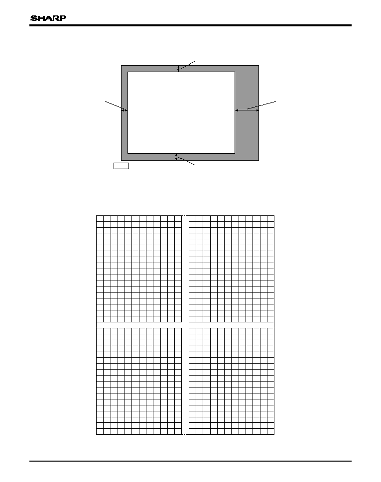
OPTICAL BLACK
(5 PIXELS)
OPTICAL BLACK
(2 PIXELS)
OPTICAL BLACK
(54 PIXELS)
OPTICAL BLACK
(2 PIXELS)
2 096 (H) x 1 560 (V)
RJ21P3AA0PT
6
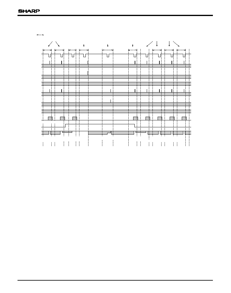
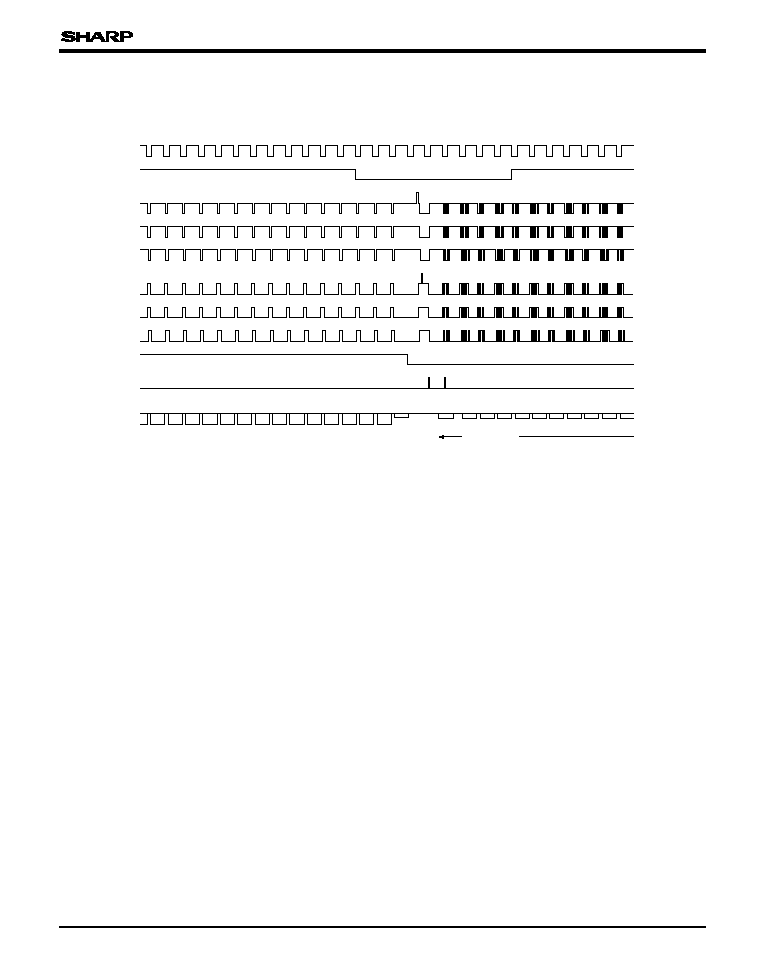
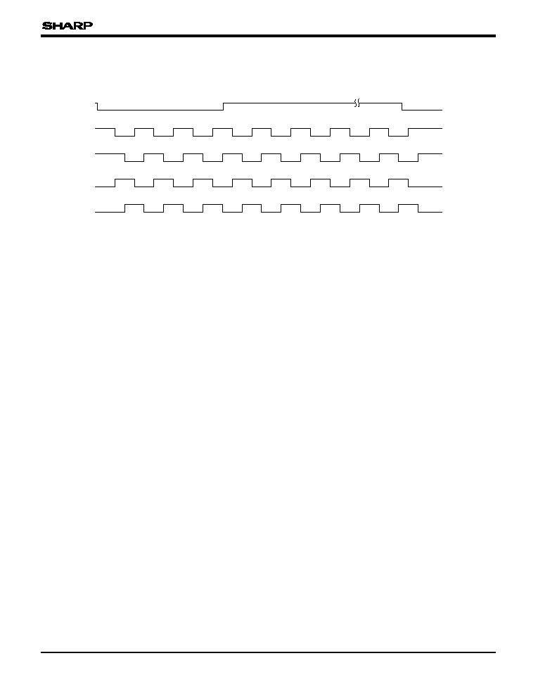
TIMING CHART
NOTES :
1.Do not use these signals immediately after field accumulation mode is transferred to frame
accumulation mode for still image capturing.
2.Do not use these signals immediately after frame accumulation mode is transferred to field
accumulation mode for monitoring image.
* Start the exposure period after 10 ms later that OFDC is high, and finish before change swept
transfer.
* Apply at least an OFD shutter pulse to OFD in each field accumulation mode.
;
;
;
;
;
;
;
;
;
;
;
;
;
;
ÿ
V3A
ÿ
V2
ÿ
V1B
ÿ
V1A
VD
TIMING CHART EXAMPLE
OS
OFDC
ÿ
OFD
ÿ
V4
ÿ
V3B
227.5
227.5
227.5
848
227.5
1
Pulse diagram in more detail is shown in the figure q to r after next page.
Field accumulation mode
At first frame
accumulation mode
Frame accumulation
mode
At first field
accumulation mode
Field accumulation mode
q
w
e
r
q
q'
q
q'
455 1
455 1
455 1
455 1
q
'
(Number of
vertical line)
(at OFD shutter operation)
(1, 3, 5, 7, 9...)
(2, 4, 6, 8, 10...)
(5, 12, 19...)
Not for use
(NOTE 2)
(5, 12, 19..)
(5, 12, 19..)
(5, 12, 19..)
Frame accumulation mode
Field accumulation mode
Not for use
(NOTE 1)
Not for use
(NOTE 1)
Field accumulation
mode
848 1
RJ21P3AA0PT
7
OS
OB3
5
GB RG GB RG GB RG
1531
1545
1559
1524
1538
1552
GB
RG GB RG
GB RG GB RG GB RG GB
RG GB RG
1503
1517
1496
1510
RG GB RG
1475
1489
1482
ÿ
V3A
ÿ
V2
ÿ
V3B
ÿ
V1B
ÿ
V1A
HD
VD
ÿ
OFD
OFDC
ÿ
V4
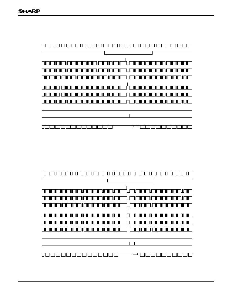
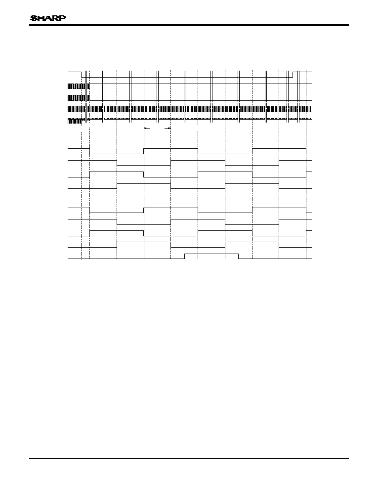
q VERTICAL TRANSFER TIMING øFIELD ACCUMULATION MODE°
217 218 219 220 221 222 223 224 225 226 227 228 229 230 231 232 233 234 235 236 237 238 239 240 241 242 243 244
12
26
19
40
54
33
47
68
61
2 640 clk/H
ÿ
V3A
ÿ
V2
ÿ
V3B
OS
ÿ
V1B
ÿ
V1A
HD
VD
ÿ
OFD
OFDC
ÿ
V4
444 445 446 447 448 449 450 451 452 453 454 455 1
2
3
4
5
6
7
8
9
10 11 12 13 14 15 16
1531
1545
1559
1524
1538
1552
5
OB3
12
19
26
33
40
47
54
61
68
1503
1517
1496
1510
GB RG GB RG GB RG GB RG GB RG GB RG GB RG
RG GB RG
GB
RG
GB RG
GB RG GB
1475
1489
1482
1468
q' VERTICAL TRANSFER TIMING øFIELD ACCUMULATION MODE°
2 640 clk/H
RJ21P3AA0PT
8
ÿ
V3A
ÿ
V2
ÿ
V3B
OS
ÿ
V1B
ÿ
V1A
HD
VD
ÿ
OFD
OFDC
ÿ
V4
451 452 453 454 455 1
2
3
4
5
6
7
8
9
... 61 62 63 64 65 66 67 68 69 70 71 72 73
RG RG RG RG
OB2 OB4
1
3
5
7
Not for use
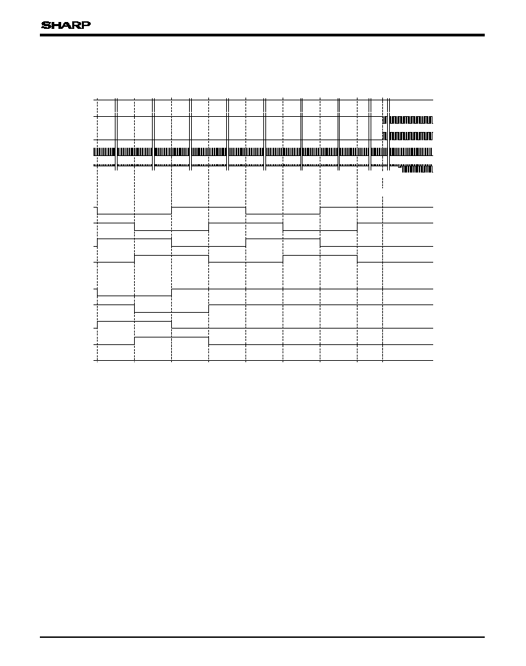
w VERTICAL TRANSFER TIMING øAT FIRST FRAME ACCUMULATION MODE°
2 640 clk/H
Charge swept transfer (2 112 stages)
ÿ
OFD
ÿ
V3A
OFDC
ÿ
V4
ÿ
V3B
ÿ
V2
ÿ
V1B
ÿ
V1A
VD
HD
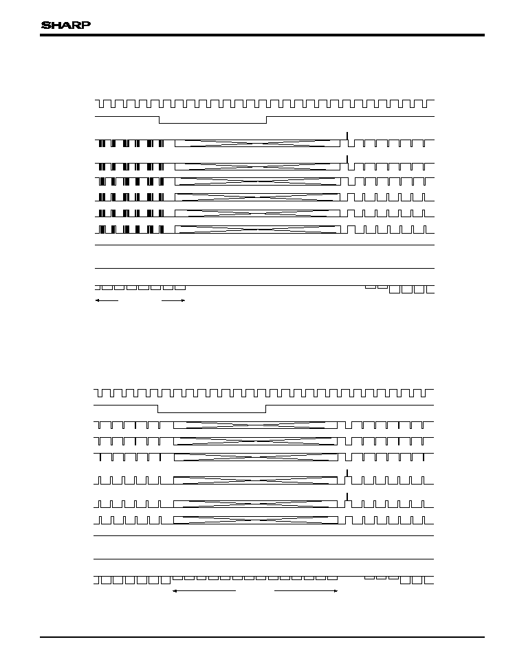
e VERTICAL TRANSFER TIMING øFRAME ACCUMULATION MODE°
844 845 846 847 848 1
2
3
4
5
6
7
8
9
... 61 62 63 64 65 66 67 68 69 70 71 72 73
OS
OB1 OB3 OB5
2
4
6
GB
RG RG RG RG RG RG
GB GB
Not for use
Charge swept transfer (2 112 stages)
1557
1555
1559
1549
1553
1551
2 640 clk/H
* Do not use the frame signals immediately after field accumulation mode is transferred to frame
accumulation mode.
RJ21P3AA0PT
9
ÿ
OFD
ÿ
V3A
OFDC
ÿ
V4
ÿ
V3B
ÿ
V2
ÿ
V1B
ÿ
V1A
VD
HD
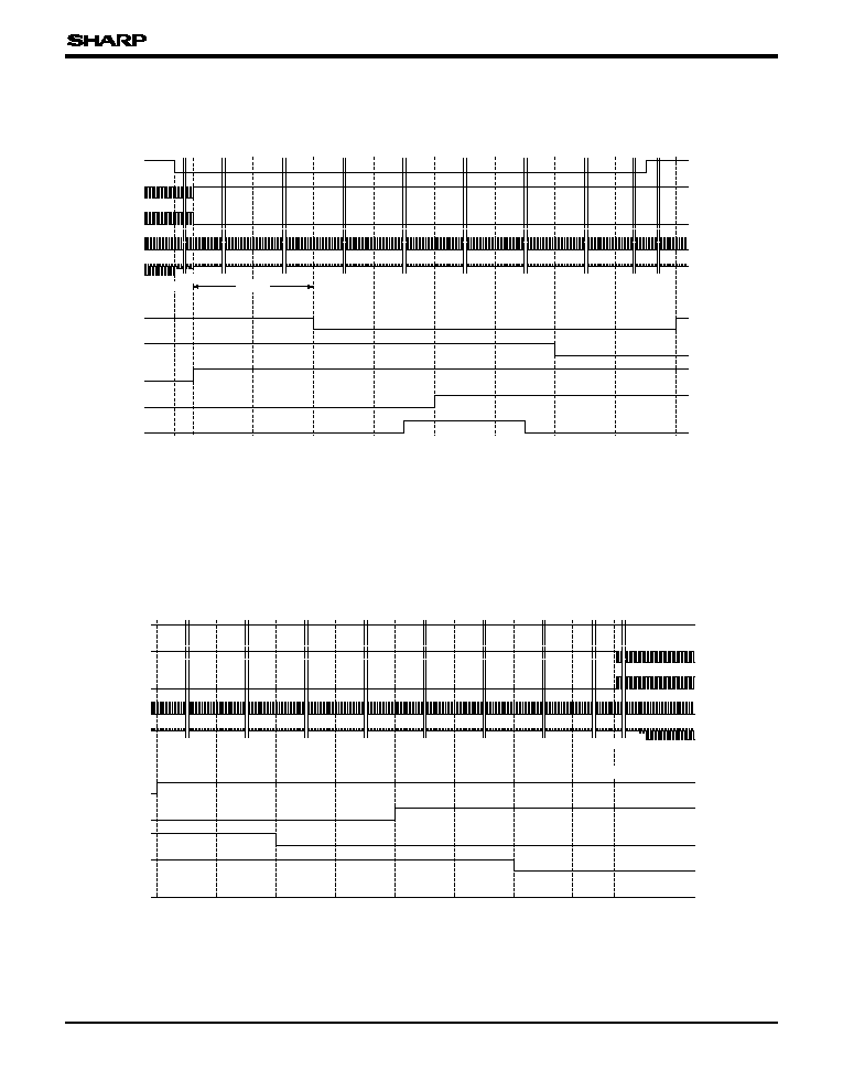
r VERTICAL TRANSFER TIMING øAT FIRST FIELD ACCUMULATION MODE°
837 838 839 840 841 842 843 844 845 846 847 848 1
2
3
4
5
6
7
8
9
10 11 12 13 14 15 16
OS
GB
GB
GB
GB
GB
GB
GB
GB
GB
GB
GB
GB
GB
GB
Not for use
1534
OB2
1536
1538
1540
1542
1544
1546
1548
1550
1552
1554
1556
1558
1560
2 640 clk/H
* Do not use the field signals immediately after frame accumulation mode is transferred to field
accumulation mode for monitoring image.

RJ21P3AA0PT
10
38.9 µs (698 bits)
57.6 µs (1 034 bits)
(126 bits)
(126 bits)
866
ÿ
V3A
ÿ
V4
ÿ
V3B
ÿ
V2
ÿ
V1A
HD
260
222
194
250
166
260
2640
(0)
2640
(0)
908
1160
1034
992
698 824
950
7.02 µs
7.02 µs
ÿ
V1B
READOUT TIMING øFIELD ACCUMULATION MODE°
38.9 µs (698 bits)
(126 bits)
ÿ
V3A
ÿ
V3B
ÿ
V4
ÿ
V2
ÿ
V1A
ÿ
V1B
HD
7.02 µs
READOUT TIMING øFRAME ACCUMULATION MODE°
w
57.6 µs (1 034 bits)
(126 bits)
ÿ
V3A
ÿ
V3B
ÿ
V4
ÿ
V2
ÿ
V1A
ÿ
V1B
HD
7.02 µs
e
260
222
194
250
166
260
16
16
36
36
2640
(0)
2640
(0)
908
992
698 824
866
950
260
222
194
250
166
260
16
36
36
908
992
866
950
950
1160
1034
2640
(0)
2640
(0)
RJ21P3AA0PT
11
OS
ÿ
RS
ÿ
H2
ÿ
H1
HD
HORIZONTAL TRANSFER TIMING øFIELD ACCUMULATION MODE°-1
1 clk = 55.7 ns (= 1/18.0 MHz)
2640
(0) 54
82
110
138
166
194
222
250
260 278
28 clk
4-stage transfer
3-stage transfer
OFD
ÿ
V4
ÿ
V2
ÿ
V1A
ÿ
V1B
ÿ
V3A
ÿ
V3B
ÿ
V4
ÿ
V2
ÿ
V1A
ÿ
V1B
ÿ
V3A
ÿ
V3B
152
208
(= 1.56 µs)
OB (54)
2096
* Keep over 1.56 µs when vertical transfer clock pulse is overlapping.
RJ21P3AA0PT
12
OS
ÿ
RS
ÿ
H2
ÿ
H1
HD
HORIZONTAL TRANSFER TIMING øFIELD ACCUMULATION MODE°-2
1 clk = 55.7 ns (= 1/18.0 MHz)
306
278
334
362
390
418
446
474
518
OFD
ÿ
V4
ÿ
V2
ÿ
V1A
ÿ
V1B
ÿ
V3A
ÿ
V3B
ÿ
V4
ÿ
V2
ÿ
V1A
ÿ
V1B
ÿ
V3A
ÿ
V3B
4-stage transfer
3-stage transfer
OB (2)
PRE SCAN (24)
OUTPUT (2 096) 1
* Keep over 1.56 µs when vertical transfer clock pulse is overlapping.
RJ21P3AA0PT
13
OS
ÿ
RS
ÿ
H2
ÿ
H1
HD
HORIZONTAL TRANSFER TIMING øFRAME ACCUMULATION MODE°-1
1 clk = 55.7 ns (= 1/18.0 MHz)
2640
(0) 54
82
110
138
166
194
222
250
260 278
ÿ
V4
OFD
ÿ
V2
ÿ
V1A
ÿ
V1B
ÿ
V3A
ÿ
V3B
152
208
(= 3.11 µs)
56 clk
OB (54)
2096
OS
ÿ
RS
ÿ
H2
ÿ
H1
HD
HORIZONTAL TRANSFER TIMING øFRAME ACCUMULATION MODE°-2
1 clk = 55.7 ns (= 1/18.0 MHz)
278
306
334
362
390
418
446
474
508
ÿ
V4
OFD
ÿ
V2
ÿ
V1A
ÿ
V1B
ÿ
V3A
ÿ
V3B
OB (2)
PRE SCAN (24)
OUTPUT (2 096) 1
* Keep over 3.11 µs when vertical transfer clock pulse is overlapping.
* Keep over 3.11 µs when vertical clock pulse is overlapping.
ÿ
V1A
ÿ
V1B
ÿ
V4
ÿ
V3A
ÿ
V3B
ÿ
V2
HD
CHARGE SWEPT TRANSFER TIMING øFRAME ACCUMULATION MODE°
w, e 2H
1
2
3
2112
2111
2110
4H
5H
65H
66H
3H
0
260
2640
56
96
176
216
136
56
96
176
216
136
116
76
156
196
116
76
156
196
2616 16
2636 36
2636 36
2616 16
∑ ∑ ∑ ∑ ∑ ∑ ∑
∑ ∑ ∑ ∑ ∑ ∑ ∑
RJ21P3AA0PT
14
* Keep over 1.56 µs when vertical transfer clock pulse of charge swept transfer is overlapping.
RJ21P3AA0PT
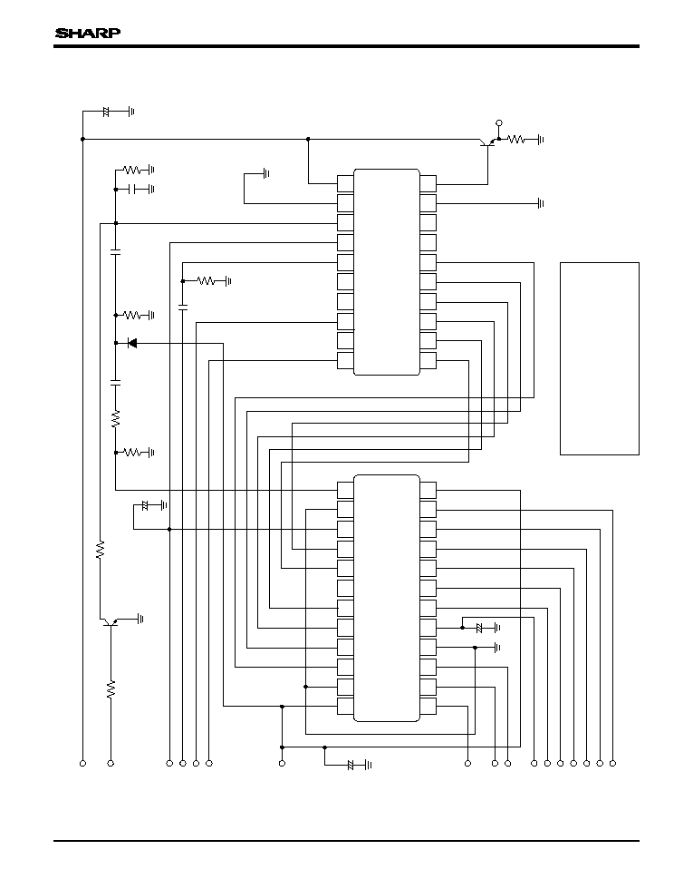
15
OD
PW
OFD
ÿ
V2
ÿ
V1B
ÿ
V3A
ÿ
V3B
ÿ
V4
GND
NC
1
NC
2
ÿ
H1
NC
3
ÿ
H2
OS
GND
NC
5
NC
4
ÿ
V1A
ÿ
RS
V
3B
V
3A
V
1B
V
1A
V
Ma
V
H
V
4
V
2
V
L
V
Mb
POFD
NC
V
H
ÿ
H2
VH
1BX
V
3X
V
2X
VH
3BX
V
4X
V
1X
VH
3AX
VH
1AX
+V
DD
OFDX
ÿ
H1
ÿ
RS
V
L
(V
PW
)
CCD
OUT
V
OFDH
VH
3BX
OFDX
V
2X
V
1X
V
3X
V
DD
GND
V
4X
VH
3AX
VH
1BX
VH
1AX
+
+
1
2
3
4
5
6
7
8
12
24
23
22
21
20
19
18
17
13
11
14
10
15
9
16
2
3
4
5
6
7
8
19
18
1
20
17
16
15
14
13
9
10
12
11
LR36685
RJ21P3AA0PT
(*1)
(*1)
V
OD
OFDC
270
pF
100 $
1 M$
1 M$
5.6 k$
47 k$
47 µF
0. 1 µF
1.0 µF
0.01 µF
+
+
100 k$
33 k$
Be
sure
to
use
the
parameter
indicated
in
this
circuit
example.
(*1)
ÿ
RS
,
OFD
:
Do
not
connect
to
DC
voltage
directly.
SYSTEM CONFIGURATION EXAMPLE
RJ21P3AA0PT
16
;;;;;;;;;;;;;;;;;;;;;;;;;;;;;;;;;;;;;;;;;;;;;;;;;;;;;;;;;;;;;;;;;;;;;;
;;;;;;;;;;;;;;;;;;;;;;;;;;;;;;;;;;;;;;;;;;;;;;;;;;;;;;;;;;;;;;;;;;;;;;
;;;;;;;;;;;;;;;;;;;;;;;;;;;;;;;;;;;;;;;;;;;;;;;;;;;;;;;;;;;;;;;;;;;;;;
;;;;;;;;;;;;;;;;;;;;;;;;;;;;;;;;;;;;;;;;;;;;;;;;;;;;;;;;;;;;;;;;;;;;;;
;;;;;;;;;;;;;;;;;;;;;;;;;;;;;;;;;;;;;;;;;;;;;;;;;;;;;;;;;;;;;;;;;;;;;;
;;;;;;;;;;;;;;;;;;;;;;;;;;;;;;;;;;;;;;;;;;;;;;;;;;;;;;;;;;;;;;;;;;;;;;
;;;;;;;;;;;;;;;;;;;;;;;;;;;;;;;;;;;;;;;;;;;;;;;;;;;;;;;;;;;;;;;;;;;;;;
;;;;;;;;;;;;;;;;;;;;;;
;;;;;;;;;;;;;;;;;;;;;;
;;;;;;;;;;;;;;;;;;;;;;
;;;;;;;;;;;;;;;;;;;;;;
;;;;;;;;;;;;;;;;;;;;;;
;;;;;;;;;;;;;;;;;;;;;;
;;;;;;;;;;;;;;;;;;;;;;
;;;;;;;;;;;;;;;;;;;;;;
;;;;;;;;;;;;;;;;;;;;;;
;;;;;;;;;;;;;;;;;;;;;;
6.9
±0.075
0.4
±0.4
6
±0.075
0.4
±0.4
11.2
±0.1
(2)
12
±0.1
20
11
Center of effective imaging area
and center of package
Rotation error of die : ¨ = 1.0∞
MAX.
( 1 : Effective imaging area)
( 2 : Lid's size)
12.2
±0.1
Refractive index : nd = 1.5
0.5
±0.05
(2)
1.41
±0.025
0.25
±0.1
12.2
0.04
0.02
0.02
(1)
(1)
A'
A
A'
20-0.64
TYP.
20-0.3
TYP.
P-1.27
TYP.
0.2 M
3.5
±0.1
2.4
±0.1
2.9
±0.1
+0.3
≠0
Glass Lid
Package
CCD
13.8
±0.1
13
±0.1
(2)
1
10
CCD
¨
A
20 DIP (P-DIP020-0500)
(Unit : mm)
PACKAGE OUTLINES
RJ21P3AA0PT
17
PRECAUTIONS FOR CCD AREA SENSORS
1. Package Breakage
In order to prevent the package from being broken,
observe the following instructions :
1) The CCD is a precise optical component and
the package material is ceramic or plastic.
Therefore,
¯ Take care not to drop the device when
mounting, handling, or transporting.
¯ Avoid giving a shock to the package.
Especially when leads are fixed to the socket
or the circuit board, small shock could break
the package more easily than when the
package isn't fixed.
2) When applying force for mounting the device or
any other purposes, fix the leads between a
joint and a stand-off, so that no stress will be
given to the jointed part of the lead. In addition,
when applying force, do it at a point below the
stand-off part.
(In the case of ceramic packages)
≠ The leads of the package are fixed with low
melting point glass, so stress added to a
lead could cause a crack in the low melting
point glass in the jointed part of the lead.
(In the case of plastic packages)
≠ The leads of the package are fixed with
package body (plastic), so stress added to a
lead could cause a crack in the package
body (plastic) in the jointed part of the lead.
3) When mounting the package on the housing,
be sure that the package is not bent.
≠ If a bent package is forced into place
between a hard plate or the like, the pack-
age may be broken.
4) If any damage or breakage occurs on the sur-
face of the glass cap, its characteristics could
deteriorate.
Therefore,
¯ Do not hit the glass cap.
¯ Do not give a shock large enough to cause
distortion.
¯
Do not scrub or scratch the glass surface.
≠ Even a soft cloth or applicator, if dry, could
cause flaws to scratch the glass.
2. Electrostatic Damage
As compared with general MOS-LSI, CCD has
lower ESD. Therefore, take the following antistatic
measures when handling the CCD :
1) Always discharge static electricity by grounding
the human body and the instrument to be used.
To ground the human body, provide resistance
of about 1 M$ between the human body and
the ground to be on the safe side.
2) When directly handling the device with the
fingers, hold the part without leads and do not
touch any lead.
Glass cap
Package
Lead
Fixed
Stand-off
Fixed
Lead
Stand-off
Low melting point glass

RJ21P3AA0PT
18
3) To avoid generating static electricity,
a.do not scrub the glass surface with cloth or
plastic.
b.do not attach any tape or labels.
c.do not clean the glass surface with dust-
cleaning tape.
4) When storing or transporting the device, put it in
a container of conductive material.
3. Dust and Contamination
Dust or contamination on the glass surface could
deteriorate the output characteristics or cause a
scar. In order to minimize dust or contamination on
the glass surface, take the following precautions :
1) Handle the CCD in a clean environment such
as a cleaned booth. (The cleanliness level
should be, if possible, class 1 000 at least.)
2) Do not touch the glass surface with the fingers.
If dust or contamination gets on the glass
surface, the following cleaning method is
recommended :
¯ Dust from static electricity should be blown
off with an ionized air blower. For anti-
electrostatic measures, however, ground all
the leads on the device before blowing off
the dust.
¯
The contamination on the glass surface
should be wiped off with a clean applicator
soaked in isopropyl alcohol. Wipe slowly and
gently in one direction only.
≠ Frequently replace the applicator and do not
use the same applicator to clean more than
one device.
Note : In most cases, dust and contamination
are unavoidable, even before the device
is first used. It is, therefore, recommended
that the above procedures should be
taken to wipe out dust and contamination
before using the device.
4. Other
1) Soldering should be manually performed within
5 seconds at 350∞C maximum at the tip of
soldering iron.
2) Avoid using or storing the CCD at high tem-
perature or high humidity as it is a precise
optical component. Do not give a mechanical
shock to the CCD.
3)
*
Do not expose the device to strong light. For
the color device, long exposure to strong light
will fade the color of the color filters.
* Only for color devices