 | –≠–ª–µ–∫—Ç—Ä–æ–Ω–Ω—ã–π –∫–æ–º–ø–æ–Ω–µ–Ω—Ç: LR38266 | –°–∫–∞—á–∞—Ç—å:  PDF PDF  ZIP ZIP |
Document Outline
- ˛ˇ
- ˛ˇ
- ˛ˇ
- ˛ˇ
- ˛ˇ
- ˛ˇ
- ˛ˇ
- ˛ˇ
- ˛ˇ
- ˛ˇ
- ˛ˇ
- ˛ˇ
In the absence of confirmation by device specification sheets, SHARP takes no responsibility for any defects that may occur in equipment using any SHARP devices shown in
catalogs, data books, etc. Contact SHARP in order to obtain the latest device specification sheets before using any SHARP device.
1
DESCRIPTION
The LR38266 is a CMOS digital signal processor
for color CCD camera systems of 270 k/320 k/410
k/470 k-pixel CCD with complementary color filters.
FEATURES
∑ Designed for 270 k/320 k/410 k/470 k color CCDs
with Mg, G, Cy, and Ye complementary color
filters
∑ Switchable between NTSC and PAL modes
∑ External performance control
∑ Variable GAMMA and KNEE response
∑ 8 to 10-bit digital input
∑ Analog Y&C output by built-in 8-bit 2 ch DA
converter
∑ Switchable between Y, U/V (16 bits) and U/Y/V/Y
(8 bits) digital video output
∑ Line-lock and external lock function
∑ CPU interface input/output
∑ Accumulator to control auto exposure and auto
white balance
∑ Single +3.3 V power supply
∑ Package :
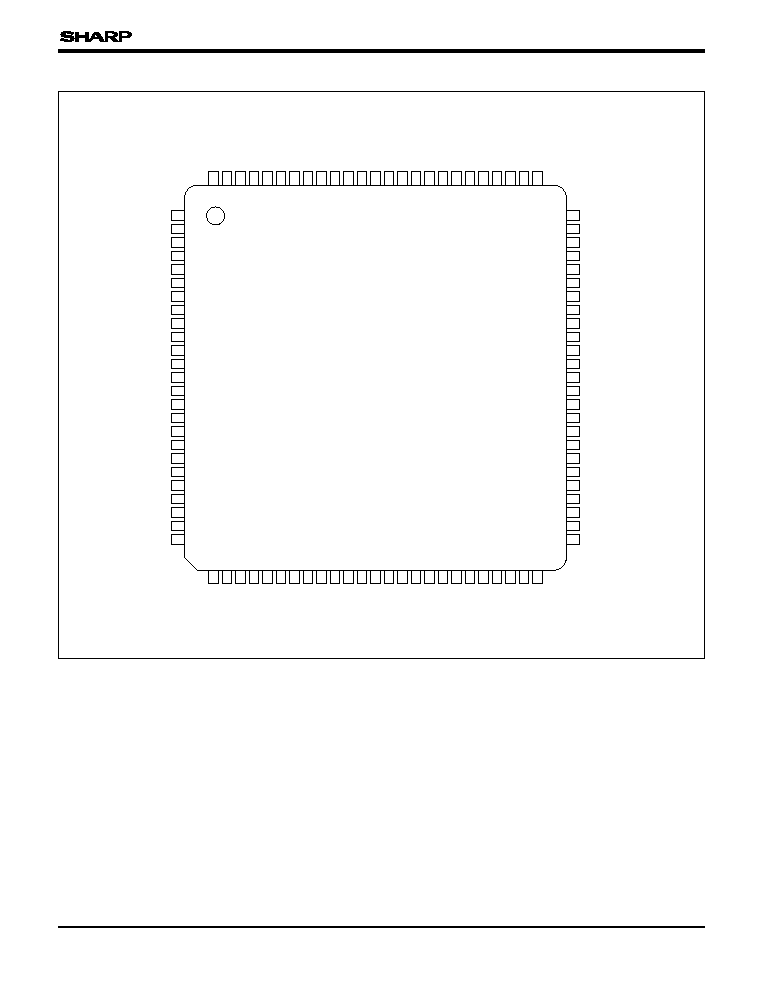
100-pin LQFP (LQFP100-P-1414) 0.5 mm pin-pitch
LR38266
LR38266
Digital Signal Processor for
Color CCD Cameras
LR38266
2
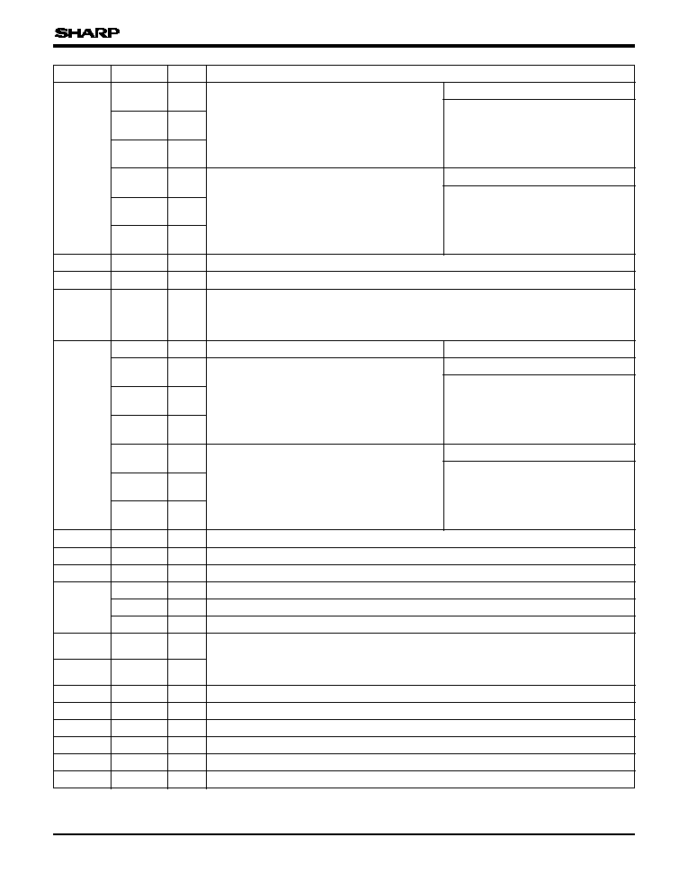
PIN CONNECTIONS
1
2
3
4
5
6
7
8
9
10
11
12
13
14
15
16
17
18
19
20
21
22
23
24
25
ACL
ADI
0
ADI
1
ADI
2
ADI
3
ADI
4
V
DD
GND
ADI
5
ADI
6
ADI
7
ADI
8
ADI
9
GND
V
DD
OCP
1
CSYN
GND
CKI
1
CKI
2
GND
CKI
0
GND
HP
VD
75
74
73
72
71
70
69
68
67
66
65
64
63
62
61
60
59
58
57
56
55
54
53
52
51
HD
1
DOC
EOO
V
DD
GND
DCK
1
YO
7
YO
6
YO
5
YO
4
GND
V
DD
YO
3
YO
2
YO
1
YO
0
V
REF
DA GND
DA V
DD
I
REF2
I
REF1
V
B2
V
B1
CENCO
YENCO
26
27
28
29
30
31
32
33
34
35
36
37
38
39
40
41
42
43
44
45
46
47
48
49
50
VRI
GND
FI
CBLK
CSYO
V
DD
GND
TST
1
TST
2
TST
3
TST
4
DCK
2
GND
CO
0
CO
1
CO
2
CO
3
GND
V
DD
CO
4
CO
5
CO
6
CO
7
TST
5
TST
6
100
99
98
97
96
95
94
93
92
91
90
89
88
87
86
85
84
83
82
81
80
79
78
77
76
DATA
7
DATA
6
DATA
5
DATA
4
DATA
3
DATA
2
DATA
1
DATA
0
GND
V
DD
MCO
1
ADD
6
ADD
5
ADD
4
ADD
3
ADD
2
ADD
1
ADD
0
V
DD
GND
SDI
SCK
SLDI
GND
ENC
100-PIN LQFP
TOP VIEW
(LQFP100-P-1414)
LR38266
3
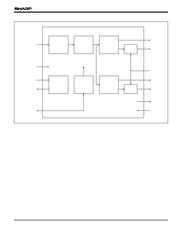
BLOCK DIAGRAM
ADI [9 : 0]
YOUT [7 : 0]
YENCO, VB
1
V
REF
COUT [7 : 0]
I
REF1
, I
REF2
CENCO, VB
2
DCK
1
, DCK
2
DOC
ADD [6 : 0]
DATA [7 : 0]
OBCP
SSG
DAC
DAC
1H, 2H
DELAY LINE
LUMINANCE
SIGNAL
PROCESS
COLOR
SIGNAL
PROCESS
MICRO-
COMPUTER
INTERFACE
CKI
0
, CKI
1
HP, CSYO, HD
1
CSYN, OCP
1
, VD, FI
CBLK, EOO, VRI
CKI
2
, ENC
SDI, SCK, SLDI
4
LR38266
PIN DESCRIPTION
PIN NO. SYMBOL
POLARITY
I/O
DESCRIPTION
1
ACL
ICU
All reset input. The internal circuit is initialized at power-on with a capacitor of
0.01 µF.
2
ADI
0
IC
ADI
0
to ADI
9
are digital signal inputs.
ADI
0
is LSB.
ADI
9
is MSB.
7
V
DD
≠
Supply of +3.3 V power.
IC
IC
IC
IC
ADI
1
ADI
2
ADI
3
ADI
4
3
4
5
6
A grounding pin.
≠
GND
18
Composite synchronous pulse output for analog video output.
O
CSYNC
17
Optical black clamp pulse output.
O
OCP
1
16
Supply of +3.3 V power.
≠
V
DD
15
A grounding pin.
≠
GND
14
IC
ADI
9
13
IC
ADI
8
12
IC
ADI
7
11
IC
ADI
6
10
ADI
0
to ADI
9
are digital signal inputs.
ADI
0
is LSB.
ADI
9
is MSB.
IC
ADI
5
9
A grounding pin.
≠
GND
8
19
CKI
1
IC
Clock input. The frequency is below for each CCD.
270 k, 410 k CCD : 14.31818 MHz
320 k, 470 k CCD : 14.1875 MHz
Clock input. The frequency is below for each CCD.
270 k CCD : 9.5454 MHz
320 k CCD : 9.4583 MHz
410 k CCD : 14.3181 MHz
470 k CCD : 14.1875 MHz
IC
CKI
2
20
22
CKI
0
IC
Clock input. The frequency is below for each CCD.
270 k, 410 k CCD : 28.6363 MHz
320 k, 470 k CCD : 28.3750 MHz
21
GND
≠
A grounding pin.
23
GND
≠
A grounding pin.
27
GND
≠
A grounding pin.
Vertical reset input. Built-in vertical counter is reset by a low-input of more than
one horizontal period.
ICS
VRI
26
Vertical drive pulse output.
O
VD
25
Horizontal drive pulse output.
O
HP
24
Composite synchronous pulse output.
Output timing is variable by output mode.
O
CSYO
30
Composite blanking pulse output.
O
CBLK
29
Supply of +3.3 V power.
≠
V
DD
31
Field index pulse output.
O
FI
28
32
GND
≠
A grounding pin.
5
LR38266
PIN NO. SYMBOL
POLARITY
I/O
DESCRIPTION
8-bit digital color signal output.
CO
0
is LSB.
CO
7
is MSB.
TO
CO
0
39
A grounding pin.
≠
GND
38
A grounding pin.
≠
GND
43
Clock output for digital C
OUT
.
O
DCK
2
37
Test input. Connected to low or open.
ICD
TST
4
36
Test input. Connected to low or open.
ICD
TST
3
35
Test input. Connected to low or open.
ICD
TST
2
34
Test input. Connected to low or open.
ICD
TST
1
33
40
41
42
CO
1
CO
2
CO
3
TO
TO
TO
52
CENCO
DAO
Analog C signal output.
51
YENCO
DAO
Analog Y signal output.
50
TST
6
ICD
Test input. Connected to low or open.
49
TST
5
ICD
Test input. Connected to low or open.
48
CO
7
TO
47
CO
6
TO
46
CO
5
TO
45
CO
4
TO
8-bit digital color signal output.
CO
0
is LSB.
CO
7
is MSB.
44
V
DD
≠
Supply of +3.3 V power.
Bias voltage output of built-in DA converter, connected to GND through a
capacitor.
DAO
V
B2
54
Bias voltage output of built-in DA converter, connected to GND through a
capacitor.
DAO
V
B1
53
57
DA V
DD
≠
Supply of +3.3 V power input for built-in DA converter.
56
I
REF2
DAO
Bias current output of built-in DA converter, connected to GND through a
resistor.
55
I
REF1
DAO
Bias current output of built-in DA converter, connected to GND through a
resistor.
Bias voltage input of built-in DA converter, connected to +1.0 V power supply.
DAI
V
REF
59
A grounding pin for built-in DA converter.
≠
DA GND
58
Supply of +3.3 V power.
≠
V
DD
64
Y digital outputs.
YO
0
is LSB.
YO
7
is MSB.
TO
YO
0
60
61
62
63
YO
1
YO
2
YO
3
TO
TO
TO
67
YO
5
TO
66
YO
4
TO
Y digital outputs.
YO
0
is LSB.
YO
7
is MSB.
65
GND
≠
A grounding pin.
68
YO
6
TO
TO
YO
7
69
6
LR38266
PIN NO. SYMBOL
POLARITY
I/O
DESCRIPTION
Control input of YO and CO. H level sets both YO and CO high-impedance.
ICD
DOC
74
Phase detector output comparing internal HD and HD
1
.
XTO
EOO
73
Clock input to encode color signal.
Internal Synchronous mode : CKI
2
Line Lock mode : same as CCD clock from outside or 4 f
SC
.
IC
ENC
76
Horizontal drive pulse generated from ENC (pin 76).
O
HD
1
75
A grounding pin.
≠
GND
77
Supply of +3.3 V power.
≠
V
DD
72
A grounding pin.
≠
GND
71
Clock output for YO output.
O
DCK
1
70
83
ADD
0
IC
Address input to select an output data of DATA pins used in auto white
balance and auto exposure.
For details, see
"Data Interface Timing"
.
82
V
DD
≠
Supply of +3.3 V power.
90
MCO
1
O
Control output to update internal data stored in DSP register. Data is updated
at the rising edge of MCO
1
.
81
GND
≠
A grounding pin.
80
SDI
IC
Timing pulse input to set SLDI data to DSP.
79
SCK
IC
Clock pulse input to set SLDI data to DSP.
78
SLDI
IC
Data input to set each coefficient of DSP.
IC
ADD
5
88
IC
ADD
4
87
IC
ADD
3
86
IC
ADD
2
85
IC
ADD
1
84
89
ADD
6
IC
A grounding pin.
≠
GND
92
Supply of +3.3 V power.
≠
V
DD
91
100 DATA
7
O
99
DATA
6
O
98
DATA
5
O
97
DATA
4
O
96
DATA
3
O
95
DATA
2
O
94
DATA
1
O
93
DATA
0
O
Data output to control auto white balance and auto exposure. Data of address
set by ADD inputs is output.
For details, see
"Data Interface Timing"
.
IC
: Input pin (CMOS level)
ICU
: Input pin (CMOS level with pull-up resistor)
ICD
: Input pin (CMOS level with pull-down resistor)
ICS
: Input pin (CMOS schmitt-trigger level with pull-
down resistor)
DAI
: Input pin for DA converter
O
: Output pin
TO
: Tri-state output pin
XTO
: Tri-state output pin
DAO
: DA converter output pin
7
LR38266
ADDRESS
BIT
CONTENTS
01h
6
Standby of DA converter
1 : Standby
Output format option
Output format option
Input data is delayed by 1 clock cycle
0 : Not delayed
1 : Delayed
CCD option
TV format option
0 : NTSC
1 : PAL
1
2
3
4
5
0
6
1
2
3
4
5
Image type option
0 : Normal
1 : Mirror
02h
Muting digital signal outputs
0 : OFF
1 : ON
Color killer function
0 : ON
1 : OFF
Horizontal edge enhancement
0 : ON
1 : OFF
Vertical edge enhancement
0 : ON
1 : OFF
The clock type to input the data
0 : Non-inverted
1 : Inverted
03h
8 bits
Position tuning of CSYNC with the range from +8 clock to ≠7 clock of CKI
1.
Upper 4 bits : CSYNC, Lower 4 bits : CSYO
0
The option of R/B sequence
0 : Normal
1
The option of U/V sequence
0 : Normal
2
Standby of delay lines
0 : OFF
1 : ON
4
Prohibited to change
0 : Should be kept as is
5
Set YL zero in color processing
0 : OFF
1 : ON
0
Standby of EOO function
0 : Standby
1
Interlace/Non-Interlace
0 : Interlace
2
The polarity of HG
0 : Normal
3
The polarity of SP1, SP2
0 : Normal
4
The polarity of EOO output
0 : Normal
04h
06h
08h
Position tuning of CBLK with the ditto range.
8 bits
NAME
STB_DA
TESYL
EX_SXB
INTL
HGCO
INVSP
EOOCTRL
MUTE_D
CKIL
APTHC
APTVC
ADTI2
ADTI1
MIR
TYPE1
TYPE2
TVMD
OUTPUT1
OUTPUT2
CBLKBALI
CSYNCVARI
SEL_RB
SEL_UV
RAM_ST
K1
CBK_Y
6
CBK_Y
7
The position tuning of Y-CBLK by CKI
2
clock
bit 7 = 0
bit 7 = 1
bit 6 = 0
No tune
≠1 clock
bit 6 = 1
1 clock
≠1 clock
MUTE_A
0
Muting analog signal outputs
0 : OFF
1 : ON
07h
bit 4 = 0
Y/C (bit 5 = 0) U/Y/V/Y (bit 5 = 1)
bit 4 = 1 Y, U/V (bit 5 = 0) Prohibited (bit 5 = 1)
bit 1 = 0 270 k/320 k with mirror Prohibited
bit 2 = 0
bit 2 = 1
CCD option
410 k/470 k
bit 1 = 1 270 k/320 k
BFVARI
1
The position tuning of color burst signal by
CKI
2
clock
bit 1 = 0
bit 1 = 1
bit 0 = 0
No tune
≠1 clock
bit 0 = 1
1 clock
≠1 clock
0
BFVARI
CBLK_UV
2
CBLK_UV
3
4
CBLK_C
5
CBLK_C
bit 5 = 0
bit 5 = 1
bit 4 = 0
No tune
≠1 clock
bit 4 = 1
1 clock
≠1 clock
bit 3 = 0
bit 3 = 1
bit 2 = 0
No tune
≠1 clock
bit 2 = 1
1 clock
≠1 clock
The position tuning of baseband C-CBLK by
CKI
2
clock
The position tuning of modulated C-CBLK by
CKI
2
clock
Not used
00h
INTERNAL COEFFICIENT TABLE
8
LR38266
ADDRESS
BIT
CONTENTS
NAME
11h
Coefficient to extract red color component
8 bits
CSP_R1
CB_R1
CB_R2
6 bits
8 bits
Coefficient of the black balance of red signal
(15h) MSB : sign, other 5 bits : upper 5 bits of coefficient
(16h) lower 8 bits of coefficient
15h
16h
CSP_B2
7 bits Coefficient to tune the base level of blue signal
14h
CSP_R2
7 bits Coefficient to tune the base level of red signal
13h
CSP_B1
8 bits Coefficient to extract blue color component
12h
19h
1Ah
Upper coefficient to make white balance of red signal
(19h) MSB of coefficient
(1Ah) lower 8 bits
1 bit
8 bits
WB_R1
WB_R2
17h
18h
Coefficient of the black balance of blue signal
(17h) MSB : sign, other 5 bits : upper 5 bits of coefficient
(18h) lower 8 bits of coefficient
6 bits
8 bits
CB_B1
CB_B2
WB_B1
WB_B2
1 bit
8 bits
Upper coefficient to make white balance of blue signal
(1Bh) MSB of coefficient
(1Ch) lower 8 bits
1Bh
1Ch
1Dh
Coefficient of R ≠ Y matrix
(MSB) sign bit
6 bits
MAT R ≠ Y
GA B ≠ Y 6 bits Coefficient of B ≠ Y gain
20h
BAS R ≠ Y
8 bits Coefficient of color burst level at R ≠ Y
(MSB) sign bit
22h
GA R ≠ Y
6 bits Coefficient of R ≠ Y gain
1Fh
MAT B ≠ Y 6 bits Coefficient of B ≠ Y matrix
(MSB) sign bit
1Eh
21h
The clock type of encoder input
0 : Non-Inverted 1 : Inverted
3
ENC_TI
L_fsc
MO_ENC
MUTE_E
2
1
0
Latched by fsc clock before encoding
0 : Latched
1 : Non-latched
Encoding phase of PAL
0 : 4 phases
1 : 16/5 phases
Muting color signal at encoder
0 : Normal
1 : Muting
26h
Positive range of white color signal at Q-axis
8 bits
WBA_QP
25h
Negative range of white color signal at I-axis
8 bits
WBA_IM
24h
Positive range of white color signal at I-axis
8 bits
WBA_IP
23h
Coefficient of color burst level at B ≠ Y
(MSB) sign bit
8 bits
BAS B ≠ Y
2Dh
Luminance level to suppress color signal
Upper 4 bits : higher luminance level
Lower 4 bits : lower luminance level
8 bits
CKI_HLGA
2Ch
Color suppression point at lower luminance level
8 bits
CKI_LCL
2Bh
Color suppression point at higher luminance level
8 bits
CKI_HCL
2Ah
Limiter of AWB function at lower luminance level
8 bits
WB_LCL
29h
Limiter of AWB function at higher luminance level
8 bits
WB_HCL
28h
Option of color signal type
I/Q or R ≠ Y/B ≠ Y
2 bits
WBA_SEL
27h
Negative range of white color signal at Q-axis
8 bits
WBA_QM
9
LR38266
ADDRESS
BIT
CONTENTS
NAME
2Eh
HT_SIG
6
Color killer timing at higher luminance
bit 6, bit 5, bit 4 000 : No tuning
2Fh
CKI_HECL
8 bits Horizontal aperture level to suppress color signal
001
1 clock cycle delay
010, 011
2 clock cycles delay
100, 101, 110
2 clock cycles advance
111
1 clock cycle advance
0
LT_0
bit 2, bit 1, bit 0 000 : No tuning
1
LT_1
Color killer timing at lower luminance
2
LT_SIG
4
HT_0
5
HT_1
001
1 clock cycle delay
010, 011
2 clock cycles delay
100, 101, 110
2 clock cycles advance
111
1 clock cycle advance
Vertical aperture level to suppress color signal
8 bits
CKI_VECL
30h
31h
CKI_EGA
8 bits
Aperture level to suppress color signal
Upper 4 bits : vertical aperture level
Lower 4 bits : horizontal aperture level
Level of edge signal
7
SEL_ESFT
32h
HET_0
0
HET_1
1
HET_SIG
2
VET_0
4
VET_1
5
VET_SIG
6
0 : 1/4 times
1 : 1 time
001
1 clock cycle delay
010, 011
2 clock cycles delay
100, 101, 110
2 clock cycles advance
111
1 clock cycle advance
bit 6, bit 5, bit 4 000 : No tuning
Color killer timing at vertical transient portion
Color killer timing at horizontal transient
portion
bit 2, bit 1, bit 0 000 : No tuning
001
1 clock cycle delay
010, 011
2 clock cycles delay
100, 101, 110
2 clock cycles advance
111
1 clock cycle advance
33h
CKI_LEV
5 bits Level to suppress color signal
Coring level of R ≠ Y signal
8 bits
NSUP_R ≠ Y
34h
39h
YL_AMP
8 bits YL signal level to make R ≠ Y and B ≠ Y
37h
YL_SFT1 2 bits Base level of YL signal
(37h) Upper 2 bits of coefficient
(38h) Lower 8 bits of coefficient
36h
8 bits
YL_SFT2
38h
1st input range of color gamma correction
8 bits
CGAM-A1
40h
C_NE1
2
The polarity of color signal
0 : Normal
1 : Inverted
C_NE2
1
The polarity of color signal at gamma output 0 : Normal
1 : Inverted
BLK_CTRL
0
CBLK availability at output
0 : ON
1 : OFF
Coring level of B ≠ Y signal
8 bits
NSUP_B ≠ Y
35h
4th input range of color gamma correction
8 bits
CGAM-A4
43h
3rd input range of color gamma correction
8 bits
CGAM-A3
42h
2nd input range of color gamma correction
8 bits
CGAM-A2
41h
5th input range of color gamma correction
8 bits
CGAM-A5
44h
LR38266
10
6th input range of color gamma correction
8 bits
CGAM-A6
45h
58h
CGAM-S5 8 bits Slope of 5th straight line at color gamma correction
57h
CGAM-S4 8 bits Slope of 4th straight line at color gamma correction
56h
CGAM-S3 8 bits Slope of 3rd straight line at color gamma correction
55h
CGAM-S2 8 bits Slope of 2nd straight line at color gamma correction
54h
CGAM-S1 8 bits Slope of 1st straight line at color gamma correction
53h
CGAM-F
1 bit
Polarity of color gamma correction
0 : +
1 : ≠
52h
CGAM-P10 8 bits Offset of 10th straight line at color gamma correction
51h
CGAM-P9 8 bits Offset of 9th straight line at color gamma correction
50h
CGAM-P8 8 bits Offset of 8th straight line at color gamma correction
4Fh
CGAM-P7 8 bits Offset of 7th straight line at color gamma correction
4Eh
CGAM-P6 8 bits Offset of 6th straight line at color gamma correction
4Dh
CGAM-P5 8 bits Offset of 5th straight line at color gamma correction
4Ch
CGAM-P4 8 bits Offset of 4th straight line at color gamma correction
4Bh
CGAM-P3 8 bits Offset of 3rd straight line at color gamma correction
4Ah
CGAM-P2 8 bits Offset of 2nd straight line at color gamma correction
49h
CGAM-P1 8 bits Offset of 1st straight line at color gamma correction
48h
CGAM-A9 8 bits 9th input range of color gamma correction
47h
CGAM-A8 8 bits 8th input range of color gamma correction
46h
CGAM-A7 8 bits 7th input range of color gamma correction
Slope of 7th straight line at color gamma correction
8 bits
CGAM-S7
5Ah
Slope of 6th straight line at color gamma correction
8 bits
CGAM-S6
59h
ADDRESS
BIT
CONTENTS
NAME
Slope of 10th straight line at color gamma correction
8 bits
CGAM-S10
5Dh
Slope of 9th straight line at color gamma correction
8 bits
CGAM-S9
5Ch
Slope of 8th straight line at color gamma correction
8 bits
CGAM-S8
5Bh
67h
6ADV
4
1 : 6 clocks advance of luminance signal
0 : No variation
66h
VARI_MASK 4 bits Position to erase color signal by luminance mask signal
65h
Not used
64h
APT_VCL
7 bits Coring level of vertical aperture signal
63h
APT_VGA
5 bits Vertical aperture gain
62h
APT_HCL
7 bits Coring level of horizontal aperture signal
61h
APT_HGA 5 bits Horizontal aperture gain
60h
SETUP
6 bits Set up level of luminance signal
1 : 1 clock delay of luminance signal
0 : No variation
0
1DLY
1 : 2 clocks delay of luminance signal
0 : No variation
1
2DLY
1 : 4 clocks delay of luminance signal
0 : No variation
2
4DLY
1 : 8 clocks advance of luminance signal
0 : No variation
3
8ADV
68h
HVARI
2 bits Position of horizontal aperture signal
11
LR38266
ADDRESS
BIT
CONTENTS
NAME
6Ah
Y_NESFT
8 bits Base level of luminance signal
7th input range of color gamma correction
8 bits
CGAM-A7
76h
6th input range of color gamma correction
8 bits
CGAM-A6
75h
5th input range of color gamma correction
8 bits
CGAM-A5
74h
4th input range of color gamma correction
8 bits
CGAM-A4
73h
3rd input range of color gamma correction
8 bits
CGAM-A3
72h
2nd input range of color gamma correction
8 bits
CGAM-A2
71h
1st input range of color gamma correction
8 bits
CGAM-A1
70h
Not used
6Fh
Not used
6Eh
Not used
6Dh
Masking level of luminance signal
8 bits
MASK_NE
6Ch
Luminance signal level
8 bits
Y_NEAMP
6Bh
9th input range of color gamma correction
8 bits
CGAM-A9
78h
8th input range of color gamma correction
8 bits
CGAM-A8
77h
82h
CGAM-P10 8 bits Offset of 10th straight line at color gamma correction
81h
CGAM-P9 8 bits Offset of 9th straight line at color gamma correction
80h
CGAM-P8 8 bits Offset of 8th straight line at color gamma correction
7Fh
CGAM-P7 8 bits Offset of 7th straight line at color gamma correction
7Eh
CGAM-P6 8 bits Offset of 6th straight line at color gamma correction
7Dh
CGAM-P5 8 bits Offset of 5th straight line at color gamma correction
7Ch
CGAM-P4 8 bits Offset of 4th straight line at color gamma correction
7Bh
CGAM-P3 8 bits Offset of 3rd straight line at color gamma correction
7Ah
CGAM-P2 8 bits Offset of 2nd straight line at color gamma correction
79h
CGAM-P1 8 bits Offset of 1st straight line at color gamma correction
Slope of 4th straight line at color gamma correction
8 bits
CGAM-S4
87h
Slope of 3rd straight line at color gamma correction
8 bits
CGAM-S3
86h
Slope of 2nd straight line at color gamma correction
8 bits
CGAM-S2
85h
Slope of 1st straight line at color gamma correction
8 bits
CGAM-S1
84h
Polarity of color gamma correction
0 : +
1 : ≠
1 bit
CGAM-F
83h
The polarity of luminance signal
0 : Normal
1 : Inverted
0
Y_NEGA
Pedestal level of luminance signal
0 : 16th step
1 : 0 step
1
SEL_BLK
CBLK availability for luminance signal
0 : ON
1 : OFF
2
CBLK_OFF
Muting analog luminance signal output
0 : Normal
1 : Muting
3
Y_MUTE
69h
Slope of 8th straight line at color gamma correction
8 bits
CGAM-S8
8Bh
Slope of 7th straight line at color gamma correction
8 bits
CGAM-S7
8Ah
Slope of 6th straight line at color gamma correction
8 bits
CGAM-S6
89h
Slope of 5th straight line at color gamma correction
8 bits
CGAM-S5
88h
Slope of 10th straight line at color gamma correction
8 bits
CGAM-S10
8Dh
Slope of 9th straight line at color gamma correction
8 bits
CGAM-S9
8Ch
8Eh
Not used
12
LR38266
ADDRESS
BIT
CONTENTS
NAME
8Fh
Not used
The option of white balance data equation
0 : Accumulated data/Image area
1 : Accumulated data/Number of data
7
SEL_WBD
A0h
I_WBA_H
3
The area in horizontal to detect average level to control both the exposure and
white balance
0 : OFF
1 : ON
PEAKA_V
4
The area in vertical to detect peak level to control the exposure
0 : OFF
1 : ON
PEAHA_H
5
The area in horizontal to detect peak level to control the exposure
0 : OFF
1 : ON
PEAK4_8
6
The option to detect peak level to control the exposure
0 : Accumulated data of 4 pixels
1 : Accumulated data of 8 pixels
The area in vertical to detect average level to control both the exposure and
white balance
0 : OFF
1 : ON
2
I_WBA_V
MASK_V
0
Vertical mask signal availability
0 : OFF
1 : ON
MASK_H
1
Horizontal mask signal availability
0 : OFF
1 : ON
Lower 8 bits of ending point to mask in vertical
8 bits
VMSKR_L
Upper 1 bit of ending point to mask in vertical
1 bit
VMSKR_U
Lower 8 bits of starting point to mask in vertical
8 bits
VMSKF_L
Upper 1 bit of starting point to mask in vertical
1 bit
VMSKF_U
Lower 8 bits of ending point to mask in horizontal
8 bits
HMSKR_L
Upper 2 bits of ending point to mask in horizontal
2 bits
HMSKR_U
Lower 8 bits of starting point to mask in horizontal
8 bits
HMSKF_L
Upper 2 bits of starting point to mask in horizontal
2 bits
HMSKF_U
A1h
A9h
A8h
A7h
A5h
A4h
A3h
A2h
13
LR38266
OUTPUT DATA
Output Data Table
ADDRESS
BIT
CONTENTS
NAME
Average data to control exposure
8 bits
IRIS-1-1 to 8
00 to 07h
30 to 37h IRIS-7-1 to 8 8 bits Average data to control exposure
28 to 2Fh IRIS-6-1 to 8 8 bits Average data to control exposure
20 to 27h IRIS-5-1 to 8 8 bits Average data to control exposure
18 to 1Fh IRIS-4-1 to 8 8 bits Average data to control exposure
10 to 17h IRIS-3-1 to 8 8 bits Average data to control exposure
08 to 0Fh IRIS-2-1 to 8 8 bits Average data to control exposure
8 bits
AWBQ-2-1 to 4
54 to 57h
8 bits
AWBI-4-1 to 4
4C to 4Fh
Average data of Q/B ≠ Y axis to control auto white balance
Average data of I/R ≠ Y axis to control auto white balance
8 bits
AWBI-3-1 to 4
48 to 4Bh
Average data of I/R ≠ Y axis to control auto white balance
8 bits
AWBI-2-1 to 4
44 to 47h
8 bits
AWBI-1-1 to 4
40 to 43h
Average data to control exposure
8 bits
IRIS-8-1 to 8
38 to 3Fh
50 to 53h AWBQ-1-1 to 4 8 bits
8 bits
AWBQ-4-1 to 4
5C to 5Fh
8 bits
AWBQ-3-1 to 4
58 to 5Bh
Average data of Q/B ≠ Y axis to control auto white balance
8 bits
C3_OB_B
64h
8 bits
C1_OB_R
63h
8 bits
OB_DATA
62h
Average data of optical pixels for Mg + Cy
8 bits
L_PEAK
61h
Average data of optical pixels for Mg + Ye
8 bits
H_PEAK
60h
Average data of optical pixels
Minimum luminance signal out of 64 blocks
Maximum luminance signal out of 64 blocks
LR38266
14
Position of Each Output on Image Screen
(1) Luminance Signal Data to Control Exposure
Left-top Side of Image
(2) Color Signal Data to Control Auto White Balance
Left-top Side of Image
IRIS-1-1
IRIS-8-1
IRIS-7-1
IRIS-6-1
IRIS-5-1
IRIS-4-1
IRIS-3-1
IRIS-2-1
IRIS-2-8
IRIS-3-8
IRIS-4-8
IRIS-5-8
IRIS-6-8
IRIS-7-8
IRIS-8-8
IRIS-1-8
IRIS-2-7
IRIS-3-7
IRIS-4-7
IRIS-5-7
IRIS-6-7
IRIS-7-7
IRIS-8-7
IRIS-1-7
IRIS-2-6
IRIS-3-6
IRIS-4-6
IRIS-5-6
IRIS-6-6
IRIS-7-6
IRIS-8-6
IRIS-1-6
IRIS-2-5
IRIS-3-5
IRIS-4-5
IRIS-5-5
IRIS-6-5
IRIS-7-5
IRIS-8-5
IRIS-1-5
IRIS-2-4
IRIS-3-4
IRIS-4-4
IRIS-5-4
IRIS-6-4
IRIS-7-4
IRIS-8-4
IRIS-1-4
IRIS-2-3
IRIS-3-3
IRIS-4-3
IRIS-5-3
IRIS-6-3
IRIS-7-3
IRIS-8-3
IRIS-1-3
IRIS-2-2
IRIS-3-2
IRIS-4-2
IRIS-5-2
IRIS-6-2
IRIS-7-2
IRIS-8-2
IRIS-1-2
AWBI/AWBQ-1-1
AWBI/AWBQ-4-1
AWBI/AWBQ-3-1
AWBI/AWBQ-2-1
AWBI/AWBQ-2-2
AWBI/AWBQ-3-2
AWBI/AWBQ-4-2
AWBI/AWBQ-1-2
AWBI/AWBQ-2-2
AWBI/AWBQ-3-2
AWBI/AWBQ-4-2
AWBI/AWBQ-1-2
AWBI/AWBQ-2-2
AWBI/AWBQ-3-2
AWBI/AWBQ-4-2
AWBI/AWBQ-1-2
Either I or R ≠ Y is selectable by address 28h.
Either Q or B ≠ Y is selectable by address 28h.
LR38266
15
ABSOLUTE MAXIMUM RATINGS
RECOMMENDED OPERATING CONDITIONS
PARAMETER
SYMBOL
Power supply voltage
V
DD
Input voltage
V
I
ELECTRICAL CHARACTERISTICS
(V
DD
= 3.3±0.33 V, T
OPR
= ≠20 to +70 ∞C)
Input "Low" voltage
V
IL
Input "High" voltage
V
IH
Input "Low" voltage
V
T≠
V
T+
Hysteresis voltage
V
T+
≠ V
T≠
Output "Low" voltage
V
OL1
Output leakage current
|I
OZ
|
Output "Low" voltage
V
OL1
Output "High" voltage
V
OH2
Input "High" current
|I
OH2
|
Output "Low" voltage
V
OL1
Output "High" voltage
V
OH2
Resolution
RES
Linearity error
EL
Differential error
ED
Full scale current
|I
FS
|
Reference voltage
V
REF
Reference resistance
R
REF
Output load resistance
R
OUT
PARAMETER
SYMBOL
CONDITIONS
Input "High" voltage
V
OH2
Output "High" voltage
MIN.
0.8V
DD
0.8V
DD
0.9V
DD
0.9V
DD
≠1.0
0.9V
DD
0.2
4.8
75
10
8
13
TYP.
1.0
MAX.
0.2V
DD
0.2V
DD
±1.0
±3.0
0.1V
DD
0.1V
DD
1.0
0.1V
DD
V
REF
= 1.0 V
R
REF
= 4.8 k$
R
OUT
= 75 $
I
OH
= 0.8 mA
I
OL
= ≠1.6 mA
V
IN
= V
DD
I
OH
= 0.8 mA
I
OL
= ≠1.6 mA
High-impedance
I
OH
= 0.8 mA
I
OL
= ≠1.6 mA
$
V
V
V
µA
V
V
µA
V
V
Bit
LSB
LSB
mA
V
V
V
V
V
UNIT
k$
NOTE
2
1
6
3
4
µA
µA
High-impedance
V
IN
= 0 V
1.0
10
≠1.0
|I
OL1
|
Input "Low" current
|I
OZ
|
Output leakage current
≠0.3 to V
DD
+ 0.3
≠0.3 to +4.6
RATING
UNIT
V
V
∞C
≠55 to +150
T
STG
Storage temperature
V
≠0.3 to V
DD
+ 0.3
V
O
Output voltage
PARAMETER
SYMBOL
Power supply voltage
V
DD
Operating temperature
T
OPR
≠20
3.0
MIN.
UNIT
V
∞C
MHz
f
CK
Input clock frequency
28.6
TYP.
MAX.
3.3
3.6
+25
+70
5
7
9
8
8
10
NOTES :
1. Applied to inputs (IC, ICD, ICU).
2. Applied to input (ICS).
3. Applied to output (TO).
4. Applied to output (XTO).
5. Applied to input (ICU).
6. Applied to input (ICD).
7. Applied to output (O).
8. Applied to outputs (YENCO, CENCO).
9. Applied to input (V
REF
).
10. Applied to inputs (I
REF1
, I
REF2
).
LR38266
16
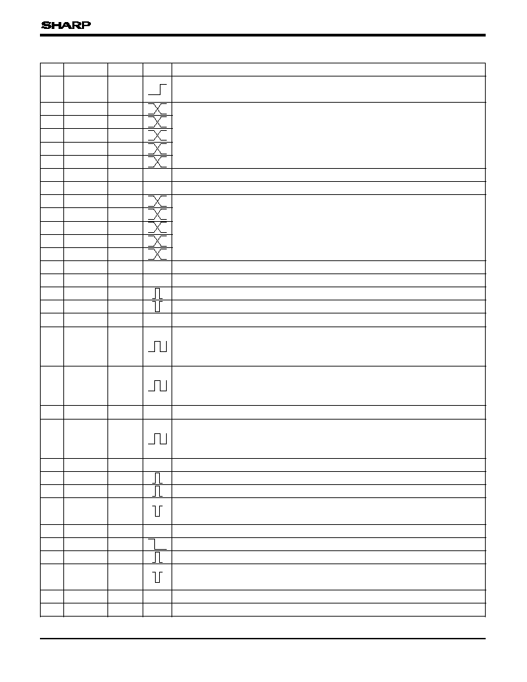
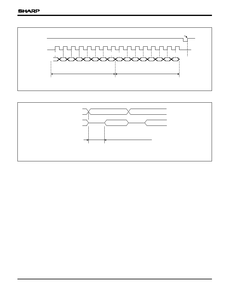
Data Interface Timing
Data Output
Data Input
SCK
SDI
SLDI
Address
SCK should be slower than 20 MHz.
Data
A
7
A
6
A
5
A
4
A
3
A
2
A
1
A
0
D
7
D
6
D
5
D
4
D
3
D
2
D
1
D
0
Data is stored in LR38266
LSB MSB
LSB
MSB
Data output in 47 ns or more after address input is valid.
ADD [6 : 0]
DATA [7 : 0]
MAX. 47 ns

17
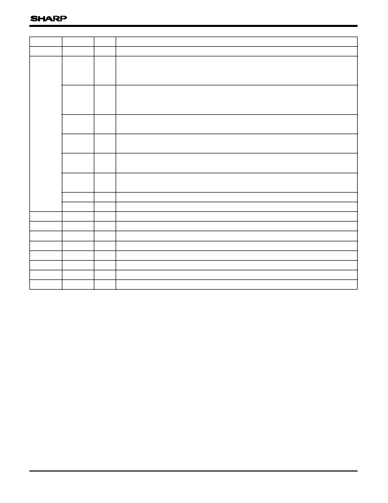
DETAIL EXPLANATION
CCD
CCD type out of 270 k, 320 k, 410 k and 470 k
pixels is selected by address 01h.
Output Signal Format
(1) Analog Video Signal Output
Built-in DA converters output luminance (Y) signal
without CSYNC and modulated color signal of
NTSC or PAL.
Standby mode of DA converter makes DA output
pins high impedance.
(2) Digital Video Signal Output (address 01h)
One out of three formats below is selectable by
address 01h. High level of pin 74 as DOC makes
all digital output pins high impedance.
1. 8-bit Y and 8-bit C
2. 8-bit Y and 8-bit U/V
3. 8-bit U/Y/V/Y
Camera Control Data Output
(1) Exposure Control Data Output (64 data with 8
bits and 2 data with 8 bits)
The user-defined image area consists of 64 blocks
divided into 8 x 8 blocks. Each average luminance
level is output to DATA output pins by setting ADD
input pins.
In the defined area, the maximum luminance level
and the minimum luminance level are output to
DATA output pins.
(2) White Balance Control Data Output (two kinds
of 16 data with 8 bits)
The user-defined image area consists of 16 blocks
divided into 4 x 4 blocks. Average color signal
levels of either both I and Q or both R ≠ Y and B
≠ Y are output to DATA output pins by setting ADD
input pins.
(3) Black Balance Control Data Output (3 data with
8 bits)
Three kinds of outputs below are at DATA output
pins.
∑ An average signal of CCD optical black portion
consisting of 4 pixels per horizontal line for 128
horizontal lines located in the image center.
∑ An average signal of CCD optical black portion
consisting of 2 pixels per horizontal line for 128
horizontal lines located in the image center, which
is available to tune the base level of Mg + Ye
color signal component.
∑ An average signal of CCD optical black portion
consisting of 2 pixels per horizontal line for 128
horizontal lines located in the image center, which
is available to tune the base level of Mg + Cy
color signal component.
Camera Signal Processing
(1) Optical Black Signal Clamping
The optical black signal portion is clamped so as to
be 64h by using the average level of the input
digital signal. The averaging is done for every field.
(2) Horizontal Period Delay Line
There are two horizontal delay lines in this IC for
camera signal processing.
(3) Digital Filter for Luminance Signal
These are low-pass filters to make a Y signal from
the color CCD signal.
(4) Gamma Correction for Luminance Signal
10-bit input signal is converted into an 8-bit signal
with a gamma curve defined by 10 straight lines.
Slope and position of every straight line can be set
by address.
(5) Edge Enhancement of Luminance Signal
After gamma correction, the edge of the luminance
signal is enhanced in both horizontal and vertical.
How to enhance is tunable by address.
LR38266

18
(6) Set-up Level of Luminance Signal
The set-up level is tunable by address.
(7) Polarity Option and Level Tuning of Luminance
Signal
The polarity of the input signal from the AD
converter can be inverted before filtering.
The DC offset level and the amplitude are tunable
by address.
(8) Masking Luminance Signal
The restricted area in the whole image can be set
by address.
The exposure function and the auto white balance
function can be used only in the restricted area.
(9) Extract of Color Signal Component
Color signal components are extracted by following
processing calculation.
Red = (Mg + Ye) ≠ K
1
(G + Cy)
Blue = (Mg + Cy) ≠ K
2
(G + Ye)
YL = ((Mg + Ye) + (G + Cy) + (Mg + Cy) + (G + Ye))/4
K
1
and K
2
are variable by address.
(10) Digital Filter of Color Signal Component
Red, blue and YL are passed to limit each
bandwidth so as to be half of extracted signals by
low-pass filters.
(11) Black Level Clamping of Color Signal Component
The black level of red and blue signals can be
tuned by address 15h, 16h, 17h, and 18h.
(12) White Balance
The amplitude of red and blue signals can be tuned
by address 19h, 1Ah, 1Bh, and 1Ch for white
balance situation.
(13) Color Gamma Correction
10-bit input signal of red, blue and YL signals are
converted into an 8-bit signal with gamma curve
defined by 10 straight lines.
The slope and position of every straight line can be
set by address.
(14) Color Matrix Correction
Color rendition can be tuned by address 1Dh and
1Eh under below equation.
R ≠ Y = (R ≠ Y) + K
1
(B ≠ Y)
B ≠ Y = (B ≠ Y) + K
2
(R ≠ Y)
(15) Color Level Adjustment
The amplitude of R ≠ Y and B ≠ Y can be tuned
by address 1Fh and 20h.
(16) Color Level Suppression
A false color signal at both the transient portion of
luminance signal and the high-light portion of
luminance signal can be suppressed by address
2Bh, 2Ch, 2Dh, 2Eh, 30h, 31h, 32h, 33h, 34h and
35h.
(17) Polarity Option and Level Tuning of Color Signal
The polarity of the color component signal can be
inverted before gamma correction.
The DC offset level and the amplitude are tunable
by address 36h, 37h, 38h and 39h.
(18) NTSC/PAL Color Signal Encoder
R ≠ Y and B ≠ Y color signals are modulated
under NTSC or PAL format.
Modulated clock frequency and TV format are
selected by address 03h, 21h, 22h and 23h.
Line-lock system requires the clock generator
outside LR38266.
(19) Accumulator to Control Exposure
Three kinds of output data below become available
by address A0h, 00h to 3Fh, 60h and 61h.
∑ Average signal in either the whole image or
restricted area.
∑ Maximum signal in either the whole image or
restricted area.
∑ Minimum signal in either the whole image or
restricted area.
LR38266
(20) Accumulator to Control White Balance
Output data below become available by address
24h, 25h, 26h, 27h, 28h, 29h, 2Ah, A0h and 4Fh to
5Fh.
Average signal of I (R ≠ Y) and Q (B ≠ Y) in 16
areas of the whole image.
These data can be weighted by both the color
zone of I-axis and/or Q-axis and the range of
luminance.
(21) Accumulator to Control Color Black Balance
Average signal of the optical black portion to clamp
the black level of color signal is available by
address 62h, 63h and 64h.
(22) Others
∑ The output timing of synchronous signals are
available by address 06h, 07h and 08h.
∑ Functions like standby, muting, etc. are available
by address 01h, 03h, 04h and 21h.
LR38266
19
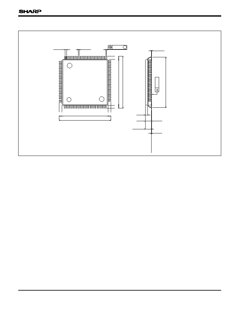
PACKAGES FOR CCD AND CMOS DEVICES
20
Unit : mm
0.1
±0.1
Package
base plane
1
0.125
±0.05
0.2
±0.08
0.5
TYP.
25
26
50
51
75
76
100
14.0
±0.2
14.0
±0.2
16.0
±0.3
1.4
±0.2
0.6375
15.0
±0.2
(1.0)
(1.0)
(1.0 )
(1.0)
0.08
0.1
M
16.0
±0.3
1.70
MAX.
100 LQFP (LQFP100-P-1414)
PACKAGE
(Unit : mm)