 | –≠–ª–µ–∫—Ç—Ä–æ–Ω–Ω—ã–π –∫–æ–º–ø–æ–Ω–µ–Ω—Ç: LR38581 | –°–∫–∞—á–∞—Ç—å:  PDF PDF  ZIP ZIP |
DESCRIPTION
The LR38581 is a CMOS timing generator IC which
generates timing pulses for driving 270 k/320 k-
pixel color CCD area sensors with a dual-power-
supply operation and processing pulses for color
video signals.
FEATURES
∑ Designed for 270 k/320 k-pixel color CCD area
sensors with a dual-power-supply-operation
∑ Switchable between NTSC and PAL modes
∑ Switchable between normal and mirror images
∑ Level shifter for readout and shutter pulses included
∑ +3.3 V, +5 V and +12.5 V power supplies
∑ Package :
48-pin QFP (QFP048-P-0707) 0.5 mm pin-pitch
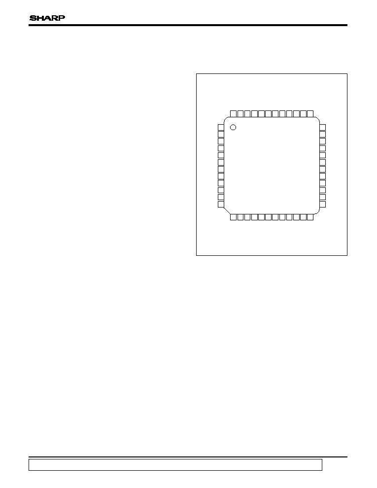
PIN CONNECTIONS
LR38581
In the absence of confirmation by device specification sheets, SHARP takes no responsibility for any defects that may occur in equipment using any SHARP devices shown in
catalogs, data books, etc. Contact SHARP in order to obtain the latest device specification sheets before using any SHARP device.
1
LR38581
Timing Generator IC for 270 k/320 k-pixel
Color CCDs with Dual-power-supply Operation
1
48 47 46 45 44 43 42 41 40 39
37
13 14 15 16 17 18 19 20 21 22 23 24
2
3
4
5
6
7
8
9
10
11
12
36
35
34
33
32
31
30
29
28
27
26
25
OBCP
CLP
PBLK
FS
FCDS
RS
GND
V
DD3
ED
0
ED
1
ED
2
MIR
SAD
2
SAD
1
HP
VD
ADCK
GND
V
DD3
CDCK
SGCK
GND
CKO
CKI
TST
1
TST
2
V
DD5
V
1
V
2
V
3
V
4
NC
GND
VTG
V
DD12
OFD
GND
FH
2B
FH
2
FH
1
V
DD5
GND
FH
1B
FR
TVMD
PLCH
TST
4
38
TST
3
48-PIN QFP
TOP VIEW
(QFP048-P-0707)
LR38581
2
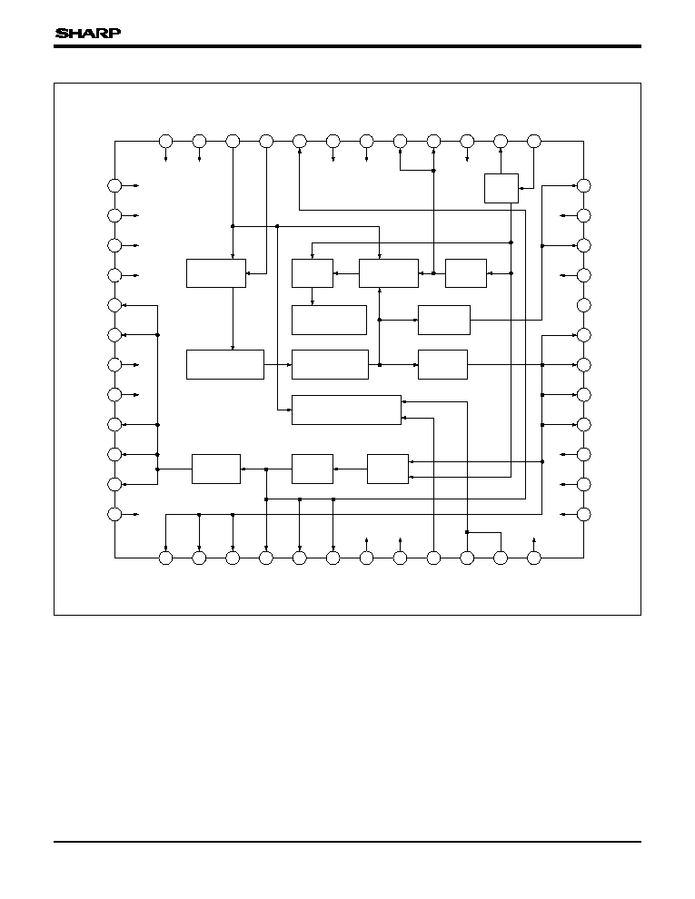
BLOCK DIAGRAM
DECODER
& LATCH
SAD
2
SAD
1
HP
VD
ADCK
GND
V
DD3
CDCK
SGCK
GND
CKO
CKI
36
35
34
33
32
31
30
29
28
27
26
25
OFD
V
DD12
VTG
GND
NC
V
4
V
2
V
3
V
1
V
DD5
TST
2
TST
1
OBCP
CLP
PBLK
FS
FCDS
RS
GND
V
DD3
ED
1
ED
0
ED
2
MIR
TST
3
TST
4
PLCH
TVMD
FR
FH
1B
GND
V
DD5
FH
1
FH
2
FH
2B
GND
MIX
1/3
H COUNTER
LEVEL
SHIFTER
(12.5 V)
1/4
1/2
PRESET
RESET
OSC
13
14
15
16
17
18
19
20
21
22
23
24
1
2
3
4
5
6
7
8
9
10
11
12
48
47
46
45
44
43
42
41
40
39
38
37
V COUNTER
SHUTTER CONTROL
LEVEL
SHIFTER
LEVEL
SHIFTER

LR38581
3
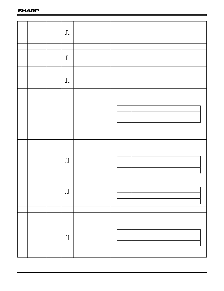
PIN DESCRIPTION
PIN NO. SYMBOL
I/O
POLARITY
PIN NAME
DESCRIPTION
1
OBCP
O4MA3
Optical black clamp
pulse output
A pulse to clamp the optical black signal. This pulse stays
low during the absence of effective pixels within the vertical
blanking. The polarity can be changed by PLCH (pin 39).
2
CLP
O4MA3
AD input signal
clamp pulse output
A pulse to clamp the AD input signal. The polarity can
be changed by PLCH (pin 39).
3
PBLK
O4MA3
Pre-blanking pulse
output
A pulse that corresponds to the cease period of the
horizontal transfer pulse.
4
FS
O4MA32
CDS pulse output 1
A pulse to sample-hold the signal from CCD.
The polarity can be changed by PLCH (pin 39).
The output phase of FS is selected by serial data.
5
FCDS
O4MA32
CDS pulse output 2
A pulse to clamp the feed-through level from CCD.
The polarity can be changed by PLCH (pin 39).
The output phase of FCDS is selected by serial data.
6
RS
O4MA32
S/H pulse output
A pulse to sample-hold the signal from CDS circuit.
The polarity can be changed by PLCH (pin 39).
The output phase of RS is selected by serial data.
A grounding pin.
Ground
≠
GND
7
≠
≠
9
ED
0
ICSU3
Shift register clock
input
An input pin for the clock of the shift register, to control
the functions of LR38581. For details, see
"Serial Data
Control."
≠
8
V
DD3
≠
Power supply
Supply of +3.3 V power.
An input pin for the data of the shift register, to control
the functions of LR38581. For details, see
"Serial Data
Control."
Shift register data
input
ICSU3
ED
1
10
≠
≠
11
ED
2
ICSU3
Strobe pulse input
An input pin for the strobe pulse, to control the functions
of LR38581. For details, see
"Serial Data Control."
An input pin to select mirror or normal image mode
L level
: Normal image mode
H level or open
: Mirror image mode
Mirror mode
selection
ICU3
MIR
12
≠
MIR
FH
1B
FH
2B
L (Normal mode)
FH
1
FH
2
FH
1
FH
2
H or open (Mirror mode)
≠
13
TST
1
ICD5
Test pin 1
A test pin. Set open or to L level in the normal mode.
A test pin. Set open or to L level in the normal mode.
Test pin 2
ICD5
TST
2
14
≠
≠
15
V
DD5
≠
Power supply
Supply of +5 V power.
16
V
1
O4MA52
Vertical transfer
pulse output 1
A pulse to drive vertical CCD shift register.
Connect to ÿ
V1
pin of CCD.
A pulse to drive vertical CCD shift register.
Connect to ÿ
V3
pin of CCD.
Vertical transfer
pulse output 3
O4MA52
V
3
18
A pulse to drive vertical CCD shift register.
Connect to ÿ
V2
pin of CCD.
Vertical transfer
pulse output 2
O4MA52
V
2
17
LR38581
4
PIN NO. SYMBOL
I/O
POLARITY
PIN NAME
DESCRIPTION
A pulse to drive vertical CCD shift register.
Connect to ÿ
V4
pin of CCD.
Vertical transfer
pulse output 4
O4MA52
V
4
19
20
NC
≠
No connection
No connection
≠
≠
A grounding pin.
Ground
≠
GND
21
≠
Supply of +12.5 V power.
Power supply
≠
V
DD12
23
22
VTG
O12MHV
Readout pulse
output
A pulse that transfers the charge of the photo-diode to
the vertical shift register.
Connect to VTG pin of CCD.
24
OFD
O12MHV
OFD pulse output
A pulse that sweeps the charge of the photo-diode
for electronic shutter. Connect to OFD pin of CCD.
Held at L level at normal mode.
An input pin for reference clock oscillation.
Connect to CKO (pin 26) with R.
The frequencies are as follows :
fH = Horizontal frequency
Clock input
OSCI3
CKI
25
≠
TVMD
L
H
28.37500 MHz (1816 fH)
28.63636 MHz (1820 fH)
Frequency
≠
26
CKO
OSCO3
Clock output
An output pin for reference clock oscillation.
The output is the inverse of CKI (pin 25).
A grounding pin.
Ground
≠
GND
27
≠
28
SGCK
O4MA32
SSG clock output
An output pin to generate HP and VD pulses.
The frequencies are as follows :
An output pin for DSP IC.
The frequencies are as follows :
DSP clock output
O4MA32
CDCK
29
TVMD
L
H
9.4375 MHz (1816/3 fH)
9.5035 MHz (1820/3 fH)
Frequency
≠
30
V
DD3
≠
Power supply
Supply of +3.3 V power.
A grounding pin.
Ground
≠
GND
31
≠
32
ADCK
O4MA32
AD clock output
An output pin for AD converter.
The frequencies are as follows :
The output phase of ADCK is selected by SAD
1
(pin 35)
and SAD
2
(pin 36).
TVMD
L
H
9.4375 MHz (1816/3 fH)
9.5035 MHz (1820/3 fH)
Frequency
TVMD
L
H
14.18750 MHz (908 fH)
14.31818 MHz (910 fH)
Frequency
LR38581
5
PIN NO. SYMBOL
I/O
POLARITY
PIN NAME
DESCRIPTION
35
SAD
1
ICU3
ADCK phase control
input 1
An input pin to select the phase of ADCK.
34
HP
IC3
Horizontal reference
pulse input
An input pin for reference of horizontal pulse.
Connect to HD pin of DSP IC.
37
TST
3
ICD5
Test pin 3
A test pin. Set open or to L level in the normal mode.
≠
SAD
1
SAD
2
Phase
60∞ delay
L
H or open
0∞
L
L
H or open
H or open
240∞ delay
L
H or open
180∞ delay
≠
ADCK phase control
input 2
ICU3
SAD
2
36
≠
≠
An input pin to select TV standards.
L level
: NTSC mode
H level or open
: PAL mode
TV mode selection
input
ICU5
TVMD
40
≠
A grounding pin.
Ground
≠
GND
43
≠
An input pin to select the polarity of OBCP (pin 1),
CLP (pin 2), FS (pin 4), FCDS (pin 5) and RS (pin 6).
Polarity selection
input
ICU5
PLCH
39
≠
A test pin. Set open or to L level in the normal mode.
Test pin 4
ICD5
TST
4
38
41
FR
O4MA53
Reset pulse output
A pulse to reset the charge of output circuit.
Connect to ÿ
R
pin of CCD through the DC offset circuit.
The output phase of FR is selected by serial data.
42
FH
1B
O4MA52
Horizontal transfer
pulse output 1B
A pulse to drive horizontal CCD shift register.
Connect to ÿ
H1B
pin of CCD.
45
FH
1
O4MA53
Horizontal transfer
pulse output 1
A pulse to drive horizontal CCD shift register.
Connect to ÿ
H1
pin of CCD.
44
V
DD5
≠
Power supply
Supply of +5 V power.
≠
A pulse to drive horizontal CCD shift register.
Connect to ÿ
H2B
pin of CCD.
Horizontal transfer
pulse output 2B
O4MA52
FH
2B
47
A pulse to drive horizontal CCD shift register.
Connect to ÿ
H2
pin of CCD.
Horizontal transfer
pulse output 2
O4MA53
FH
2
46
48
GND
Ground
A grounding pin.
≠
≠
IC3
: Input pin (CMOS level)
ICU3
: Input pin (CMOS level with pull-up resistor)
ICSU3
: Input pin (CMOS schmitt-trigger level with pull-up
resistor)
ICU5
: Input pin (CMOS level with pull-up resistor)
ICD5
: Input pin (CMOS level with pull-up resistor)
O4MA3
: Output pin (V
DD
= 3.3 V)
O4MA32 : Output pin (V
DD
= 3.3 V)
O4MA52 : Output pin (V
DD
= 5 V)
O4MA53 : Output pin (V
DD
= 5 V)
O12MHV : Output pin (V
DD
= 12.5 V)
OSCI3
: Input pin for oscillation
OSCO3
: Output pin for oscillation
An input pin for reference of vertical pulse.
Connect to VD pin of DSP IC.
Vertical reference
pulse input
IC3
VD
33
LR38581
6
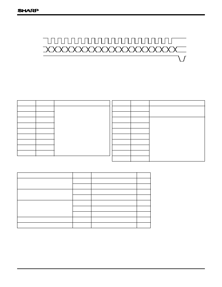
Serial Data Control
SERIAL DATA INPUT TIMING
The serial data ED
1
is shifted by ED
0
and is
latched at the rising edge of ED
2
.
The shutter mode data SMD
1
and SMD
2
of serial
data are latched at the rising edge of the horizontal
line in which VTG is active, the shutter speed data
SD
0
to SD
8
are latched at the rising edge of the
next horizontal line in which VTG is active.
ED
1
ED
2
D
00
D
01
D
02
D
03
D
04
D
05
D
06
D
07
D
08
D
09
D
10
D
11
D
12
D
13
D
14
D
15
D
16
D
17
D
18
ED
0
DATA
D
00
SERIAL DATA INPUTS
D
17
D
16
D
15
D
14
D
13
D
12
D
11
D
10
D
09
D
08
D
07
D
06
D
05
D
04
D
03
D
02
D
01
SD
1
SD
2
SD
3
SD
4
SD
5
SD
6
SD
7
SD
8
SMD
1
SMD
2
MR
1
MR
2
MC
1
MC
2
MS
1
MS
2
MF
1
SD
0
NAME
MF
2
D
18
FUNCTIONS
DATA
NAME
FUNCTIONS
Electronic shutter speed control
Electronic shutter mode control
Phase control
PARAMETER
SYMBOL
RATING
UNIT
Supply voltage
V
DD3
, V
DD5
≠0.3 to +6.0
V
V
DD12
≠0.3 to +15.0
V
Input voltage
V
I3
≠0.3 to V
DD3
+ 0.3
V
Output voltage
V
O3
≠0.3 to V
DD3
+ 0.3
V
Operating temperature
T
OPR
≠20 to +70
∞C
Storage temperature
T
STG
≠55 to +150
∞C
ABSOLUTE MAXIMUM RATINGS
V
≠0.3 to V
DD5
+ 0.3
V
I5
V
≠0.3 to V
DD5
+ 0.3
V
O5
V
O12
≠0.3 to V
DD12
+ 0.3
V
LR38581
7
NOTES :
1. Applied to inputs (IC3, OSCI3).
2. Applied to input (ICU3).
3. Applied to input (ICSU3).
4. Applied to input (ICU5).
5. Applied to input (ICD5).
6. Applied to output (OSCO3). (Output (OSCO3) measures
on condition that input (OSCI3) level is 0 V or V
DD3
.)
7. Applied to output (O4MA3).
8. Applied to output (O4MA32).
9. Applied to output (O4MA52).
10. Applied to output (O4MA53).
11. Applied to output (O12MHV).
ELECTRICAL CHARACTERISTICS
DC Characteristics
(V
DD3
= 3.3±0.33 V, V
DD5
= 5.0±0.5 V, V
DD12
= 12.5±0.5 V, T
OPR
= ≠20 to +70 ∞C)
Input "Low" voltage
V
IL3
Input "High" voltage
V
IH3
Input "Low" voltage
V
IL5
V
IH5
Input "Low" voltage
V
T+
Input "High" voltage
V
T≠
Input "Low" current
|I
IL3-1
|
Input "High" current
|I
IH3-1
|
Input "Low" current
|I
IL3-2
|
Input "High" current
|I
IH3-2
|
Input "Low" current
|I
IL5-1
|
Input "High" current
|I
IH5-1
|
Input "Low" current
|I
IL5-2
|
Input "High" current
|I
IH5-2
|
Output "Low" voltage
V
OL3-1
Output "High" voltage
V
OH3-1
Output "Low" voltage
V
OL3-2
Output "High" voltage
V
OH3-2
Output "Low" voltage
V
OL3-3
Output "High" voltage
V
OH3-3
PARAMETER
SYMBOL
CONDITIONS
Input "High" voltage
V
T+
≠ V
T≠
Hysteresis voltage
MIN.
3.5
0.7V
DD3
V
DD3
≠ 0.5
8.0
8.0
3.0
0.045V
DD3
0.02V
DD3
V
DD3
≠ 0.5
V
DD3
≠ 0.5
TYP.
MAX.
1.5
0.3V
DD3
0.4
0.4
60
2.0
2.0
60
2.0
30
1.0
1.0
0.75V
DD3
I
OL
= 4 mA
I
OH
= ≠1.5 mA
I
OL
= 2 mA
I
OH
= ≠1.5 mA
I
OL
= 1.5 mA
V
I
= V
DD5
V
I
= 0 V
V
I
= V
DD5
V
I
= 0 V
V
I
= V
DD3
V
I
= 0 V
V
I
= V
DD3
V
I
= 0 V
I
OH
= ≠3 mA
0.4
V
V
V
V
µA
µA
µA
µA
µA
µA
µA
µA
V
V
V
V
V
V
V
V
UNIT
V
8
NOTE
4, 5
1, 2
7
6
5
4
2, 3
1
3
11
V
V
I
OL
= 12 mA
I
OH
= ≠12 mA
0.4
V
DD12
≠ 0.5
V
OH12
Output "High" voltage
V
OL12
Output "Low" voltage
10
V
V
I
OL
= 12 mA
I
OH
= ≠9 mA
0.4
V
DD5
≠ 0.5
V
OH5-2
Output "High" voltage
V
OL5-2
Output "Low" voltage
9
V
V
I
OL
= 9 mA
I
OH
= ≠6 mA
0.4
V
DD5
≠ 0.5
V
OH5-1
Output "High" voltage
V
OL5-1
Output "Low" voltage
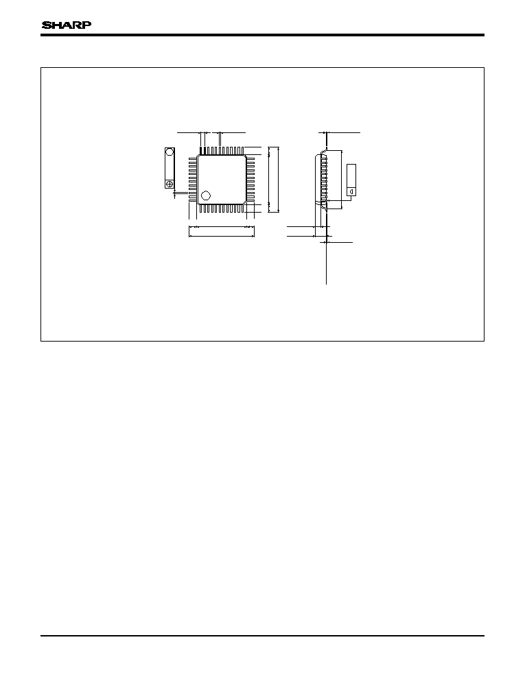
PACKAGES FOR CCD AND CMOS DEVICES
8
36
25
37
48
12
1
0.15
±0.05
0.1
±0.1
9.0
±0.3
7.0
±0.2
7.0
±0.2
(1.0)
(1.0)
(1.0)
(1.0)
0.5
TYP.
0.2
±0.08
9.0
±0.3
0.65
±0.2
1.45
±0.2
24
13
Package
base plane
8.0
±0.2
0.08
0.1
M
48 QFP (QFP048-P-0707)
PACKAGE
(Unit : mm)