 | –≠–Ľ–Ķ–ļ—ā—Ä–ĺ–Ĺ–Ĺ—č–Ļ –ļ–ĺ–ľ–Ņ–ĺ–Ĺ–Ķ–Ĺ—ā: LR38620 | –°–ļ–į—á–į—ā—Ć:  PDF PDF  ZIP ZIP |
DESCRIPTION
The LR38620 is a CMOS timing generator IC
which generates timing pulses for driving 4 200 k-
pixel CCD area sensor and processing pulses.
FEATURES
∑ Designed for 1/1.8-type 4 200 k-pixel CCD area
sensor
∑ Frequency of driving horizontal CCD : 24.54545
MHz
∑ In monitoring mode, it can be obtained 30 fields/s
∑ External shutter control function with serial data
input is possible
∑ +3.3 V and +4.5 V power supplies
∑ Package :
48-pin QFP (P-QFP048-0707) 0.5 mm pin-pitch
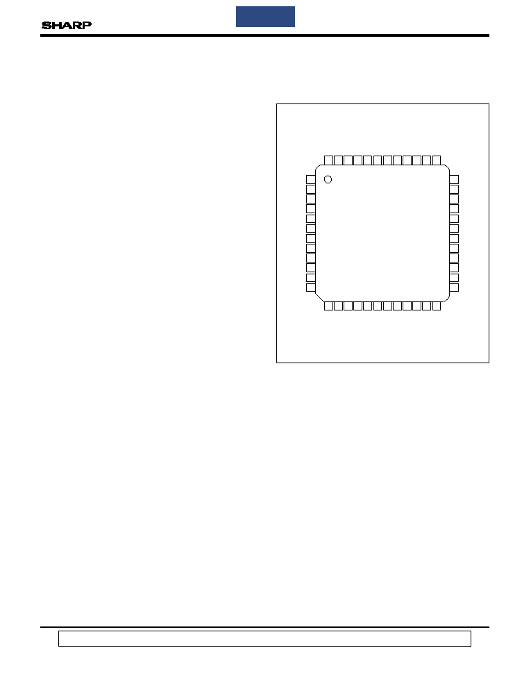
PIN CONNECTIONS
LR38620
1
LR38620
Timing Generator IC for
4 200 k-pixel CCD
1
48 47 46 45 44 43 42 41 40 39
37
13 14 15 16 17 18 19 20 21 22 23 24
2
3
4
5
6
7
8
9
10
11
12
36
35
34
33
32
31
30
29
28
27
26
25
GND
OFDC
OFDX
V
1X
VH
1AX
VH
1BX
V
2X
V
3X
VH
3AX
VH
3BX
V
4X
GND
GND
TST
1
ED
2
ED
1
ED
0
HD
VD
DCLK
CLK
CKO
CKI
GND
V
DD3
V
DD3
PBLK
BCPX
CLPX
ADCK
FCDS
FS
SHTR
ID
V
DD3
V
DD3
V
DD4
V
DD4
TST
3
TST
2
FR
FH
2
GND
GND
FH
1
ACLX
V
DD4
V
DD4
38
48-PIN QFP
TOP VIEW
(P-QFP048-0707)
In the absence of confirmation by device specification sheets, SHARP takes no responsibility for any defects that may occur in equipment using any SHARP devices shown in
catalogs, data books, etc. Contact SHARP in order to obtain the latest device specification sheets before using any SHARP device.
BACK
LR38620
2
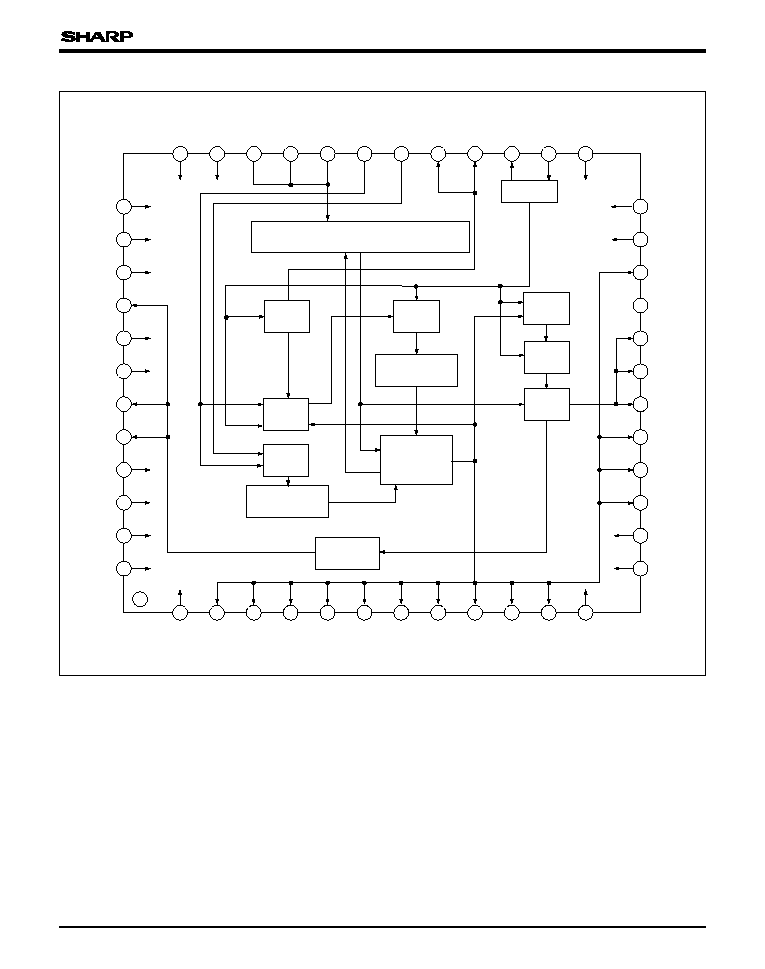
BLOCK DIAGRAM
GND
TST
1
ED
2
ED
1
ED
0
HD
VD
DCLK
CLK
CKO
CKI
GND
36
35
34
33
32
31
30
29
28
27
26
25
V
DD3
V
DD3
ID
SHTR
FS
FCDS
ADCK
CLPX
BCPX
PBLK
V
DD3
V
DD3
GND
OFDC
OFDX
V
1X
VH
1AX
VH
1BX
V
2X
V
3X
VH
3AX
VH
3BX
V
4X
GND
V
DD4
V
DD4
ACLX
FH
1
GND
GND
FH
2
FR
TST
2
TST
3
V
DD4
V
DD4
1/2
1/16
OSC
DATA LATCH & SHUTTER CONTROL
RESET
RESET
RESET
1/2
GATE
H COUNTER
V COUNTER
LEVEL
SHIFTER
DECODER
13
14
15
16
17
18
19
20
21
22
23
24
1
2
3
4
5
6
7
8
9
10
11
12
48
47
46
45
44
43
42
41
40
39
38
37
LR38620
3
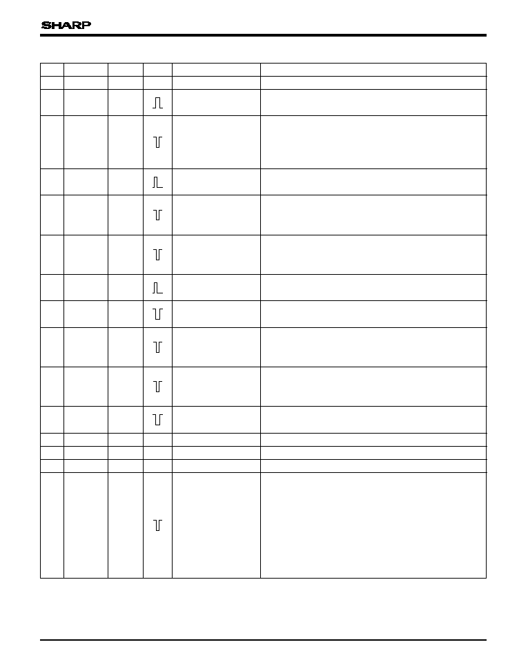
PIN NO. SYMBOL IO SYMBOL POLARITY
PIN NAME
DESCRIPTION
1
GND
≠
GroundA ground
ing pin.
2
OFDC
O3MR1
Control pulse output
for OFD voltage
A pulse to control OFD voltage.
3
OFDX
O3MR1
OFD pulse output
A pulse that sweeps the charge of the photo-diode for
the electronic shutter. Connect to OFD pin of the CCD
through the vertical driver IC and DC offset circuit.
Held at H level in normal mode.
4
V
1X
O3MR1
Vertical transfer
pulse output 1
A vertical transfer pulse for the CCD.
Connect to V
1X
pin of vertical driver IC.
5
VH
1AX
O3MR1
Readout pulse
output 1A
A pulse that transfers the charge of the photo-diode to
the vertical shift register.
Connect to VH
1AX
pin of vertical driver IC.
PIN DESCRIPTION
≠
A pulse that transfers the charge of the photo-diode to
the vertical shift register.
Connect to VH
1BX
pin of vertical driver IC.
Readout pulse
output 1B
O3MR1
VH
1BX
6
7
V
2X
O3MR1
Vertical transfer
pulse output 2
A vertical transfer pulse for the CCD.
Connect to V
2X
pin of vertical driver IC.
A vertical transfer pulse for the CCD.
Connect to V
3X
pin of vertical driver IC.
Vertical transfer
pulse output 3
O3MR1
V
3X
8
9
VH
3AX
O3MR1
Readout pulse
output 3A
A pulse that transfers the charge of the photo-diode to
the vertical shift register.
Connect to VH
3AX
pin of vertical driver IC.
A pulse that transfers the charge of the photo-diode to
the vertical shift register.
Connect to VH
3BX
pin of vertical driver IC.
Readout pulse
output 3B
O3MR1
VH
3BX
10
11
V
4X
O3MR1
Vertical transfer
pulse output 4
A vertical transfer pulse for the CCD.
Connect to V
4X
pin of vertical driver IC.
A grounding pin.
Ground
≠
GND
12
≠
≠
13
V
DD3
≠
Power supply
Supply of +3.3 V power.
Supply of +3.3 V power.
Power supply
≠
V
DD3
14
≠
15
PBLK
O3MR1
Pre-blanking pulse
output
A pulse for pre-blanking. This pulse is controlled by
serial data BLKCNT.
BLKCNT = H; This pulse stays low during the
absence of effective pixels within the
vertical blanking or during the
sweepout signal.
BLKCNT = L; Continuous pulse
The output phase of PBLK is selected by serial data.
LR38620
4
PIN NO. SYMBOL IO SYMBOL POLARITY
PIN NAME
DESCRIPTION
16
BCPX
O3MR1
Optical black clamp
pulse output
A pulse to clamp the optical black signal.
This pulse is controlled by serial data BCPCNT.
BCPCNT = H; This pulse stays high during the
absence of effective pixels within the
vertical blanking or during the
sweepout signal.
BCPCNT = L; This pulse stays high during the
sweepout signal.
A pulse to clamp the dummy outputs of the CCD signal.
This pulse stays high during the sweepout period.
Clamp pulse output
O3MR1
CLPX
17
18
ADCK
O6M32
AD clock output
An output pin for AD converter. The output phase of
ADCK is selected by serial data in 90į steps.
A pulse to clamp the feed-through level for the CCD.
The output phase and output polarity of FCDS are
selected by serial data.
CDS pulse output 1
O6M32
FCDS
19
20
FS
O6M32
CDS pulse output 2
A pulse to sample-hold the signal for the CCD.
The output phase and output polarity of FS are selected
by serial data.
A trigger pulse for effective signal period.
Trigger output
O3MR1
SHTR
21
22
ID
O3MR1
Line index pulse
output
The pulse is used in the color separator.
The signal switches between high and low at every line.
Supply of +3.3 V power.
Power supply
≠
V
DD3
23
≠
≠
24
V
DD3
≠
Power supply
Supply of +3.3 V power.
A grounding pin.
Ground
≠
GND
25
≠
≠
26
CKI
OSCI3
Clock input
An input pin for reference clock oscillation.
The frequency is 49.0909 MHz.
An output pin for reference oscillation.
The output is the inverse of CKI (pin 26).
Clock output
OSCO3
CKO
27
≠
An output pin to generate HD and VD pulses.
The frequency is 24.54545 MHz.
Clock output
O6M32
CLK
28
29
DCLK
O6M32
Clock output
An output pin for DSP IC. The frequency is 24.54545 MHz.
The output phase of DCLK is selected by serial data in
90į steps.
An input pin for reference of vertical pulse.
Connect to VD pin of DSP IC.
Vertical reference
pulse input
IC3
VD
30
31
HD
IC3
Horizontal drive
pulse input
An input pin for reference of horizontal pulse.
Connect to HD pin of DSP IC.
An input pin for the strobe pulse, to control the functions
of LR38620. For details, see "Serial Data Control".
Strobe pulse input
ICSD3
ED
0
32
≠
≠
33
ED
1
ICSD3
Shift register clock
input
An input pin for the clock of the shift register, to control
the functions of LR38620. For details, see "Serial Data
Control".

LR38620
5
PIN NO. SYMBOL IO SYMBOL POLARITY
PIN NAME
DESCRIPTION
IC3
: Input pin (CMOS level)
ICD3
: Input pin (CMOS level with pull-down resistor)
ICSD3
: Input pin (CMOS schmitt-trigger level with pull-
down resistor)
ICD4
: Input pin (CMOS level with pull-down resistor)
ICU4
: Input pin (CMOS level with pull-up resistor)
O3MR1
: Output pin (output high level is V
DD3
.)
O6M32
: Output pin (output high level is V
DD3
.)
O8M43
: Output pin (output high level is V
DD4
.)
OSCI3
: Input pin for oscillation
OSCO3
: Output pin for oscillation
An input pin for the data of the shift register, to control
the functions of LR38620. For details, see "Serial Data
Control".
Shift register data
input
ICSD3
ED
2
34
≠
≠
35
TST
1
ICD3
Test pin 1
A test pin. Set open or to L level in normal mode.
A grounding pin.
Ground
≠
GND
36
≠
≠
37
V
DD4
≠
Power supply
Supply of +4.5 V power.
Supply of +4.5 V power.
Power supply
≠
V
DD4
38
≠
≠
39
ACLX
ICU4
All clear input
An input pin for resetting all internal circuit at power-on.
Connect to V
DD3
through the diode and GND through
the capacitor.
A horizontal transfer pulse for the CCD.
Connect to ō
H1
pin of the CCD.
Horizontal transfer
pulse output 1
O8M43
FH
1
40
42
GND
≠
GroundA ground
ing pin.
41
GND
≠
GroundA ground
ing pin.
≠
≠
A horizontal transfer pulse for the CCD.
Connect to ō
H2
pin of the CCD.
Horizontal transfer
pulse output 2
O8M43
FH
2
43
44
FR
O8M43
Reset pulse output
A pulse to reset the charge of output circuit.
The output phase of FR is selected by serial data.
A test pin. Set open or to L level in normal mode.
Test pin 2
ICD4
TST
2
45
≠
≠
46
TST
3
ICD4
Test pin 3
A test pin. Set open or to L level in normal mode.
Supply of +4.5 V power.
Power supply
≠
V
DD4
48
≠
Supply of +4.5 V power.
Power supply
≠
V
DD4
47
≠
LR38620
6
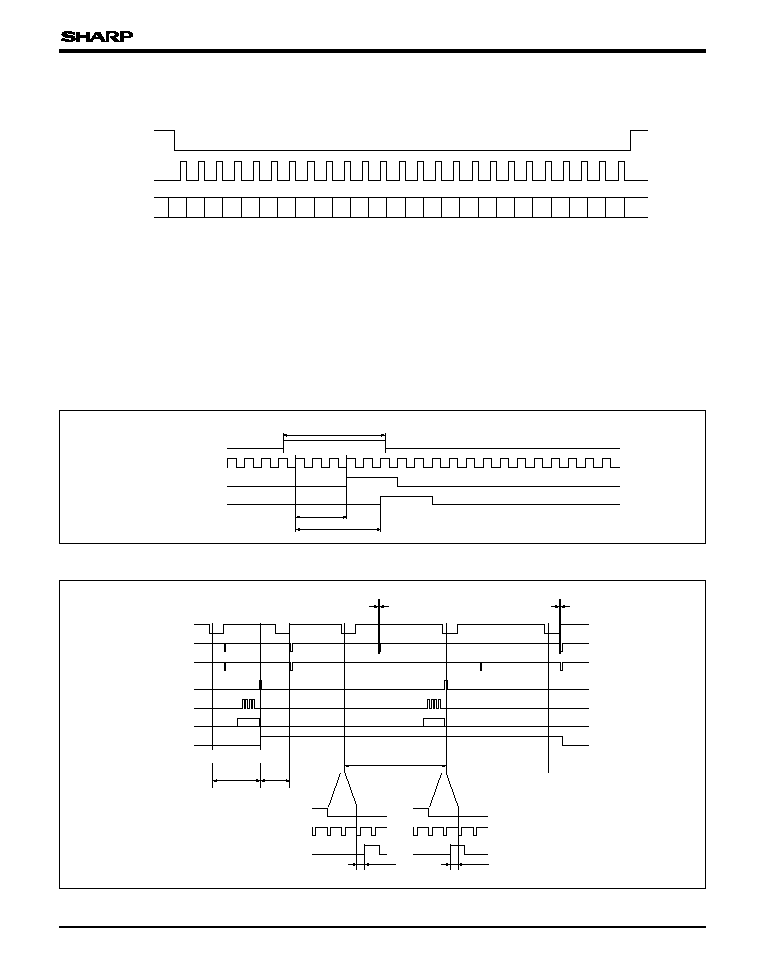
Serial Data Control
SERIAL DATA INPUT TIMING
ED
2
is shifted by the rising edge of ED
1
, and is
latched by the pulse #1 which is generated after
122 to 162 ns delay from the rising edge of ED
0
.
(See Fig. 2.)
The latched serial data are divided into two types
by the data of D
00
, and are relatched by the pulse
#2 which is generated after 203 to 243 ns delay
from the rising edge of ED
0
. (See Fig. 1.)
INMD is effective at the start of #3 horizontal line,
and shutter control data are effective at the start of
#11 horizontal line in monitoring mode and #93
horizontal line in still mode, and other data are
effective at pulse #2.
ED
0
should be at low level during data inputs of
ED
1
and ED
2
or while ACLX is at low level.
ED
0
ED
1
ED
2
D
22
D
21
D
23
D
24
D
20
D
19
D
18
D
17
D
16
D
15
D
14
D
09
D
10
D
08
D
07
D
06
D
05
D
04
D
03
D
02
D
01
D
00
D
11
D
12
D
13
Pulse #2
Pulse #1
ED
0
24.54545 MHz
244 ns min.
122 ns
203 ns
Fig. 1 Data Latch Timing
ED
0
ED
1
ED
2
OFDC
VH
3AX
VD
Monitoring
data input
period
10 ms min.
Mode
Monitoring
Still
Odd Field
Even Field
VH
1AX
from still mode to monitoring mode
data input period
5 Ķs min.
VD
HD
ED
0
5 Ķs min.
from monitoring mode
to still mode
Fig. 2 Input Pulse Timing of ED
0
, ED
1
and ED
2
LR38620
7
SERIAL DATA INPUTS
DATA
D
00
= L
NAME
FUNCTION
DATA = L
DATA = H
AT ACLX = L
D
01
-D
09
SDV
0
-SDV
8
Integration time control in field
period step by horizontal period.
≠
All L
All L
Fix to L level
Dummy
SDH
0
-SDH
5
D
10
-D
15
D
16
SDF
0
Integration time control by field
period.
≠
All L
SDF
1
SDF
2
D
17
D
18
D
24
D
23
VHCNT
Dummy
L
Fix to L level
Dummy
Dummy
D
22
D
21
D
20
INMD
PWSA
L
≠
Electronic shutter mode control
SMD
D
19
Power save control
Integration mode control
Normal
Monitoring
L
L
Dummy
VH
1AX
to VH
3BX
control
Fix to L level
Output
L
L
Held at H level
Still
Power save
D
00
= H
DATA
NAME
FUNCTION
DATA = L
DATA = H
AT ACLX = L
D
01
ML1
Phase control
≠
All L
ML2
D
02
D
04
MR2
All L
≠
MR1
D
03
MR3
D
05
D
08
MC3
D
06
MC1
≠
All L
MC2
D
07
D
10
MS2
All L
≠
MS1
D
09
MS3
D
11
D
14
MD3
D
12
MD1
≠
All L
MD2
D
13
D
16
MA2
All L
≠
MA1
D
15
D
17
Dummy
Fix to L level
All L
Dummy
D
18
D
19
Dummy
D
21
MP2
All L
≠
MP1
D
20
D
22
PLCH
Polarity control of FCDS and FS
pulses
Negative
Positive
L
BLKCNT
D
23
L
Continuous
PBLK control
Discontinuous
BCPX control
Continuous
L
D
24
BCPCNT
Phase control
Dummy
Discontinuous
LR38620
8
ELECTRICAL CHARACTERISTICS
DC Characteristics
(V
DD3
= 3.3Ī10%, V
DD4
= 4.5Ī10%, T
OPR
= ≠20 to +70įC)
NOTES :
1. Applied to inputs (IC3, OSCI3).
2. Applied to input (ICD3).
3. Applied to input (ICSD3).
4. Applied to input (ICU4).
5. Applied to input (ICD4).
6. Applied to outputs (OSCO3, O3MR1). (Output (OSCO3)
measures on condition that input (OSCI3) level is 0 V or
V
DD3
.)
7. Applied to output (O6M32).
8. Applied to output (O8M43).
ABSOLUTE MAXIMUM RATINGS
PARAMETER
SYMBOL
Supply voltage
V
DD3,
V
DD4
V
I3
V
O3
T
OPR
T
STG
≠55 to +150
≠20 to +70
≠0.3 to V
DD3
+ 0.3
≠0.3 to V
DD3
+ 0.3
≠0.3 to +5.5
RATING
UNIT
V
V
V
įC
įC
Storage temperature
Operating temperature
Output voltage
Input voltage
V
I4
V
O4
≠0.3 to V
DD4
+ 0.3
≠0.3 to V
DD4
+ 0.3
V
V
Input "Low" voltage
V
IL3-1
Input "High" voltage
V
IH3-1
Input "Low" voltage
V
IL3-2
V
IH3-2
Hysteresis voltage
V
T+
≠ V
T≠
Input "Low" voltage
V
IL4
Input "Low" current
|I
IL3-1
|
Input "High" current
|I
IH3-1
|
Input "Low" current
|I
IL3-2
|
Input "Low" current
|I
IL4-1
|
Input "High" current
|I
IH4-1
|
Input "Low" current
|I
IL4-2
|
Input "High" current
|I
IH4-2
|
Output "Low" voltage
V
OL3-1
Output "High" voltage
V
OH3-1
Output "Low" voltage
V
OL3-2
Output "High" voltage
V
OH3-2
Output "Low" voltage
Output "High" voltage
V
OH4
PARAMETER
SYMBOL
CONDITIONS
Input "High" voltage
V
IH4
Input "High" voltage
MIN.
0.2V
DD3
0.8V
DD3
V
DD3
≠ 0.5
20
20
0.8V
DD4
0.14V
DD3
V
DD4
≠ 0.5
V
DD3
≠ 0.5
TYP.
0.4
MAX.
0.75V
DD3
0.2V
DD3
0.4
300
5.0
5.0
300
3.0
1.0
1.0
0.2V
DD4
0.4
Schmitt-buffer
I
OH
= ≠10 mA
I
OL
= 12 mA
I
OH
= ≠2.5 mA
I
OL
= 3 mA
V
I
= V
DD4
V
I
= 0 V
V
I
= V
DD4
V
I
= 0 V
V
I
= 0 V
V
I
= V
DD3
V
I
= 0 V
I
OH
= ≠20 mA
V
Output "Low" voltage
V
OL4
0.4
I
OL
= 20 mA
V
V
V
V
V
ĶA
ĶA
ĶA
ĶA
ĶA
ĶA
ĶA
V
V
V
V
V
V
V
UNIT
V
7
NOTE
3
1, 2
6
5
4
8
1
ĶA
V
I
= V
DD3
100
8.0
|I
IH3-2
|
Input "High" current
2, 3
4, 5
LR38620
9
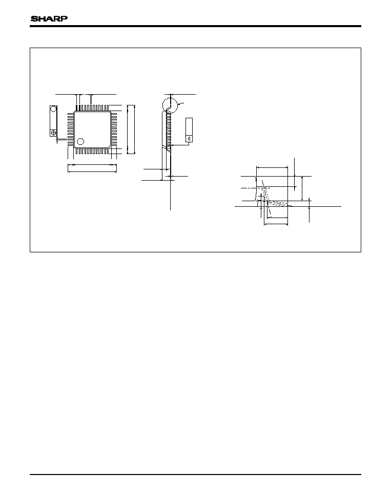
36
25
37
48
12
1
0.15
Ī0.05
See Detail A
0.1
Ī0.1
9.0
Ī0.3
7.0
Ī0.2
7.0
Ī0.2
(1.0)
(1.0)
(1.0)
(1.0)
P-0.5
TYP.
48-0.2
Ī0.08
9.0
Ī0.3
0.65
Ī0.2
1.45
Ī0.2
24
13
0.08
0.10
M
0-10į
0.65
Ī0.2
0.6
Ī0.15
0.5
1.0
Ī0.15
1.45
Ī0.2
Seating plane
Package
base plane
Detail A
0.1
Ī0.1
0.25
48 QFP (P-QFP048-0707)
(Unit : mm)
PACKAGE OUTLINES