 | –≠–ª–µ–∫—Ç—Ä–æ–Ω–Ω—ã–π –∫–æ–º–ø–æ–Ω–µ–Ω—Ç: LRS1331 | –°–∫–∞—á–∞—Ç—å:  PDF PDF  ZIP ZIP |
Data Sheet
1
LRS1331
Data Sheet
Stacked Chip
16M Flash Memory and 4M SRAM
FEATURES
∑ Flash Memory and SRAM
∑ Stacked Die Chip Scale Package
∑ 72-ball 8 mm ◊ 11 mm CSP plastic package
∑ Power supply: 2.7 V to 3.6 V
∑ Operating temperature: -25∞C to +85∞C
∑ Flash Memory
≠ Access time (MAX.): 90 ns
≠ Operating current (MAX.)
(The current for F-V
CC
pin and F-V
CCW
pin):
≠ Read: 25 mA (t
CYCLE
= 200 ns)
≠ Word write: 57 mA
≠ Block erase: 42 mA
≠ Standby current (the current for F-V
CC
pin): 15 µA
(MAX. F-RP
GND ± 0.2 V)
≠ Optimized array blocking architecture
≠ Two 4K-word boot blocks
≠ Six 4K-word parameter blocks
≠ Thirty-one 32K-word main blocks
≠ Bottom boot location
≠ Extended cycling capability
≠ 100,000 block erase cycles
≠ Enhanced automated suspend options
≠ Word write suspend to read
≠ Block erase suspend to word write
≠ Block erase suspend to read
∑ SRAM
≠ Access time (MAX.): 85 ns
≠ Operating current: 45 mA (MAX.)
≠ Standby current: 15 µA (MAX.)
≠ Data retention current: 2 µA (MAX.)
DESCRIPTION
The LRS1331 is a combination memory organized as
1,048,576 ◊ 16-bit flash memory and 262,144 ◊ 16-bit
static RAM in one package.
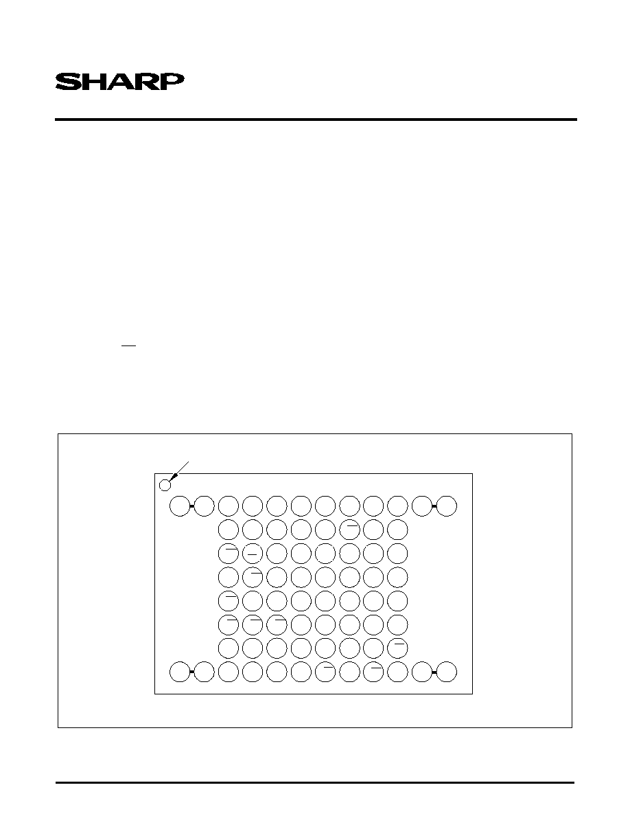
PIN CONFIGURATION
Figure 1. LRS1331 Pin Configuration
A
INDEX
A
11
A
15
NC
NC
NC
A
14
A
9
1
2
3
4
5
6
7
A
16
DQ
15
DQ
14
S-V
CC
A
8
A
10
T
1
S-A
17
DQ
13
DQ
12
GND
T
4
F-WE
F-RY/
BY
F-RP
T
2
F-WP
F-V
PP
F-A
19
DQ
11
T
3
B
C
D
E
F
S-LB S-UB S-OE
NC
DQ
9
8
DQ
6
DQ
10
DQ
8
F-A
18
F-A
17
A
7
A
6
A
3
A
2
NC
NC
G
H
NC
A
5
A
4
A
0
F-OE
F-CE
F-GND
NC
NC
F-GND
A
12
A
13
9
10
S-WE
DQ
4
S-CE
2
DQ
2
DQ
0
11
A
1
NC
NC
NC
12
DQ
7
DQ
5
F-V
CC
DQ
3
DQ
1
S-CE
1
NC
LRS1331-1
TOP VIEW
72-BALL FBGA
NOTE: All F-GND and S-GND pins are connected on the board.
Two NC pins at the corner are connected.
LRS1331
Stacked Chip (16M Flash & 4M SRAM)
2
Data Sheet
Figure 2. LRS1331 Block Diagram
LRS1331-2
16M (x16) BIT
FLASH MEMORY
4M (x16) BIT
SRAM
F-A
17
to
F-A
19
F-RY/BY
F-V
CC
F-V
PP
S-GND
S-V
CC
F-GND
DQ
0
to
DQ
15
F-CE
F-OE
F-WE
F-RP
F-WP
A
0
to A
16
S-CE
1
S-CE
2
S-OE
S-WE
S-A
17
S-UB
S-LB
Stacked Chip (16M Flash & 4M SRAM)
LRS1331
Data Sheet
3
Table 1. Pin Descriptions
PIN
DESCRIPTION
TYPE
A
0
to A
16
Address Inputs (Common)
Input
F-A
17
to F-A
19
Address Inputs (Flash)
Input
S-A
17
Address Input (SRAM)
Input
F-CE
Chip Enable Input (Flash)
Input
S-CE
1
, S-CE
2
Chip Enable Inputs (SRAM)
Input
F-WE
Write Enable Input (Flash)
Input
S-WE
Write Enable Input (SRAM)
Input
F-OE
Output Enable Input (Flash)
Input
S-OE
Output Enable Input (SRAM)
Input
S-LB
SRAM Byte Enable Input (DQ
0
to DQ
7
)
Input
S-UB
SRAM Byte Enable Input (DQ
8
to DQ
15
)
Input
F-RP
Deep Power Down Input (Flash)
Block erase and Word Write: V
IH
Read: V
IH
Deep Power Down: V
IL
Input
F-WP
Write Protect Input (Flash)
Two Boot Blocks Locked: V
IL
Input
F-RY/BY
Ready/Busy Output(Flash)
During an Erase or Write operation: V
OL
Block Erase and Word Write Suspend: HIGH-Z
Deep Power Down: V
OH
Output
DQ
0
to DQ
15
Data Input and Outputs (Common)
Input/Output
F-V
CC
Power Supply (Flash)
Power
S-V
CC
Power Supply (SRAM)
Power
F-V
PP
Write, Erase Power Supply (Flash)
Block Erase and Word Write: F-V
PP
= V
PPLK
All Blocks Locked: F-V
PP
< V
PPLK
Power
F-GND
Ground (Flash)
Power
S-GND
Ground (SRAM)
Power
NC
No Connection
--
T
1
to T
5
Test Pins (Should be Open)
--
LRS1331
Stacked Chip (16M Flash & 4M SRAM)
4
Data Sheet
NOTES:
1. L = V
IL
, H = V
IH
, X = H or L. Refer to DC Characteristics.
2. Refer to the `Flash Memory Command Definition' section for valid
address input and D
IN
during a write operation.
3. F-WP set to V
IL
or V
IH
.
4. SRAM standby data. See Table 2a.
5. Command writes involving block erase or word write are reliably
executed when V
CCWH
(2.7 V to 3.6 V) and F-V
CC
= 2.7 V to
3.6 V. Block erase or word write with F-V
CCW
< V
CCWH
(MIN.)
produce spurious results and should not be attempted.
6. Never hold F-OE LOW and F-WE LOW at the same timing.
7. S-LB, S-UB Control Mode. See Table 2b.
Table 2. Truth Table
1
FLASH
SRAM
F-CE
F-RP
F-OE
F-WE
S-CE
1
S-CE
2
S-OE
S-WE
S-LB
S-UB
DQ
0
-
DQ
7
DQ
8
-
DQ
15
NOTES
Read
Standby
L
H
L
H
See Note 4
X
X
See Note 4
D
OUT
2, 3
Output Disable
Standby
L
H
H
H
X
X
HIGH-Z
3
Write
Standby
L
H
H
L
X
X
D
IN
2, 3, 5, 6
Standby
Read
H
H
X
X
L
H
L
H
See Note 7
Output
Disable
H
H
X
X
L
H
H
H
X
X
HIGH-Z
H
H
X
X
L
H
X
X
H
H
HIGH-Z
Write
H
H
X
X
L
H
L
L
See Note 7
Reset
Read
X
L
X
X
L
H
L
H
Output
Disable
X
L
X
X
L
H
H
H
X
X
HIGH-Z
X
L
X
X
L
H
X
X
H
H
HIGH-Z
Write
X
L
X
X
L
H
L
L
See Note 7
Standby
Standby
H
H
X
X
See Note 4
X
X
See Note 4
HIGH-Z
3
Reset
Standby
X
L
X
X
X
X
HIGH-Z
3
Table 2a.
MODE
PINS
S-CE
1
S-CE
2
S-LB
S-UB
Standby
(SRAM)
H
X
X
X
X
L
X
X
X
X
H
H
Table 2b.
MODE
(SRAM)
PINS
S-LB
S-UB
DQ
0
- DQ
7
DQ
8
- DQ
15
Read/Write
L
L
D
OUT
/D
IN
D
OUT
/D
IN
L
H
D
OUT
/D
IN
HIGH-Z
H
L
HIGH-Z
D
OUT
/D
IN
Stacked Chip (16M Flash & 4M SRAM)
LRS1331
Data Sheet
5
NOTES:
1. Commands other than those shown in table are reserved by SHARP for future device
implementations and should not be used.
2. BUS operations are defined in Table 2.
3. XA = Any valid address within the device;
IA = Identifier code address;
BA = Address within the block being erased;
WA = Address of memory location to be written;
SRD = Data read from status register;
WD = Data to be written at location WA. Data is latched on the
rising edge of F-WE or F-CE (whichever goes HIGH first);
ID = Data read from identifier codes.
4. See Table 4 for Identifier Codes.
5. See Table 5 for Write Protection Alternatives.
6. If the permanent lock-bit is set, Set Block Lock-Bit and Clear Block Lock-Bits commands cannot be done.
7. The clear block lock-bits operation simultaneously clears all block lock-bits.
NOTES:
1. DQ
8
- DQ
15
outputs 00H in word mode. DQ
1
- DQ
7
are reserved for future use.
2. BA selects the specific block lock configuration code to be read. See Figure 3
for the device identifier code memory map.
Table 3. Command Definition for Flash Memory
1
COMMAND
BUS CYCLES
REQUIRED
FIRST BUS CYCLE
SECOND BUS CYCLE
NOTES
OPERATION
2
ADDRESS
3
DATA
3
OPERATION
2
ADDRESS
3
DATA
3
Read Array/Reset
1
Write
XA
FFH
Read Identifier Codes
2
Write
XA
90H
Read
IA
ID
4
Read Status Register
2
Write
XA
70H
Read
XA
SRD
Clear Status Register
1
Write
XA
50H
Block Erase
2
Write
BA
20H
Write
BA
D0H
5
Full Chip Erase
2
Write
XA
30H
Write
XA
D0H
Word Write
2
Write
WA
40H or 10H
Write
WA
WD
5
Block Erase and Word
Write Suspend
1
Write
XA
B0H
5
Block Erase and
Write Resume
1
Write
XA
D0H
5
Set Block Lock-Bits
2
Write
BA
60H
Write
BA
01H
6
Clear Block Lock-Bits
2
Write
XA
60H
Write
XA
D0H
6, 7
Set Permanent Lock-Bits
2
Write
XA
60H
Write
XA
F1H
Table 4. Identifier Codes
CODES
ADDRESS (A
0
- A
19
)
DATA (DQ
0
- DQ
7
)
1
NOTES
Manufacture Code
00000H
B0H
Device Code
00001H
E9H
Block Lock
Configuration
Block is Unlocked
BA + 2
DQ
0
= 0
2
Block is Locked
BA + 2
DQ
0
= 1
2
Permanent Lock
Configuration
Device is Unlocked
00003H
DQ
0
= 0
Device is Locked
00003H
DQ
0
= 1