Data Sheet
1
LRS1338A
Data Sheet
Stacked Chip
8M Flash Memory and 2M SRAM
FEATURES
∑ Flash memory and SRAM
∑ Stacked die chip scale package
∑ 48-pin TSOP (TSOP48-P-1014) plastic package
∑ Power supply: 2.7 V to 3.6 V
∑ Operating temperature: -40∞C to +85∞C
∑ Access time (MAX.):
≠ Flash memory: 120 ns
≠ SRAM: 85 ns
∑ Operating current (MAX.):
≠ Flash memory
≠ Read: 25 mA (t
CYCLE
= 200 ns)
≠ Word write: 57 mA (F-V
CC
3.0 V)
≠ Block erase: 42 mA (F-V
CC
3.0 V)
≠ SRAM: 25 mA (t
CYCLE
= 200 ns)
∑ Standby current
2
≠ Flash memory: 20 µA MAX. (F-CE
F-V
CC
- 0.2 V,
F-RP
0.2 V, F-V
PP
0.2 V)
≠ SRAM:
≠ 40 µA MAX. (S-CE
S-V
CC
- 0.2 V)
≠ 0.6 µA TYP. (T
A
= 25∞C, S-V
CC
= 3 V,
S-CE
S-V
CC
- 0.2 V)
∑ Fully static operation
∑ Three-state output
NOTES:
1. Block erase and word write operations of flash memory with
T
A
< -30∞C are not supported.
2. Total standby current is the summation of flash's memory standby
current and SRAM's one.
DESCRIPTION
The LRS1338A is a combination memory organized
as 524,288 ◊ 16-bit flash memory and 262,144 ◊ 8-bit
static RAM in one package. It is fabricated using silicon-
gate CMOS process technology.
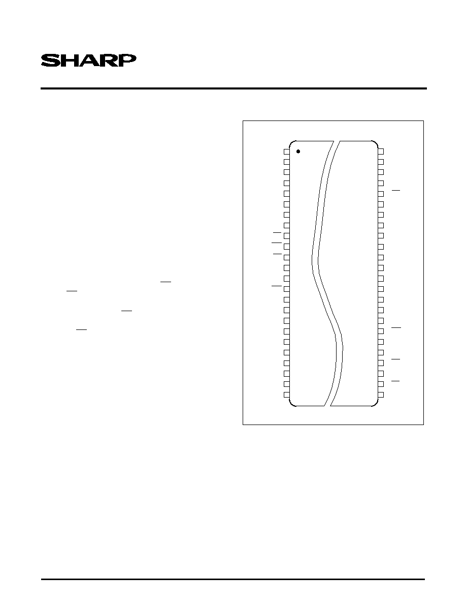
PIN CONFIGURATION
Figure 1. LRS1338A Pin Configuration
LRS1338A-1
TOP VIEW
48-PIN TSOP
2
3
4
5
8
9
S-A
9
/F-A
8
S-A
12
/F-A
11
S-A
13
/F-A
12
S-A
14
/F-A
13
48
45
42
6
7
S-A
10
/F-A
9
S-A
11
/F-A
10
47
46
I/O
14
S-CE
I/O
15
I/O
13
10
11
12
I/O
7
13
44
I/O
3
43
I/O
10
I/O
6
14
15
16
17
18
19
20
39
36
41
40
38
37
I/O
1
S-WE
I/O
8
S-A
7
/F-A
6
S-A
6
/F-A
5
S-A
8
/F-A
7
F-A18
F-A17
F-WP
S-A
5
/F-A
4
I/O
0
F-OE
I/O
5
I/O
4
I/O
12
I/O
9
1
S-A
15
/F-A
14
S-A
16
/F-A
15
S-A
17
/F-A
16
21
22
23
24
S-A
0
S-A
2
/F-A
1
S-A
4
/F-A
3
S-A
3
/F-A
2
34
F-CE
35
GND
31
33
32
30
29
S-A
1
/F-A
0
F-RP
F-WE
S-OE
F-V
PP
S-V
CC
F-V
CC
I/O
11
I/O
2
27
28
26
25
LRS1338A
Stacked Chip (8M Flash & 2M SRAM)
2
Data Sheet
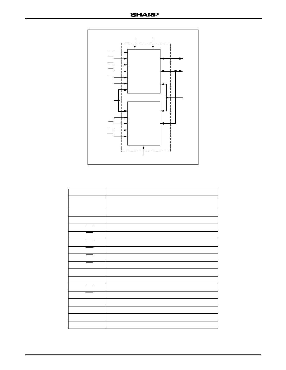
Figure 2. LRS1338A Block Diagram
Table 1. Pin Descriptions
PIN
DESCRIPTION
S-A
1
to S-A
17
F-A
0
to F-A
16
Common Address Input Pins
S-A
0
Address Input Pin for SRAM
F-A
17
to F-A
18
Address Input Pin for Flash Memory
F-CE
Chip Enable Input Pin for Flash Memory
S-CE
Chip Enable Input Pin for SRAM
F-WE
Write Enable Input Pin for Flash Memory
S-WE
Write Enable Input Pin for SRAM
F-OE
Output Enable Input Pin for Flash Memory
S-OE
Output Enable Input Pin for SRAM
I/O
0
to I/0
7
Common Data Input/Output Pins
I/O
8
to I/O
15
Data Input/Output Pins for Flash Memory
F-RP
Reset/Deep Power Down Input Pin for Flash Memory
F-WP
Write Protect Pin for Flash Memory's Boot Block
F-V
CC
Power Supply Pin for Flash Memory
F-V
PP
Power Supply Pin for Flash Memory Write/Erase
S-V
CC
Power Supply Pin for SRAM
GND
Common Ground
LRS1338A-2
524,288 x 16 BIT
FLASH MEMORY
262,144 x 8 BIT
SRAM
F-CE
GND
F-V
CC
S-V
CC
F-V
PP
I/O
0
to
I/O
7
I/O
8
to
I/O
15
F-WE
F-RP
F-WP
F-A
17
, F-A
18
S-A
1
to S-A
17
,
F-A
0
to F-A
16
F-OE
S-A
0
S-CE
S-OE
S-WE

Stacked Chip (8M Flash & 2M SRAM)
LRS1338A
Data Sheet
3
GENERAL DESIGN GUIDELINES
Supply Power
Maximum difference (between F-V
CC
and S-V
CC
) of
the voltage is less than 0.3 V.
Power Supply and Chip Enable of Flash
Memory and SRAM
It is forbidden that both F-CE and S-CE should be
LOW simultaneously. If the two memories are active
together, they many not operate normally due to inter-
ference noises or data collision on I/O bus. Both F-V
CC
and S-V
CC
need to be applied by the recommended
supply voltage at the same time except SRAM data
retention mode.
SRAM Data Retention
SRAM data retention is capable in three ways.
SRAM power switching between a system battery and
a backup battery needs careful device decoupling from
Flash Memory to prevent SRAM supply voltage from
falling lower than 2.0 V by a Flash Memory peak cur-
rent caused by transition of Flash Memory supply volt-
age or of control signals (F-CE, F-OE, and RP).
CASE 1: FLASH MEMORY IS IN STANDBY MODE
(F-V
CC
= 2.7 V TO 3.6 V)
∑ SRAM inputs and input/outputs except S-CE need to
be applied with voltages in the range of -0.3 V to
S-V
CC
+ 0.3 V or to be open (HIGH-Z).
∑ Flash Memory inputs and input/outputs except F-CE
and RP need to be applied with voltages in the range
of -0.3 V to S-V
CC
+ 0.3 V or to be open (HIGH-Z).
CASE 2: FLASH MEMORY IS IN DEEP POWER
DOWN MODE (F-V
CC
= 2.7 V TO 3.6 V)
∑ SRAM inputs and input/outputs except S-CE need to
be applied with voltages in the range of -0.3 V to
S-V
CC
+ 0.3 V or to be open.
∑ Flash Memory inputs and input/outputs except RP
need to be applied with voltages in the range of -0.3 V
to S-V
CC
+ 0.3 V or to be open (HIGH-Z). RP needs to
be at the same level as F-V
CC
or to be open.
CASE 3: FLASH MEMORY POWER SUPPLY IS
TURNED OFF (F-V
CC
= 0 V)
∑ Fix RP LOW level before turning off Flash memory
power supply.
∑ SRAM inputs and input/outputs except S-CE need to
be applied with voltages in the range of -0.3 V to
S-V
CC
+ 0.3 V or to be open (HIGH-Z).
∑ Flash Memory inputs and input/outputs except RP
need to be applied with voltages in the range of
-0.3 V to S-V
CC
+ 0.3 V or to be open (HIGH-Z).
Power Up Sequence
When turning on Flash memory power supply, keep
RP LOW. After F-V
CC
reaches over 2.7 V, keep RP
LOW for more than 100 ns.
Device Decoupling
The power supply needs to be designed carefully
because one of the SRAM and the Flash Memory is in
standby mode when the other is active. A careful
decoupling of power supplies is necessary between
SRAM and Flash Memory. Note peak current caused
by transition of control signals (F-CE, S-CE).
NOTES:
1. F-CE should not be LOW when S-CE is LOW simultaneously.
2. X can be V
IL
or V
IH
for control pins and addresses, and V
PPLK
or V
PPH
for F-V
PP
. See DC Characteristics for V
PPLK
and V
PPH
voltages.
3. Refer to DC Characteristics. When F-V
PP
V
PPLK
, memory con-
tents can be read, but not altered.
4. Do not use in a timing that both F-OE and F-WE is LOW level.
5. F-RP at GND ± 0.2 V ensures the lowest deep power down current.
6. Command writes involving block erase, write, or lock-bit configura-
tion are reliably executed when F-V
PP
= V
PPH
and F-V
CC
= V
CC1
block erase or word write operations with V
IH
< F-RP < V
HH
or
T
A
< -30∞C produce spurious results and should not be attempted.
7. Refer to Table 6 for valid D
IN
during a write operation.
Table 2. Truth Table
1,2
F-CE
F-OE
F-WE
F-RP
S-CE
S-OE
S-WE
ADDRESS
MODE
I/O
0
to
I/O
15
CURRENT
NOTE
L
L
H
H
H
X
X
X
Flash read
Output
I
CC
3, 4
L
H
H
H
H
X
X
X
Flash read
HIGH-Z
I
CC
5
L
H
L
H
H
X
X
X
Flash write
Input
I
CC
4, 6, 7
H
X
X
X
L
L
H
X
SRAM read
Output
I
CC
H
X
X
X
L
H
H
X
SRAM read
HIGH-Z
I
CC
H
X
X
X
L
X
L
X
SRAM write
Input
I
CC
H
X
X
H
H
X
X
X
Standby
HIGH-Z
I
SB
X
X
X
L
H
X
X
X
Deep power down
HIGH-Z
I
SB
5
Stacked Chip (8M Flash & 2M SRAM)
LRS1338A
Data Sheet
5
DC ELECTRICAL CHARACTERISTICS
T
A
= -40∞C to + 85∞C, V
CC
= 2.7 V to 3.6 V
NOTES:
1. This value is read current (I
CCR
+ I
PPR
) of flash memory.
2. Sampled but not 100% tested.
3. This value is operation current (I
CCW
+ I
PPW
) of flash memory.
4. This value is operation current (I
CCE
+ I
PPE
) of flash memory.
5. This value is operation current (I
CC1
) of SRAM.
6. This value is standby current (I
CCS
+ I
PPS
) of flash memory.
7. This value is deep power down current (I
CCD
+ I
PPD
) of
flash memory.
8. This value is standby current (I
SB1
) of SRAM
9. This value is standby current (I
SB
) of SRAM.
10. Reference values at V
CC
= 3.0 V and T
A
= +25∞C
PARAMETER
SYMBOL
CONDITION
MIN.
TYP.
MAX. UNIT NOTES
Input leakage current
I
LI
V
IN
= 0V to V
CC
-1.5
1.5
µA
Output leakage current
I
LO
F-CE, S-CE = V
IH
or F-OE, S-OE = V
IH
or
F-WE, S-WE = V
IH
, V
I/O
= 0 V to V
CC
-1.5
1.5
µA
Operating supply
current
Fl
as
h
I
CC
Read current, F-V
PP
F-V
CC
,
F-CE
0.2 V, V
IN
V
CC
≠ 0.2 V or
V
IN
0.2 V
t
CYCLE
= 200 ns, I
I/O
= 0 mA
25
mA
1
Summation of V
CC
Byte Write or set lock-bit cur-
rent, and V
PP
Byte Write or set lock-bit current.
F-V
CC
3.0 V
57
mA
2, 3
Summation of V
CC
Block Erase or Clear Block
lock-bits current, and V
PP
Block Erase or Clear
Block lock-bits current. F-V
CC
3.0 V
42
mA
2, 4
SRAM
I
CC
S-CE = 0.2 V, V
IN
V
CC
≠ 0.2 V or V
IN
0.2 V
t
CYCLE
= 200 ns, I
I/O
= 0 mA
25
mA
5
Standby current
Fla
s
h
I
SB
F-CE = V
IH
, RP = V
IH
2.0
mA
6
F-CE
V
CC
≠ 0.2 V, RP
0.2 V
20
µA
7
SRAM
I
SB
S-CE = V
IH
3.0
mA
8
S-CE
V
CC
≠ 0.2 V
0.6
40
µA
9, 10
Output voltage
V
OL
,
V
OH
I
OL
= 2.0 mA
0.4
V
I
OH
= 1.0 mA
2.4
V