LR S1348B
Rev. 1.00
·
Handle this document carefully for it contains material protected by international copyright law.
Any reproduction, full or in part, of this material is prohibited without the express written permission
of the company.
·
When using the products covered herein, please observe the conditions written herein and the
precautions outlined in the following paragraphs. In no event shall the company be liable for
any damages resulting from failure to strictly adhere to these conditions and precautions.
(1) The products covered herein are designed and manufactured for the following application areas.
When using the products covered herein for the equipment listed in Paragraph (2), even for the
following application areas, be sure to observe the precautions given in Paragraph (2). Never use
the products for the equipment listed in Paragraph (3).
·Office electronics
·Instrumentation and measuring equipment
·Machine tools
·Audiovisual equipment
·Home appliance
·Communication equipment other than for trunk lines
(2) Those contemplating using the products covered herein for the following equipment
which demands high reliability, should first contact a sales representative of the company and
then accept responsibility for incorporating into the design fail-safe operation, redundancy, and
other appropriate measures for ensuring reliability and safety of the equipment and the overall
system.
·Control and safety devices for airplanes, trains, automobiles, and other transportation
equipment
·Mainframe computers
·Traffic control systems
·Gas leak detectors and automatic cutoff devices
·Rescue and security equipment
·Other safety devices and safety equipment, etc.
(3) Do not use the products covered herein for the following equipment which demands extremely
high performance in terms of functionality, reliability, or accuracy.
·Aerospace equipment
·Communications equipment for trunk lines
·Control equipment for the nuclear power industry
·Medical equipment related to life support, etc.
(4) Please direct all queries and comments regarding the interpretation of the above three
Paragraphs to a sales representative of the company.
·
Please direct all queries regarding the products covered herein to a sales representative of the
company.
sharp

LR S1348B
Rev. 1.00
1
Contents
1. Description . . . . . . . . . . . . . . . . . . . . . . . . . . . . . . . . . . . . . . . . . . . . . . . . . . . . . . . . . . . . . . . . . . . . . . . . . . . . . . . . . . . . 2
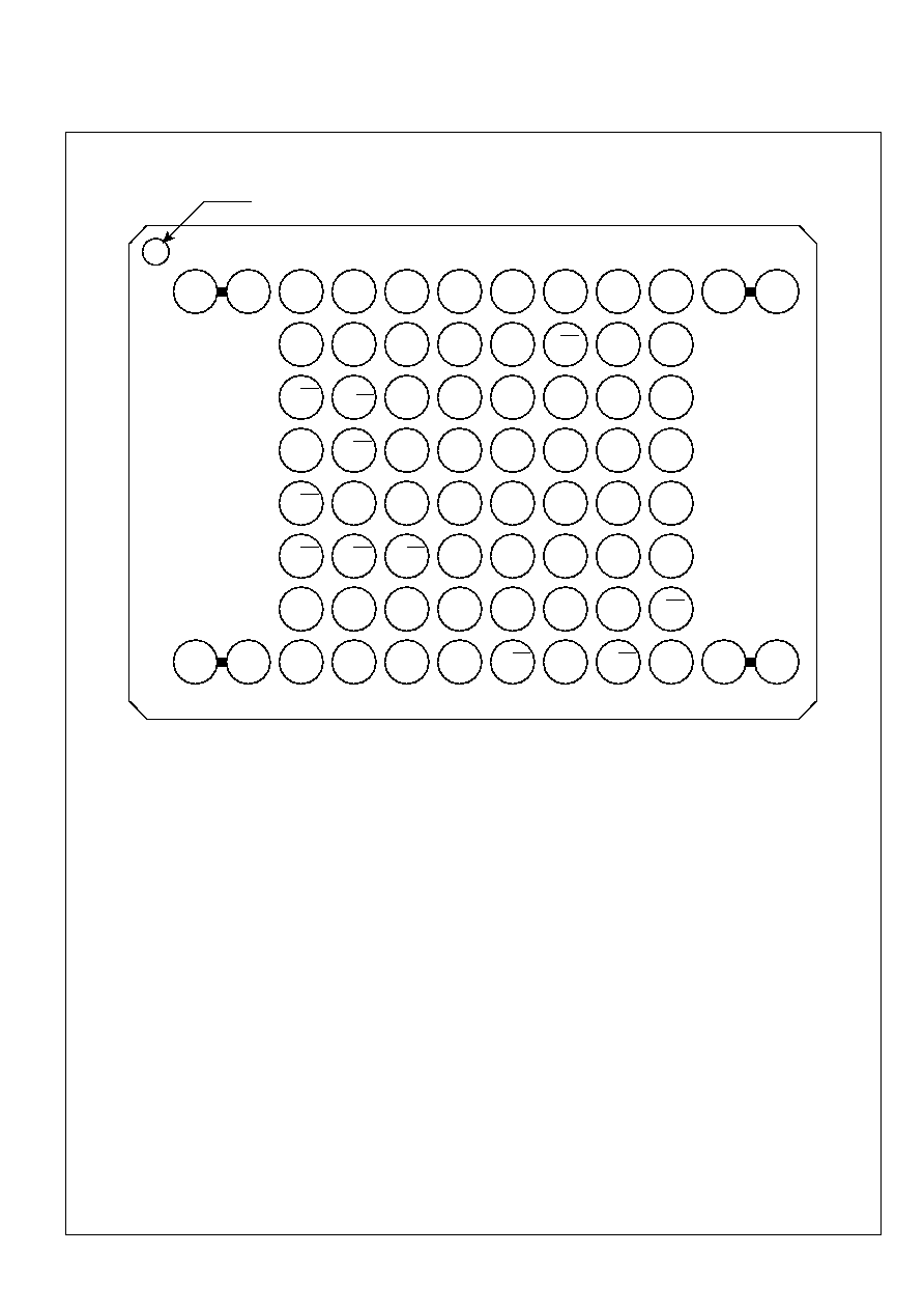
2. Pin Configuration . . . . . . . . . . . . . . . . . . . . . . . . . . . . . . . . . . . . . . . . . . . . . . . . . . . . . . . . . . . . . . . . . . . . . . . . . . . . . . . 3
3. Truth Table . . . . . . . . . . . . . . . . . . . . . . . . . . . . . . . . . . . . . . . . . . . . . . . . . . . . . . . . . . . . . . . . . . . . . . . . . . . . . . . . . . . . 5
4. Block Diagram . . . . . . . . . . . . . . . . . . . . . . . . . . . . . . . . . . . . . . . . . . . . . . . . . . . . . . . . . . . . . . . . . . . . . . . . . . . . . . . . . 6
5. Command Definitions for Flash Memory . . . . . . . . . . . . . . . . . . . . . . . . . . . . . . . . . . . . . . . . . . . . . . . . . . . . . . . . . . . . 7
5.1 Command Definitions . . . . . . . . . . . . . . . . . . . . . . . . . . . . . . . . . . . . . . . . . . . . . . . . . . . . . . . . . . . . . . . . . . . . . . 7
5.2. Identifier Codes . . . . . . . . . . . . . . . . . . . . . . . . . . . . . . . . . . . . . . . . . . . . . . . . . . . . . . . . . . . . . . . . . . . . . . . . . . 8
5.3. Write Protection Alternatives . . . . . . . . . . . . . . . . . . . . . . . . . . . . . . . . . . . . . . . . . . . . . . . . . . . . . . . . . . . . . . . . 8
6. Status Register Definition. . . . . . . . . . . . . . . . . . . . . . . . . . . . . . . . . . . . . . . . . . . . . . . . . . . . . . . . . . . . . . . . . . . . . . . . 9
7. Memory Map for Flash Memory . . . . . . . . . . . . . . . . . . . . . . . . . . . . . . . . . . . . . . . . . . . . . . . . . . . . . . . . . . . . . . . . . . 10
8. Absolute Maximum Ratings. . . . . . . . . . . . . . . . . . . . . . . . . . . . . . . . . . . . . . . . . . . . . . . . . . . . . . . . . . . . . . . . . . . . . . 11
9. Recommended DC Operating Conditions . . . . . . . . . . . . . . . . . . . . . . . . . . . . . . . . . . . . . . . . . . . . . . . . . . . . . . . . . . . 11
10. Pin Capacitance . . . . . . . . . . . . . . . . . . . . . . . . . . . . . . . . . . . . . . . . . . . . . . . . . . . . . . . . . . . . . . . . . . . . . . . . . . . . . . . 11
11. DC Electrical Characteristics . . . . . . . . . . . . . . . . . . . . . . . . . . . . . . . . . . . . . . . . . . . . . . . . . . . . . . . . . . . . . . . . . . . . . 12
12. AC Electrical Characteristics for Flash Memory . . . . . . . . . . . . . . . . . . . . . . . . . . . . . . . . . . . . . . . . . . . . . . . . . . . . . . 14
12.1 AC Test Conditions. . . . . . . . . . . . . . . . . . . . . . . . . . . . . . . . . . . . . . . . . . . . . . . . . . . . . . . . . . . . . . . . . . . . . . . 14
12.2 Read Cycle . . . . . . . . . . . . . . . . . . . . . . . . . . . . . . . . . . . . . . . . . . . . . . . . . . . . . . . . . . . . . . . . . . . . . . . . . . . . . 14
12.3 Write Cycle (F-WE Controlled) . . . . . . . . . . . . . . . . . . . . . . . . . . . . . . . . . . . . . . . . . . . . . . . . . . . . . . . . . . . . . 15
12.4 Write Cycle (F-CE Controlled). . . . . . . . . . . . . . . . . . . . . . . . . . . . . . . . . . . . . . . . . . . . . . . . . . . . . . . . . . . . . . 16
12.5 Block Erase, Full Chip Erase, Word Write and Lock-Bits Configuration Performance . . . . . . . . . . . . . . . . . . 17
12.6 Flash Memory AC Characteristics Timing Chart . . . . . . . . . . . . . . . . . . . . . . . . . . . . . . . . . . . . . . . . . . . . . . . . 18
12.7 Reset Operations . . . . . . . . . . . . . . . . . . . . . . . . . . . . . . . . . . . . . . . . . . . . . . . . . . . . . . . . . . . . . . . . . . . . . . . . . 21
13. AC Electrical Characteristics for SRAM . . . . . . . . . . . . . . . . . . . . . . . . . . . . . . . . . . . . . . . . . . . . . . . . . . . . . . . . . . . . 22
13.1 AC Test Conditions. . . . . . . . . . . . . . . . . . . . . . . . . . . . . . . . . . . . . . . . . . . . . . . . . . . . . . . . . . . . . . . . . . . . . . . 22
13.2 Read Cycle . . . . . . . . . . . . . . . . . . . . . . . . . . . . . . . . . . . . . . . . . . . . . . . . . . . . . . . . . . . . . . . . . . . . . . . . . . . . . 22
13.3 Write Cycle . . . . . . . . . . . . . . . . . . . . . . . . . . . . . . . . . . . . . . . . . . . . . . . . . . . . . . . . . . . . . . . . . . . . . . . . . . . . . 23
13.4 SRAM AC Characteristics Timing Chart . . . . . . . . . . . . . . . . . . . . . . . . . . . . . . . . . . . . . . . . . . . . . . . . . . . . . . 24
14. Data Retention Characteristics for SRAM . . . . . . . . . . . . . . . . . . . . . . . . . . . . . . . . . . . . . . . . . . . . . . . . . . . . . . . . . . . 27
15. Notes. . . . . . . . . . . . . . . . . . . . . . . . . . . . . . . . . . . . . . . . . . . . . . . . . . . . . . . . . . . . . . . . . . . . . . . . . . . . . . . . . . . . . . . . 28
16. Flash Memory Data Protection. . . . . . . . . . . . . . . . . . . . . . . . . . . . . . . . . . . . . . . . . . . . . . . . . . . . . . . . . . . . . . . . . . . . 29
17. Design Considerations . . . . . . . . . . . . . . . . . . . . . . . . . . . . . . . . . . . . . . . . . . . . . . . . . . . . . . . . . . . . . . . . . . . . . . . . . . 30
18. Related Document Information . . . . . . . . . . . . . . . . . . . . . . . . . . . . . . . . . . . . . . . . . . . . . . . . . . . . . . . . . . . . . . . . . . . 30
19. Package and Packing Specification . . . . . . . . . . . . . . . . . . . . . . . . . . . . . . . . . . . . . . . . . . . . . . . . . . . . . . . . . . . . . . . . 31
sharp

LR S1348B
Rev. 1.00
2
1. Description
The LRS1348B is a combination memory organized as 1,048,576
×
16 bit flash memory and 262,144
×
16 bit static RAM in one
package.
Features
- Power supply
· · · ·
2.7V to 3.6V(Flash)
· · · ·
2.7V to 3.3V(SRAM)
- Operating temperature
· · · ·
-25°C to +85°C
- Not designed or rated as radiation hardened
- 72 pin CSP (LCSP072-P-0811) plastic package
- Flash memory has P-type bulk silicon, and SRAM has P-type bulk silicon
Flash Memory
- Access Time
· · · ·
90 ns
(Max.)
- Power Supply current (The current for F-V
CC
pin and F-V
CCW
pin)
Read
· · · ·
25 mA
(Max. t
CYCLE
= 200ns, CMOS Input)
Word write
· · · ·
57 mA
(Max.)
Block erase
· · · ·
42 mA
(Max.)
Reset Power-Down
· · · ·
20µA
(Max. F-RP = GND ± 0.2V,
I
OUT
(F-RY/BY) = 0mA)
Standby
· · · ·
30µA
(Max. F-CE = F-RP = F-V
CC
± 0.2V)
- Optimized Array Blocking Architecture
Two 4k-word Boot Blocks
Six 4k-word Parameter Blocks
Thirty-one 32k-word Main Blocks
Top Boot Location
- Extended Cycling Capability
100,000 Block Erase Cycles
(F-V
CCW
= 2.7 to 3.6V)
- Enhanced Automated Suspend Options
Word Write Suspend to Read
Block Erase Suspend to Word Write
Block Erase Suspend to Read
SRAM
- Access Time
· · · ·
85 ns
(Max.)
- Power Supply current
Operating current
· · · ·
8 mA
(Max. t
RC
,t
WC
= 1µs, CMOS Input)
Standby current
· · · ·
15µA
(Max.)
Data retention current
· · · ·
15µA
(Max. S-V
CC
= 3.0V)
sharp