 | –≠–ª–µ–∫—Ç—Ä–æ–Ω–Ω—ã–π –∫–æ–º–ø–æ–Ω–µ–Ω—Ç: LRS1361F | –°–∫–∞—á–∞—Ç—å:  PDF PDF  ZIP ZIP |

Æ
Integrated Circuits Group
LRS1361F
Stacked Chip
32M (x16) Flash and 4M (x16) SRAM
(Model No.:
LRS1361F)
Spec No.:
EL131010
Issue Date:
July 19, 2001
P
RODUCT
S
PECIFICATIONS

L R S 1 3 6 1 F
∑ Handle this document carefully for it contains material protected by international copyright law.
Any reproduction, full or in part, of this material is prohibited without the express written permission
of the company.
∑ When using the products covered herein, please observe the conditions written herein and the
precautions outlined in the following paragraphs. In no event shall the company be liable for
any damages resulting from failure to strictly adhere to these conditions and precautions.
(1) The products covered herein are designed and manufactured for the following application areas.
When using the products covered herein for the equipment listed in Paragraph (2), even for the
following application areas, be sure to observe the precautions given in Paragraph (2). Never use
the products for the equipment listed in Paragraph (3).
∑ Office electronics
∑ Instrumentation and measuring equipment
∑ Machine tools
∑ Audiovisual equipment
∑ Home appliance
∑ Communication equipment other than for trunk lines
(2) Those contemplating using the products covered herein for the following equipment
which demands high reliability, should first contact a sales representative of the company and
then accept responsibility for incorporating into the design fail-safe operation, redundancy, and
other appropriate measures for ensuring reliability and safety of the equipment and the overall
system.
∑ Control and safety devices for airplanes, trains, automobiles, and other transportation
equipment
∑ Mainframe computers
∑ Traffic control systems
∑ Gas leak detectors and automatic cutoff devices
∑ Rescue and security equipment
∑ Other safety devices and safety equipment, etc.
(3) Do not use the products covered herein for the following equipment which demands extremely
high performance in terms of functionality, reliability, or accuracy.
∑ Aerospace equipment
∑ Communications equipment for trunk lines
∑ Control equipment for the nuclear power industry
∑ Medical equipment related to life support, etc.
(4) Please direct all queries and comments regarding the interpretation of the above three
Paragraphs to a sales representative of the company.
∑ Please direct all queries regarding the products covered herein to a sales representative of the
company.
sharp

L R S 1 3 6 1 F
1
Contents
1. Description. . . . . . . . . . . . . . . . . . . . . . . . . . . . . . . . . . . . . . . . . . . . . . . . . . . . . . . . . . . . . . . . . . . . . . . . . . . . . . . . . . . . . 2
2. Pin Configuration. . . . . . . . . . . . . . . . . . . . . . . . . . . . . . . . . . . . . . . . . . . . . . . . . . . . . . . . . . . . . . . . . . . . . . . . . . . . . . . . 3
3. Truth Table . . . . . . . . . . . . . . . . . . . . . . . . . . . . . . . . . . . . . . . . . . . . . . . . . . . . . . . . . . . . . . . . . . . . . . . . . . . . . . . . . . . . 5
4. Block Diagram. . . . . . . . . . . . . . . . . . . . . . . . . . . . . . . . . . . . . . . . . . . . . . . . . . . . . . . . . . . . . . . . . . . . . . . . . . . . . . . . . . 6
5. Command Definitions for Flash Memory . . . . . . . . . . . . . . . . . . . . . . . . . . . . . . . . . . . . . . . . . . . . . . . . . . . . . . . . . . . . . 7
5.1
Command Definitions . . . . . . . . . . . . . . . . . . . . . . . . . . . . . . . . . . . . . . . . . . . . . . . . . . . . . . . . . . . . . . . . . . . . . . 7
5.2
Identifier Codes . . . . . . . . . . . . . . . . . . . . . . . . . . . . . . . . . . . . . . . . . . . . . . . . . . . . . . . . . . . . . . . . . . . . . . . . . . . 8
5.3
OTP Block Address Map . . . . . . . . . . . . . . . . . . . . . . . . . . . . . . . . . . . . . . . . . . . . . . . . . . . . . . . . . . . . . . . . . . . . 8
5.4
Write Protection Alternatives. . . . . . . . . . . . . . . . . . . . . . . . . . . . . . . . . . . . . . . . . . . . . . . . . . . . . . . . . . . . . . . . . 9
6. Status Register Definition . . . . . . . . . . . . . . . . . . . . . . . . . . . . . . . . . . . . . . . . . . . . . . . . . . . . . . . . . . . . . . . . . . . . . . . . 10
7. Memory Map for Flash Memory . . . . . . . . . . . . . . . . . . . . . . . . . . . . . . . . . . . . . . . . . . . . . . . . . . . . . . . . . . . . . . . . . . . 11
8. Absolute Maximum Ratings . . . . . . . . . . . . . . . . . . . . . . . . . . . . . . . . . . . . . . . . . . . . . . . . . . . . . . . . . . . . . . . . . . . . . . 12
9. Recommended DC Operating Conditions . . . . . . . . . . . . . . . . . . . . . . . . . . . . . . . . . . . . . . . . . . . . . . . . . . . . . . . . . . . . 12
10. Pin Capacitance . . . . . . . . . . . . . . . . . . . . . . . . . . . . . . . . . . . . . . . . . . . . . . . . . . . . . . . . . . . . . . . . . . . . . . . . . . . . . . . 12
11. DC Electrical Characteristics . . . . . . . . . . . . . . . . . . . . . . . . . . . . . . . . . . . . . . . . . . . . . . . . . . . . . . . . . . . . . . . . . . . . . 13
12. AC Electrical Characteristics for Flash Memory . . . . . . . . . . . . . . . . . . . . . . . . . . . . . . . . . . . . . . . . . . . . . . . . . . . . . . 15
12.1 AC Test Conditions . . . . . . . . . . . . . . . . . . . . . . . . . . . . . . . . . . . . . . . . . . . . . . . . . . . . . . . . . . . . . . . . . . . . . . . 15
12.2 Read Cycle . . . . . . . . . . . . . . . . . . . . . . . . . . . . . . . . . . . . . . . . . . . . . . . . . . . . . . . . . . . . . . . . . . . . . . . . . . . . . . 15
12.3 Write Cycle (F-WE Controlled) . . . . . . . . . . . . . . . . . . . . . . . . . . . . . . . . . . . . . . . . . . . . . . . . . . . . . . . . . . . . . . 16
12.4 Write Cycle (F-CE Controlled) . . . . . . . . . . . . . . . . . . . . . . . . . . . . . . . . . . . . . . . . . . . . . . . . . . . . . . . . . . . . . . 17
12.5 Block Erase, Full Chip Erase, Word Write and Lock-Bits Configuration Performance . . . . . . . . . . . . . . . . . . . 18
12.6 Flash Memory AC Characteristics Timing Chart . . . . . . . . . . . . . . . . . . . . . . . . . . . . . . . . . . . . . . . . . . . . . . . . 19
12.7 Reset Operations . . . . . . . . . . . . . . . . . . . . . . . . . . . . . . . . . . . . . . . . . . . . . . . . . . . . . . . . . . . . . . . . . . . . . . . . . 22
13. AC Electrical Characteristics for SRAM . . . . . . . . . . . . . . . . . . . . . . . . . . . . . . . . . . . . . . . . . . . . . . . . . . . . . . . . . . . . 23
13.1 AC Test Conditions . . . . . . . . . . . . . . . . . . . . . . . . . . . . . . . . . . . . . . . . . . . . . . . . . . . . . . . . . . . . . . . . . . . . . . . 23
13.2 Read Cycle . . . . . . . . . . . . . . . . . . . . . . . . . . . . . . . . . . . . . . . . . . . . . . . . . . . . . . . . . . . . . . . . . . . . . . . . . . . . . . 23
13.3 Write Cycle . . . . . . . . . . . . . . . . . . . . . . . . . . . . . . . . . . . . . . . . . . . . . . . . . . . . . . . . . . . . . . . . . . . . . . . . . . . . . 24
13.4 SRAM AC Characteristics Timing Chart. . . . . . . . . . . . . . . . . . . . . . . . . . . . . . . . . . . . . . . . . . . . . . . . . . . . . . . 25
14. Data Retention Characteristics for SRAM . . . . . . . . . . . . . . . . . . . . . . . . . . . . . . . . . . . . . . . . . . . . . . . . . . . . . . . . . . . 29
15. Notes . . . . . . . . . . . . . . . . . . . . . . . . . . . . . . . . . . . . . . . . . . . . . . . . . . . . . . . . . . . . . . . . . . . . . . . . . . . . . . . . . . . . . . . 30
16. Flash Memory Data Protection . . . . . . . . . . . . . . . . . . . . . . . . . . . . . . . . . . . . . . . . . . . . . . . . . . . . . . . . . . . . . . . . . . . 31
17. Design Considerations . . . . . . . . . . . . . . . . . . . . . . . . . . . . . . . . . . . . . . . . . . . . . . . . . . . . . . . . . . . . . . . . . . . . . . . . . . 32
18. Related Document Information . . . . . . . . . . . . . . . . . . . . . . . . . . . . . . . . . . . . . . . . . . . . . . . . . . . . . . . . . . . . . . . . . . . 32
19. Package and Packing Specification . . . . . . . . . . . . . . . . . . . . . . . . . . . . . . . . . . . . . . . . . . . . . . . . . . . . . . . . . . . . . . . . 33
sharp

L R S 1 3 6 1 F
2
1. Description
The LRS1361F is a combination memory organized as 2,097,152
◊ 16 bit flash memory and 262,144 ◊ 16 bit static RAM in one
package.
Features
- Power supply
∑ ∑ ∑ ∑
2.7V to 3.3V
- Operating temperature
∑ ∑ ∑ ∑
-25∞C to +85∞C
- Not designed or rated as radiation hardened
- 72pin CSP(LCSP072-P-0811) plastic package
- Flash memory has P-type bulk silicon, and SRAM has P-type bulk silicon
Flash Memory
- Access Time
∑ ∑ ∑ ∑
90 ns
(Max.)
- Power supply current (The current for F-V
CC
pin and F-V
CCW
pin)
Read
∑ ∑ ∑ ∑
25 mA
(Max. t
CYCLE
= 200ns, CMOS Input)
Word write
∑ ∑ ∑ ∑
57 mA
(Max.)
Block erase
∑ ∑ ∑ ∑
42 mA
(Max.)
Reset Power-Down
∑ ∑ ∑ ∑
25 µA
(Max. F-RP = GND ± 0.2V,
I
OUT
(F-RY/BY) = 0mA)
Standby
∑ ∑ ∑ ∑
35 µA
(Max. F-CE = F-RP = F-V
CC
± 0.2V)
- Optimized Array Blocking Architecture
Two 4K-word Boot Blocks
Six 4K-word Parameter Blocks
Sixty-Three 32K-word Main Blocks
Bottom Boot Location
- Extended Cycling Capability
100,000 Block Erase Cycles
(F-V
CCW
= 2.7V to 3.3V)
1,000 Block Erase Cycles and total 80 hours (F-V
CCW
= 11.7V to 12.3V)
- Enhanced Automated Suspend Options
Word Write Suspend to Read
Block Erase Suspend to Word Write
Block Erase Suspend to Read
- OTP Block
3963 Word + 4 Word Array
SRAM
- Access Time
∑ ∑ ∑ ∑
85 ns
(Max.)
- Power Supply current
Operating current
∑ ∑ ∑ ∑
45 mA
(Max. t
RC
, t
WC
= Min.)
∑ ∑ ∑ ∑
8 mA
(Max. t
RC
, t
WC
= 1µs, CMOS Input)
Standby current
∑ ∑ ∑ ∑
15 µA
(Max.)
Data retention current
∑ ∑ ∑ ∑
15 µA
(Max. S-V
CC
= 3.0V)
sharp

L R S 1 3 6 1 F
3
2. Pin Configuration
NC
NC
F-A
20
A
16
A
11
A
8
A
10
A
15
A
14
A
9
DQ
15
A
13
A
12
1
2
3
4
5
6
7
8
S-WE
F-WE
F-
RY/BY
F-RP
T
2
T
1
S-A
17
T
4
DQ
12
GND
DQ
13
DQ
6
S-CE
2
F-WP
S-LB S-UB S-OE
F-A
19
DQ
11
NC
DQ
9
T
3
DQ
10
DQ
8
A
B
C
D
E
F
G
F-A
18
F-A
17
A
7
A
6
A
3
A
2
GND
9
DQ
14
DQ
4
S-V
CC
DQ
2
DQ
0
A
1
NC
10
DQ
7
DQ
5
F-V
CC
DQ
3
DQ
1
S-CE
1
NC
11
NC
12
NC
H
NC
NC
A
5
A
4
A
0
F-CE
GND
F-OE
NC
NC
NC
Note) From T
1
to T
4
pins are needed to be open.
Two NC pins at the corner are connected.
Do not float any GND pins.
INDEX
(TOP View)
F-V
CCW
sharp
L R S 1 3 6 1 F
4
Pin
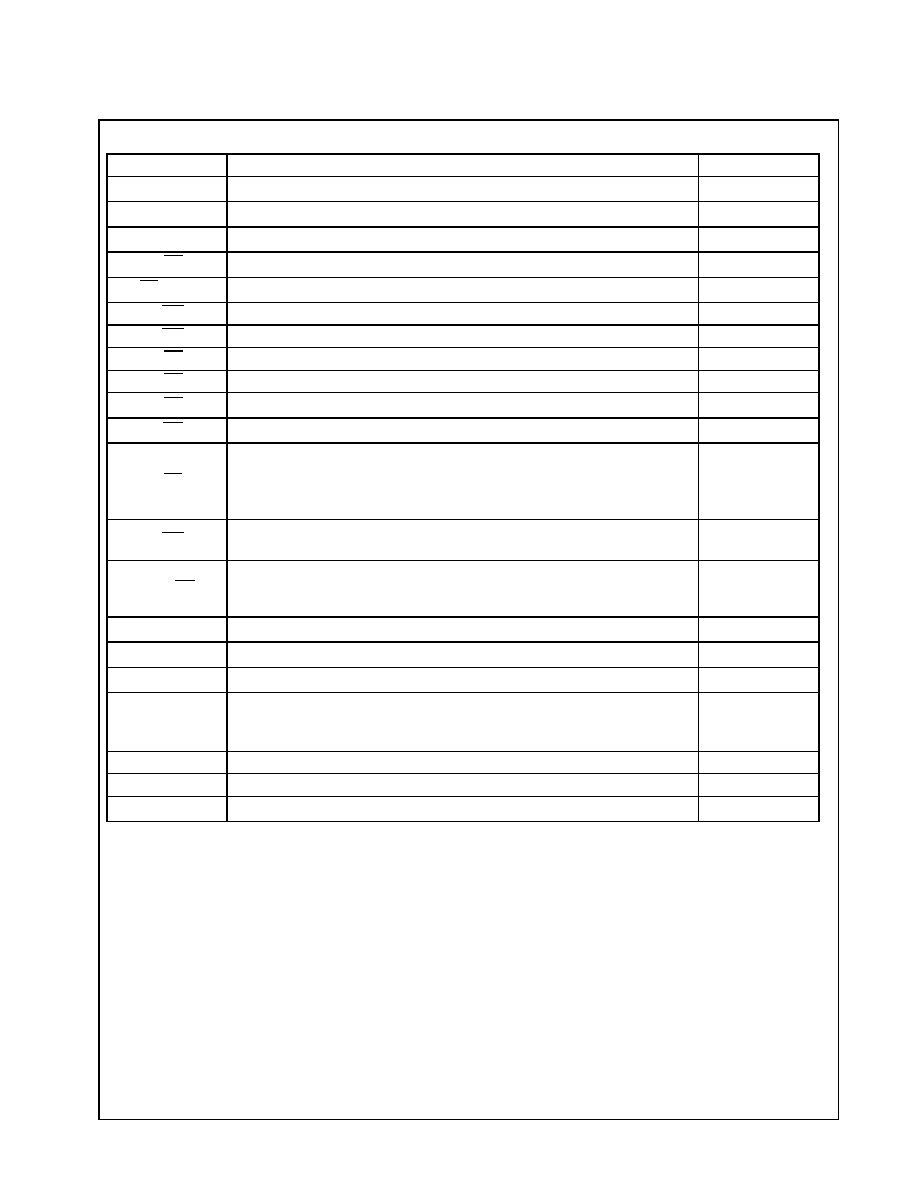
Description
Type
A
0
to A
16
Address Inputs (Common)
Input
F-A
17
to F-A
20
Address Inputs (Flash)
Input
S-A
17
Address Input (SRAM)
Input
F-CE
Chip Enable Inputs (Flash)
Input
S-CE
1
, S-CE
2
Chip Enable Inputs (SRAM)
Input
F-WE
Write Enable Input (Flash)
Input
S-WE
Write Enable Input (SRAM)
Input
F-OE
Output Enable Input (Flash)
Input
S-OE
Output Enable Input (SRAM)
Input
S-LB
SRAM Byte Enable Input (DQ
0
to DQ
7
)
Input
S-UB
SRAM Byte Enable Input (DQ
8
to DQ
15
)
Input
F-RP
Reset Power Down Input (Flash)
Block erase and Write : V
IH
Read : V
IH
Reset Power Down : V
IL
Input
F-WP
Write Protect Input (Flash)
Two Boot Blocks Locked : V
IL
Input
F-RY/BY
Ready/Busy Output (Flash)
During an Erase or Write operation : V
OL
Block Erase and Write Suspend : High-Z (High impedance)
Open Drain
Output
DQ
0
to DQ
15
Data Inputs and Outputs (Common)
Input / Output
F-V
CC
Power Supply (Flash)
Power
S-V
CC
Power Supply (SRAM)
Power
F-V
CCW
Write, Erase Power Supply (Flash)
Block Erase and Write : F-V
CCW =
V
CCWH1/2
All Blocks Locked : F-V
CCW
< V
CCWLK
Power
GND
GND (Common)
Power
NC
Non Connection (Should be all open)
-
T
1
to T
4
Test pins (Should be all open)
-
sharp
L R S 1 3 6 1 F
5
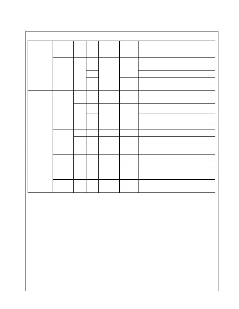
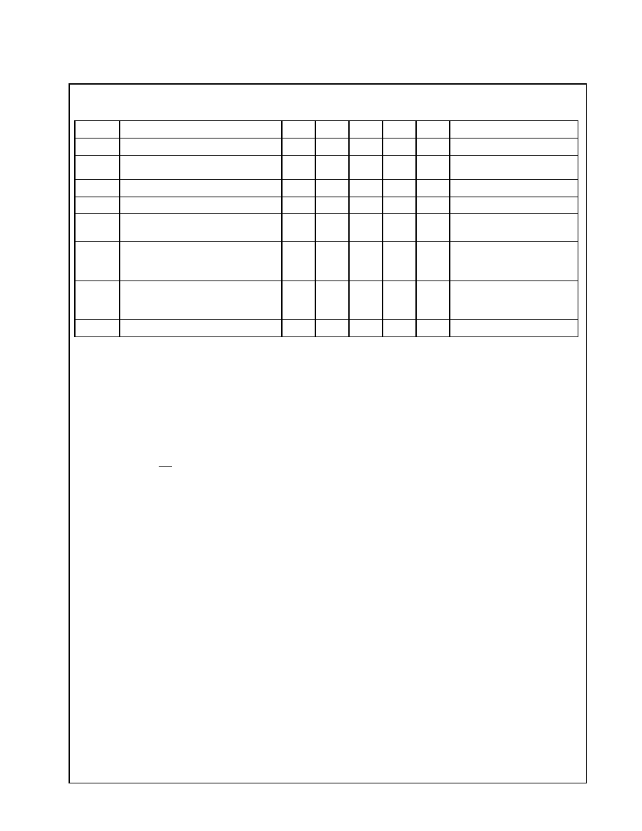
3. Truth Table
(1)
Notes:
1. L = V
IL
, H = V
IH
, X = H or L. Refer to DC Characteristics. High-Z = High impedance.
2. Command writes involving block erase, full chip erase, word write, OTP write or lock-bit configuration are reliably
executed when F-V
CCW
= V
CCWH1/2
and F-V
CC
= 2.7V to 3.3V.
Block erase, full chip erase, word write, OTP write or lock-bit configuration with F-V
CCW
< V
CCWH1/2
(Min.) produce
spurious results and should not be attempted.
3. Never hold F-OE low and F-WE low at the same timing.
4. Refer Section 5. Command Definitions for Flash Memory valid D
IN
during a write operation.
5. F-WP set to V
IL or
V
IH
.
6. SRAM Standby Mode
7. S-UB, S-LB Control Mode
Flash
SRAM
Notes
F-CE
F-RP
F-OE F-WE S-CE
1
S-CE
2
S-OE S-WE S-LB S-UB DQ
0
to DQ
15
Read
Standby
3,5
L
H
L
H
(6)
X
X
(6)
D
OUT
Output
Disable
5
H
High-Z
Write
2,3,4,5
L
D
IN
Standby
Read
5
H
H
X
X
L
H
L
H
(7)
Output
Disable
5
H
H
X
X
High-Z
X
X
H
H
Write
5
X
L
(7)
Reset Power
Down
Read
5
X
L
X
X
L
H
L
H
(7)
Output
Disable
5
H
H
X
X
High-Z
X
X
H
H
Write
5
X
L
(7)
Standby
Standby
5
H
H
X
X
(6)
X
X
(6)
High-Z
Reset Power
Down
5
X
L
S-CE
1
S-CE
2
S-LB
S-UB
S-LB
S-UB
DQ
0
to DQ
7
DQ
8
to DQ
15
H
X
X
X
L
L
D
OUT
/D
IN
D
OUT
/D
IN
X
L
X
X
L
H
D
OUT
/D
IN
High-Z
X
X
H
H
H
L
High-Z
D
OUT
/D
IN
sharp
L R S 1 3 6 1 F
6
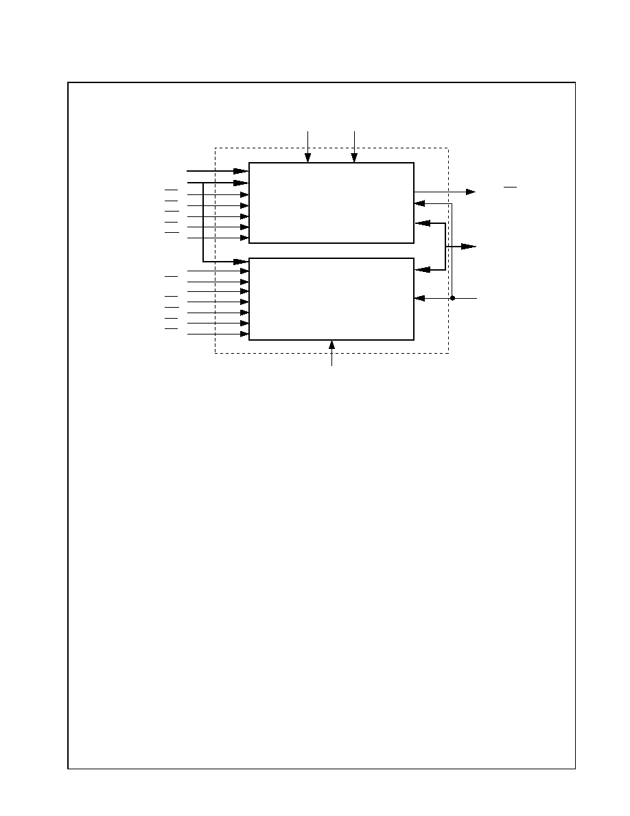
4. Block Diagram
S-V
CC
32M (x16) bit
Flash memory
4M (x16) bit
SRAM
S-A
17
S-CE
1
S-CE
2
S-OE
S-WE
S-LB
S-UB
F-V
CCW
F-V
CC
F-CE
A
0
to A
16
DQ
0
to DQ
15
F-A
17
to F-A
20
F-OE
F-WE
F-WP
F-RP
F-RY/BY
GND
sharp
L R S 1 3 6 1 F
7
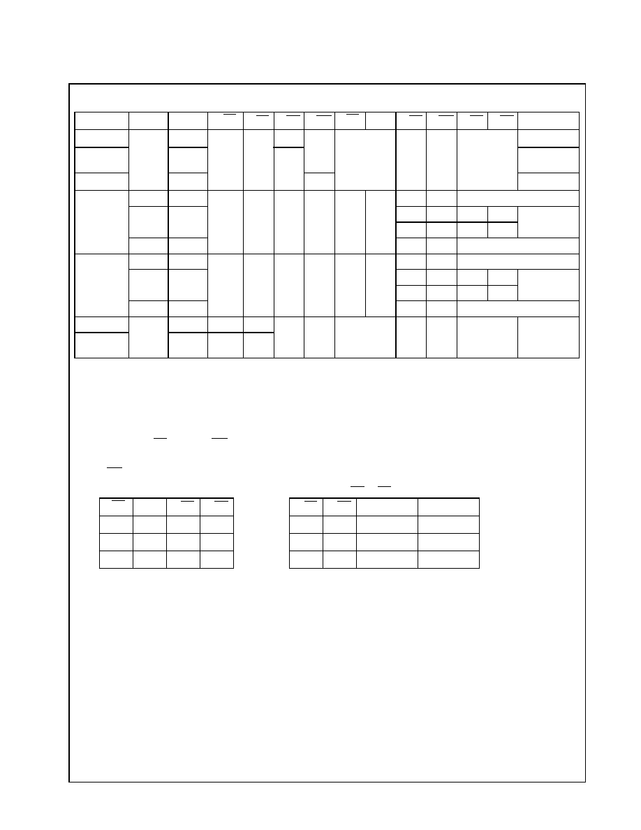
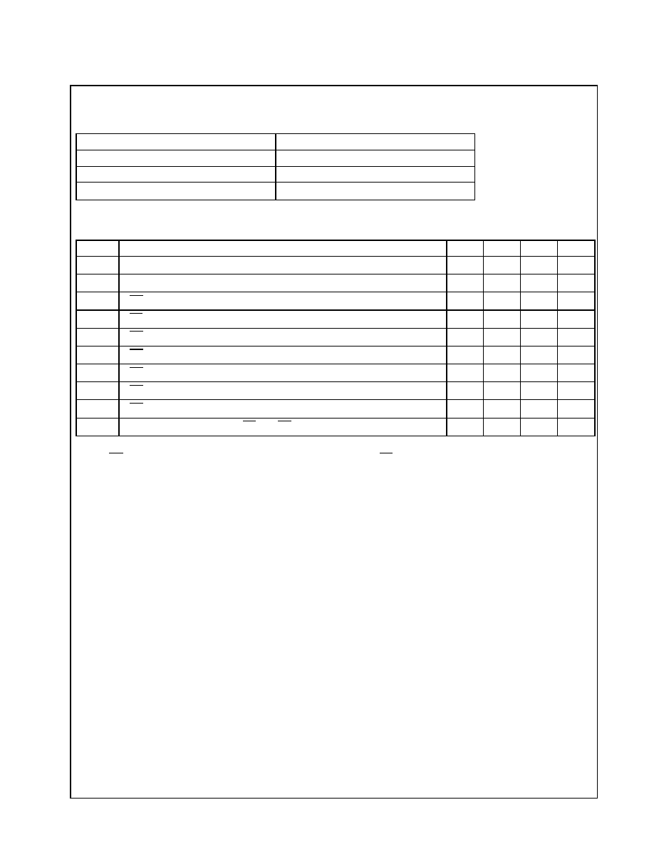
5. Command Definitions for Flash Memory
(1)
5.1 Command Definitions
Notes:
1. Commands other than those shown above are reserved by SHARP for future device implementations and should not be used.
2. Bus operations are defined in 3. Truth Table.
3. XA = Any valid address within the device.
IA = Identifier code address.
BA = Address within the block being erased.
WA = Address of memory location to be written.
SRD = Data read from status register (See 6. Status Register Definition).
WD = Data to be written at location WA. Data is latched on the rising edge of F-WE or F-CE (whichever goes high first).
ID = Data read from identifier codes (See 5.2 Identifier Codes).
OA = OTP Address.
OD = Data to be written at location OA. Data is latched on the rising edge of F-WE or F-CE (whichever goes high first).
4. Following the Read Identifier Codes/OTP command, read operations access manufacturer, device, block lock
configuration codes and data within OTP block.
5. See Write Protection Alternatives in section 5.4.
6. The clear block lock-bits operation simultaneously clears all block lock-bits.
7. If the permanent lock-bit is set, Set Block Lock-Bit and Clear Block Lock-Bits commands can not be done.
8. Once the permanent lock-bit is set, it cannot be cleared.
9. If the time between writing the Block Erase Resume command and writing the Block Erase Suspend command is shorter
than t
ERES
and both commands are written repeatedly, a longer time is required than standard block erase until the
completion of the operation.
Command
Bus Cycles
Required
Note
First Bus Cycle
Second Bus Cycle
Oper
(2)
Address
(3)
Data
Oper
(2)
Address
(3)
Data
(3)
Read Array / Reset
1
Write
XA
FFH
Read Identifier Codes / OTP
2
4
Write
XA
90H
Read
IA ID
Read Status Register
2
Write
XA
70H
Read
XA
SRD
Clear Status Register
1
Write
XA
50H
Block Erase
2
5
Write
XA
20H
Write
BA
D0H
Full Chip Erase
2
5
Write
XA
30H
Write
XA
D0H
Word Write
2
5
Write
XA
40H or
10H
Write
WA
WD
Block Erase and Word Write
Suspend
1
5,9
Write
XA
B0H
Block Erase and Word Write
Resume
1
5,9
Write
XA
D0H
Set Block Lock-Bit
2
7
Write
XA
60H
Write
BA
01H
Clear Block Lock-Bits
2
6,7
Write
XA
60H
Write
XA
D0H
Set Permanent Lock-Bit
2
8
Write
XA
60H
Write
XA
F1H
OTP Write
2
Write
XA
C0H
Write
OA
OD
sharp

L R S 1 3 6 1 F
8
5.2 Identifier Codes
(3)
Notes:
1. BA selects the specific block lock configuration code to be read.
2. DQ
15
to DQ
1
are reserved for future use.
3. Read Identifier Codes command is defined in 5.1 Command Definitions.
5.3 OTP Block Address Map
Codes
Address [A
20
to A
0
]
Data [DQ
15
to DQ
0
]
Manufacture Code
00000H
00B0H
Device Code
00001H
00E3H
Block Lock Configuration
(2)
BA
(1)
+2
DQ
0
= 0 : Unlocked
DQ
0
= 1 : Locked
Permanent Lock Configuration
(2)
00003H
DQ
0
= 0 : Unlocked
DQ
0
= 1 : Locked
Customer Program Area Lock Bit
Factory Program Area Lock Bit
OTP Block Address Map for OTP Program
(The area below 80H cannot be used.)
Customer Program Area
Factory Program Area
Reserved for Future Implementation
000080
000081
000084
000085
000FFF
[A
20
-A
0
]
sharp
L R S 1 3 6 1 F
9
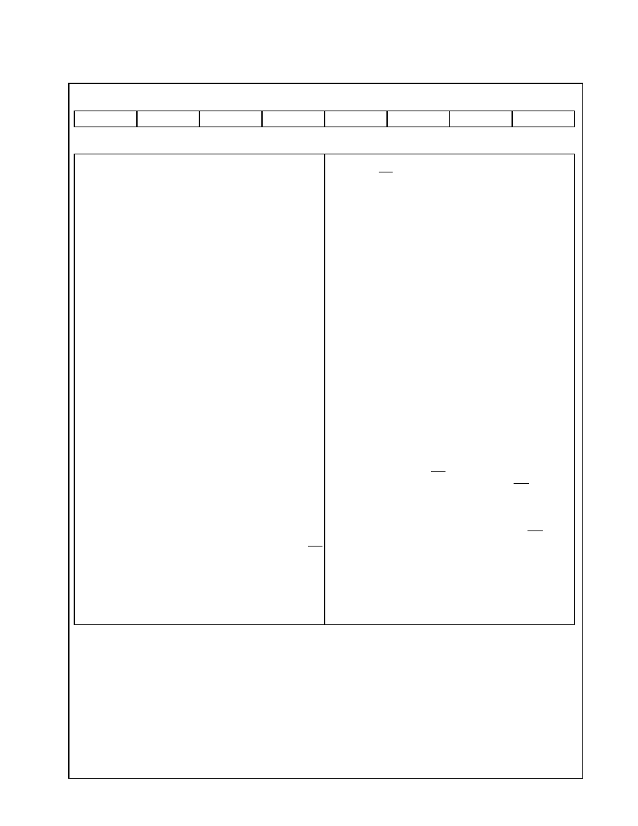
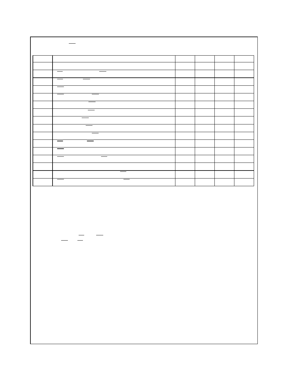
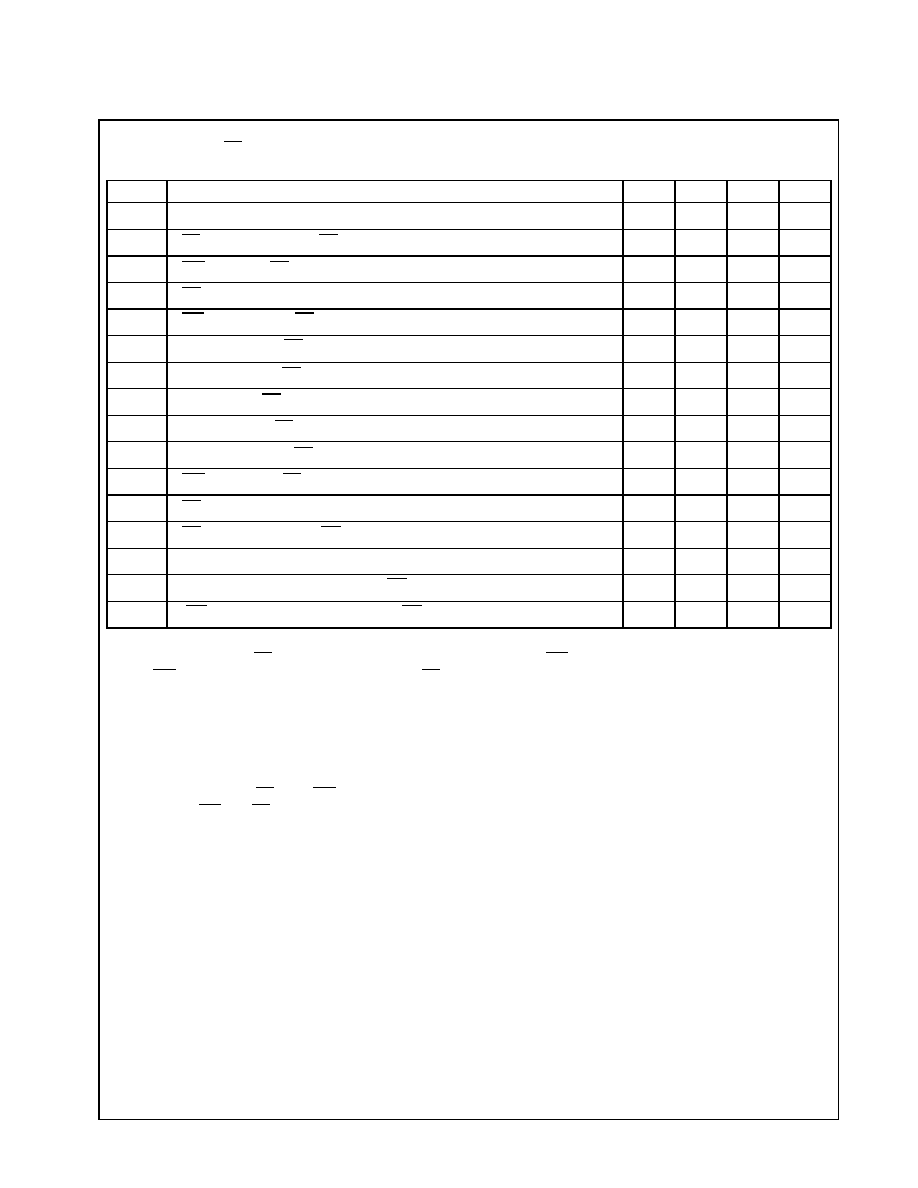
5.4 Write Protection Alternatives
Note:
1. F-V
CCW
is guaranteed only with the nominal voltages.
Operation
F-V
CCW
F-RP
F-WP
Permanent
Lock-Bit
Block
Lock-Bit
Effect
Block Erase or
Word Write
V
CCWLK
X
X
X
X
All Blocks Locked.
>V
CCWLK
(1)
V
IL
X
X
X
All Blocks Locked.
V
IH
V
IL
X
0
2 Boot Blocks Locked.
V
IH
Block Erase and Word Write Enabled.
V
IL
1
Block Erase and Word Write Disabled.
V
IH
Block Erase and Word Write Disabled.
Full Chip Erase
V
CCWLK
X
X
X
X
All Blocks Locked.
>V
CCWLK
(1)
V
IL
X
X
X
All Blocks Locked.
V
IH
V
IL
X
X
All Unlocked Blocks are Erased.
2 Boot Blocks and Locked Blocks are Not Erased.
V
IH
All Unlocked Blocks are Erased.
Locked Blocks are Not Erased.
Set Block
Lock-Bit
V
CCWLK
X
X
X
X
Set Block Lock-Bit Disabled.
>V
CCWLK
(1)
V
IL
X
X
X
Set Block Lock-Bit Disabled.
V
IH
X
0
X
Set Block Lock-Bit Enabled.
X
1
X
Set Block Lock-Bit Disabled.
Clear Block
Lock-Bits
V
CCWLK
X
X
X
X
Clear Block Lock-Bits Disabled.
>V
CCWLK
(1)
V
IL
X
X
X
Clear Block Lock-Bits Disabled.
V
IH
X
0
X
Clear Block Lock-Bits Enabled.
X
1
X
Clear Block Lock-Bits Disabled.
Set Permanent
Lock-Bit
V
CCWLK
X
X
X
X
Set Permanent Lock-Bit Disabled.
>V
CCWLK
(1)
V
IL
X
X
X
Set Permanent Lock-Bit Disabled.
V
IH
X
X
X
Set Permanent Lock- Bit Enabled.
sharp
L R S 1 3 6 1 F
10
6. Status Register Definition
WSMS
BESS
ECBLBS
WWSLBS
VCCWS
WWSS
DPS
R
7
6
5
4
3
2
1
0
SR.7 = WRITE STATE MACHINE STATUS (WSMS)
1 = Ready
0 = Busy
SR.6 = BLOCK ERASE SUSPEND STATUS (BESS)
1 = Block Erase Suspended
0 = Block Erase in Progress/Completed
SR.5 = ERASE AND CLEAR BLOCK LOCK-BITS
STATUS (ECBLBS)
1 = Error in Block Erase, Full Chip Erase or Clear Block
Lock-Bits
0 = Successful Block Erase, Full Chip Erase or Clear
Block Lock-Bits
SR.4 = WORD WRITE AND SET LOCK-BIT
STATUS (WWSLBS)
1 = Error in Word Write or Set Block/Permanent
Lock-Bit
0 = Successful Word Write or Set Block/Permanent
Lock-Bit
SR.3 = F-V
CCW
STATUS (VCCWS)
1 = F-V
CCW
Low Detect, Operation Abort
0 = F-V
CCW
OK
SR.2 = WORD WRITE SUSPEND STATUS (WWSS)
1 = Word Write Suspended
0 = Word Write in Progress/Completed
SR.1 = DEVICE PROTECT STATUS (DPS)
1 = Block Lock-Bit, Permanent Lock-Bit and/or F-WP
Lock Detected, Operation Abort
0 = Unlocked
SR.0 = RESERVED FOR FUTURE ENHANCEMENTS (R)
Notes:
Check F-RY/BY or SR.7 to determine Block Erase, Full Chip
Erase, Word Write, OTP Write or Lock-Bit configuration
completion before check SR.5 or SR.4.
SR.6 - SR.0 are invalid while SR.7 = "0".
If both SR.5 and SR.4 are "1"s after a Block Erase, Full Chip
Erase or Lock-Bit configuration attempt, an improper
command sequence was entered.
SR.3 does not provide a continuous indication of F-V
CCW
level. The WSM (Write State Machine) interrogates and
indicates the F-V
CCW
level only after Block Erase, Full Chip
Erase, Word Write, OTP Write or Lock-Bit Configuration
command sequences. SR.3 is not guaranteed to reports
accurate feedback only when F-V
CCW
V
CCWH1/2
.
SR.1 does not provide a continuous indication of permanent
and block lock-bit and F-WP values. The WSM interrogates
the permanent lock-bit, block lock-bit and F-WP only after
Block Erase, Full Chip Erase, Word Write, OTP Write or
Lock-Bit Configuration command sequences. It informs the
system, depending on the attempted operation, if the block
lock-bit is set, permanent lock-bit is set and/or F-WP is V
IL
.
Reading the block lock and permanent lock configuration
codes after writing the Read Identifier Codes command
indicates permanent and block lock-bit status.
SR.0 is reserved for future use and should be masked out when
polling the status register.
sharp
L R S 1 3 6 1 F
11
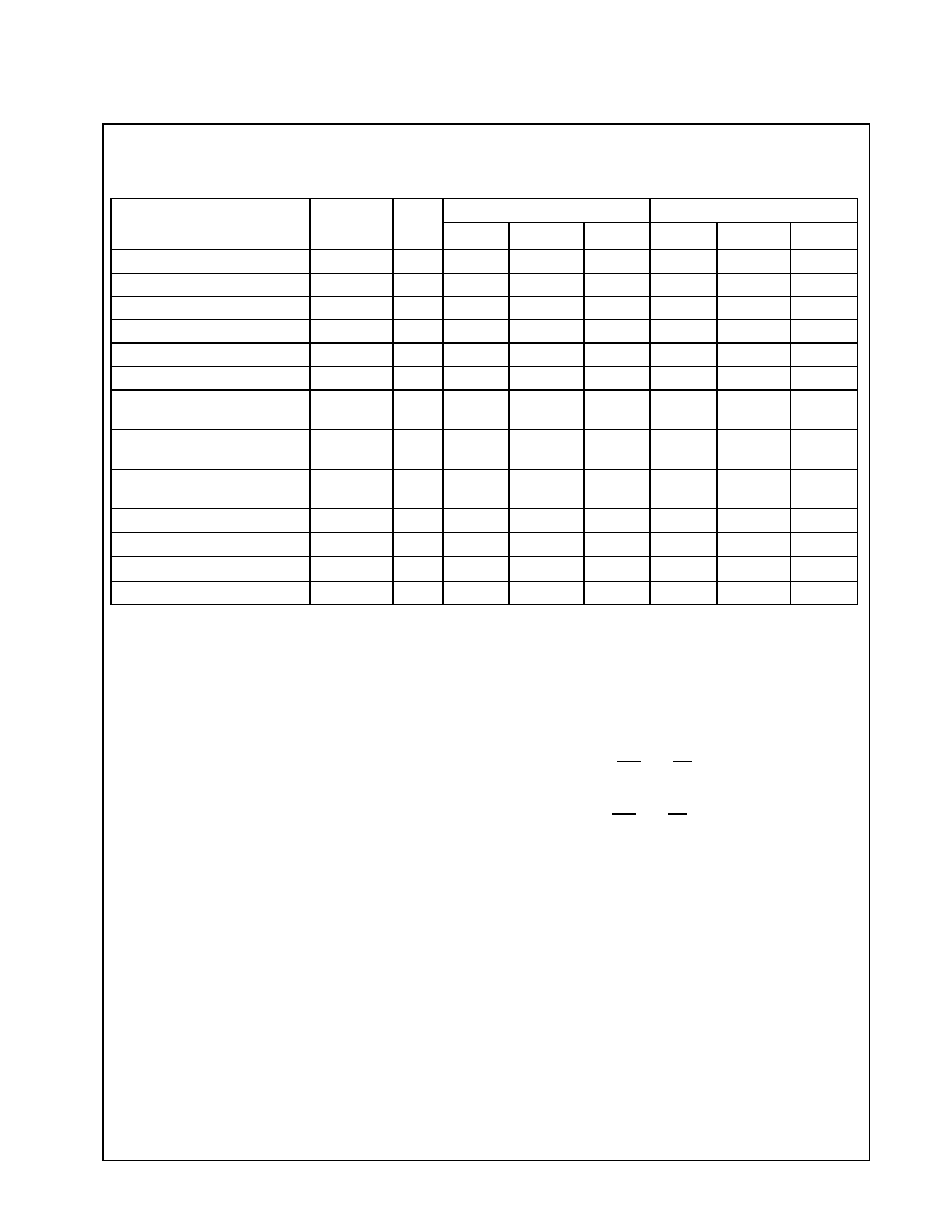
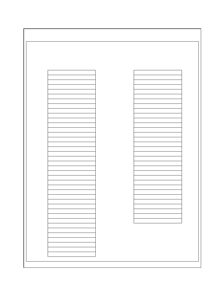
7. Memory Map for Flash Memory
32K-word Main Block 30
32K-word Main Block 29
32K-word Main Block 28
32K-word Main Block 27
32K-word Main Block 26
32K-word Main Block 25
32K-word Main Block 24
32K-word Main Block 23
32K-word Main Block 22
32K-word Main Block 21
32K-word Main Block 20
32K-word Main Block 19
32K-word Main Block 18
32K-word Main Block 17
32K-word Main Block 16
32K-word Main Block 15
32K-word Main Block 14
32K-word Main Block 13
32K-word Main Block 12
32K-word Main Block 11
32K-word Main Block 10
32K-word Main Block 9
32K-word Main Block 8
32K-word Main Block 7
32K-word Main Block 6
32K-word Main Block 5
32K-word Main Block 4
32K-word Main Block 3
32K-word Main Block 2
32K-word Main Block 1
32K-word Main Block 0
4K-word Boot Block 0
4K-word Boot Block 1
4K-word Parameter Block 0
4K-word Parameter Block 1
4K-word Parameter Block 2
4K-word Parameter Block 3
4K-word Parameter Block 4
4K-word Parameter Block 5
32K-word Main Block 61
32K-word Main Block 62
32K-word Main Block 60
32K-word Main Block 59
32K-word Main Block 58
32K-word Main Block 57
32K-word Main Block 56
32K-word Main Block 55
32K-word Main Block 54
32K-word Main Block 53
32K-word Main Block 52
32K-word Main Block 51
32K-word Main Block 50
32K-word Main Block 49
32K-word Main Block 48
32K-word Main Block 47
32K-word Main Block 46
32K-word Main Block 45
32K-word Main Block 44
32K-word Main Block 43
32K-word Main Block 42
32K-word Main Block 41
32K-word Main Block 40
32K-word Main Block 39
32K-word Main Block 38
32K-word Main Block 37
32K-word Main Block 36
32K-word Main Block 35
32K-word Main Block 34
32K-word Main Block 33
32K-word Main Block 32
32K-word Main Block 31
007000
008000
00FFFF
007FFF
006000
006FFF
005000
005FFF
004000
004FFF
003000
003FFF
002000
002FFF
001000
001FFF
000000
000FFF
010000
017FFF
018000
01FFFF
020000
027FFF
028000
02FFFF
030000
037FFF
038000
03FFFF
040000
047FFF
048000
04FFFF
050000
057FFF
058000
05FFFF
060000
067FFF
068000
06FFFF
070000
077FFF
078000
07FFFF
080000
087FFF
088000
08FFFF
090000
097FFF
098000
09FFFF
0A0000
0A7FFF
0A8000
0AFFFF
0B8000
0BFFFF
0C0000
0C7FFF
0C8000
0CFFFF
0D0000
0D7FFF
0D8000
0DFFFF
0E0000
0E7FFF
0E8000
0EFFFF
0F0000
0F7FFF
0F8000
0FFFFF
0B0000
0B7FFF
100000
108000
10FFFF
107FFF
110000
117FFF
118000
11FFFF
120000
127FFF
128000
12FFFF
130000
137FFF
138000
13FFFF
140000
147FFF
148000
14FFFF
150000
157FFF
158000
15FFFF
160000
167FFF
168000
16FFFF
170000
177FFF
178000
17FFFF
180000
187FFF
188000
18FFFF
190000
197FFF
198000
19FFFF
1A0000
1A7FFF
1A8000
1AFFFF
1B8000
1BFFFF
1C0000
1C7FFF
1C8000
1CFFFF
1D0000
1D7FFF
1D8000
1DFFFF
1E0000
1E7FFF
1E8000
1EFFFF
1F0000
1F7FFF
1F8000
1FFFFF
[A
20
~ A
0
]
[A
20
~ A
0
]
1B0000
1B7FFF
Bottom Boot
sharp
L R S 1 3 6 1 F
12
8. Absolute Maximum Ratings
Notes:
1. The maximum applicable voltage on any pins with respect to GND.
2. Except F-V
CCW
.
3. -1.0V undershoot and Vcc +1.0V overshoot are allowed when the pulse width is less than 20 nsec.
4. V
IN
should not be over V
CC
+0.3V.
5. Applying 12V ±0.3V to F-V
CCW
during erase/write can only be done for a maximum of 1000 cycles on each block.
F-V
CCW
may be connected to 12V ±0.3V for total of 80 hours maximum. +13.0V overshoot is allowed when the pulse
width is less than 20 nsec.
9. Recommended DC Operating Conditions
(T
A
= -25∞C to +85∞C)
Notes:
1. V
CC
is the lower of F-V
CC
or S-V
CC
.
2. V
CC
is the higher of F-V
CC
or S-V
CC
.
3. V
CC
includes both F-V
CC
and S-V
CC
.
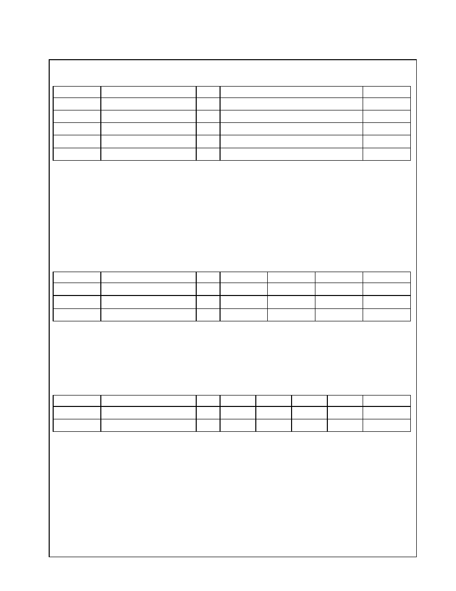
10. Pin Capacitance
(1)
(T
A
= 25∞C, f = 1MHz)
Note:
1. Sampled but not 100% tested.
Symbol
Parameter
Notes
Ratings
Unit
V
CC
Supply voltage
1,2
-0.2 to +4.6
V
V
IN
Input voltage
1,2,4
-0.2 to +3.9
V
T
A
Operating temperature
-25 to +85
∞C
T
STG
Storage temperature
-55 to +125
∞C
F-V
CCW
F-V
CCW
voltage
1,3,5
-0.3 to +13.0
V
Symbol
Parameter
Notes
Min.
Typ.
Max.
Unit
V
CC
Supply Voltage
3
2.7
3.0
3.3
V
V
IH
Input Voltage
V
CC
-0.4
(2)
V
CC
+0.2
(1)
V
V
IL
Input Voltage
-0.2
0.4
V
Symbol
Parameter
Notes
Min.
Typ.
Max.
Unit
Condition
C
IN
Input capacitance
15
pF
V
IN
= 0V
C
I/O
I/O capacitance
25
pF
V
I/O
= 0V
sharp

L R S 1 3 6 1 F
13
11. DC Electrical Characteristics
(6)
DC Electrical Characteristics
(T
A
= -25∞C to +85∞C, V
CC
= 2.7V to 3.3V )
Symbol
Parameter
Notes Min. Typ.
(1)
Max.
Unit
Conditions
I
LI
Input Leakage Current
± 1.5
µA
V
IN
= V
CC
or GND
I
LO
Output Leakage Current
± 1.5
µA
V
OUT
=V
CC
or GND
I
CCS
F-V
CC
Standby Current
4
4
20
µA
CMOS Input
F-CE = F-RP = F-V
CC
± 0.2V
I
CCAS
F-V
CC
Auto Power-Save Current
3,4
4
20
µA
CMOS Input
F-CE = GND ± 0.2V
I
CCD
F-V
CC
Reset Power-Down Current
4
4
20
µA
F-RP = GND ± 0.2V
I
OUT
(F-RY/BY) = 0mA
I
CCR
F-V
CC
Read Current
4
15
25
mA
CMOS Input
F-CE = GND, f = 5MHz, I
OUT
= 0mA
I
CCW
F-V
CC
Word Write or Set Lock-Bit
Current
2
5
17
mA F-V
CCW
= V
CCWH1
5
12
mA F-V
CCW
= V
CCWH2
I
CCE
F-V
CC
Block Erase, Full Chip Erase or
Clear Block Lock-Bits Current
2
4
17
mA F-V
CCW
= V
CCWH1
4
12
mA F-V
CCW
= V
CCWH2
I
CCWS
I
CCES
F-V
CC
Word Write or Block Erase
Suspend Current
1
6
mA F-CE = V
IH
I
CCWS
I
CCWR
F-V
CCW
Standby or Read Current
4
± 2
± 15
µA
F-V
CCW
F-V
CC
10
200
µA
F-V
CCW
> F-V
CC
I
CCWAS
F-V
CCW
Auto Power-Save Current
3,4
0.1
5
µA
CMOS Input
F-CE = GND ± 0.2V
I
CCWD
F-V
CCW
Reset Power-Down Current
4
0.1
5
µA
F-RP = GND ± 0.2V
I
CCWW
F-V
CCW
Word Write or Set Lock-Bit
Current
2
12
40
mA F-V
CCW
= V
CCWH1
30
mA F-V
CCW
= V
CCWH2
I
CCWE
F-V
CCW
Block Erase, Full Chip Erase
or Clear Block Lock-Bits Current
2
8
25
mA F-V
CCW
= V
CCWH1
20
mA F-V
CCW
= V
CCWH2
I
CCWWS
I
CCWES
F-V
CCW
Word Write or Block Erase
Suspend Current
10
200
µA
F-V
CCW
= V
CCWH1/2
I
SB
S-V
CC
Standby Current
1
15
µA
S-CE
1
, S-CE
2
S-V
CC
- 0.2V or
S-CE
2
0.2V
I
SB1
S-V
CC
Standby Current
3
mA S-CE
2
= V
IL
I
CC1
S-V
CC
Operation Current
45
mA
S-CE
1
= V
IL
,
S-CE
2
= V
IH
V
IN
= V
IL
or V
IH
t
CYCLE
= Min.
I
I/O
= 0mA
I
CC2
S-V
CC
Operation Current
8
mA
S-CE
1
= 0.2V,
S-CE
2
= S-V
CC
-0.2V,
V
IN
= S-V
CC
-0.2V
or 0.2V
t
CYCLE
= 1µs
I
I/O
= 0mA
sharp
L R S 1 3 6 1 F
14
DC Electrical Characteristics (Continue)
(T
A
= -25∞C to +85∞C, V
CC
= 2.7V to 3.3V )
Notes:
1. All currents are in RMS unless otherwise noted. Reference values at V
CC
= 3.0V and T
A
= +25∞C.
2. Sampled, not 100% tested.
3. The Automatic Power Savings (APS) feature is placed automatically power save mode that addresses not switching more
than 300ns while read mode.
4. CMOS inputs are either V
CC
± 0.2V or GND ± 0.2V. TTL inputs are either V
IL
or V
IH.
5. Block erases, full chip erase, word writes and lock-bits configurations are inhibited when F-V
CCW
V
CCWLK
and not
guaranteed in the range between V
CCWLK
(Max.) and V
CCWH
(Min.), and above V
CCWH
(Max.).
6. V
CC
includes both F-V
CC
and S-V
CC
.
7. Includes F-RY/BY.
8. Applying V
CCWH2
to F-V
CCW
during erase/write can only be done for a maximum of 1000 cycles on each block. F-V
CCW
may be connected to V
CCWH2
for a total of 80 hours maximum.
Symbol
Parameter
Notes
Min.
Typ.
(1)
Max.
Unit
Conditions
V
IL
Input Low Voltage
2
-0.2
0.4
V
V
IH
Input High Voltage
2
V
CC
-0.4
V
CC
+0.2
V
V
OL
Output Low Voltage
2,7
0.4
V
I
OL
= 0.5mA
V
OH
Output High Voltage
2,7
2
V
I
OH
= -0.5mA
V
CCWLK
F-V
CCW
Lockout during Normal
Operations
2,5
1
V
V
CCWH1
F-V
CCW
during Block Erase, Full Chip
Erase, Word Write or Lock-Bit
configuration Operations
2.7
3.3
V
V
CCWH2
F-V
CCW
during Block Erase, Full Chip
Erase, Word Write or Lock-Bit
configuration Operations
8
11.7
12.3
V
V
LKO
F-V
CC
Lockout Voltage
2
V
sharp
L R S 1 3 6 1 F
15
12. AC Electrical Characteristics for Flash Memory
12.1 AC Test Conditions
12.2 Read Cycle
(T
A
= -25∞C to +85∞C, F-V
CC
= 2.7V to 3.3V)
Note:
1. F-OE may be delayed up to t
ELQV
- t
GLQV
after the falling edge of F-CE without impact on t
ELQV
.
Input pulse level
0 V to 2.7 V
Input rise and fall time
10 ns
Input and Output timing Ref. level
1.35 V
Output load
1TTL + C
L
(50pF)
Symbol
Parameter
Notes
Min.
Max.
Unit
t
AVAV
Read Cycle Time
90
ns
t
AVQV
Address to Output Delay
90
ns
t
ELQV
F-CE to Output Delay
1
90
ns
t
PHQV
F-RP High to Output Delay
600
ns
t
GLQV
F-OE to Output Delay
1
40
ns
t
ELQX
F-CE to Output in Low-Z
0
ns
t
EHQZ
F-CE High to Output in High-Z
40
ns
t
GLQX
F-OE to Output in Low-Z
0
ns
t
GHQZ
F-OE High to Output in High-Z
15
ns
t
OH
Output Hold form Address, F-CE or F-OE Change, Whichever Occurs First
0
ns
sharp
L R S 1 3 6 1 F
16
12.3 Write Cycle (F-WE Controlled)
(1,5)
(T
A
= -25∞C to +85∞C, F-V
CC
= 2.7V to 3.3V)
Notes:
1. Read timing characteristics during block erase, full chip erase, word write and lock-bit configurations are the same as
during read-only operations. Refer to AC Characteristics for Read Cycle.
2. Sampled, not 100% tested.
3. Refer to Section 5. Command Definitions for Flash Memory for valid A
IN
and D
IN
for block erase, full chip erase, word
write or lock-bit configuration.
4. F-V
CCW
should be held at V
CCWH1/2
until determination of block erase, full chip erase, word write or lock-bit
configuration success (SR.1/3/4/5 = 0).
5. It is written when F-CE and F-WE are active. The address and data needed to execute a command are latched on the rising
edge of F-WE or F-CE (Whichever goes high first).
Symbol
Parameter
Notes
Min.
Max.
Unit
t
AVAV
Write Cycle Time
90
ns
t
PHWL
F-RP High Recovery to F-WE Going Low
2
1
µs
t
ELWL
F-CE Setup to F-WE Going Low
10
ns
t
WLWH
F-WE Pulse Width
50
ns
t
SHWH
F-WP V
IH
Setup to F-WE Going High
2
100
ns
t
VPWH
F-V
CCW
Setup to F-WE Going High
2
100
ns
t
AVWH
Address Setup to F-WE Going High
3
50
ns
t
DVWH
Data Setup to F-WE Going High
3
50
ns
t
WHDX
Data Hold from F-WE High
0
ns
t
WHAX
Address Hold from F-WE High
0
ns
t
WHEH
F-CE Hold from F-WE High
10
ns
t
WHWL
F-WE Pulse Width High
30
ns
t
WHRL
F-WE going High to F-RY/BY Going Low or SR.7 Going "0"
100
ns
t
WHGL
Write Recovery before Read
0
ns
t
QVVL
F-V
CCW
Hold from Valid SRD, F-RY/BY High-Z
2,4
0
ns
t
QVSL
F-WP V
IH
Hold from Valid SRD, F-RY/BY High-Z
2,4
0
ns
sharp
L R S 1 3 6 1 F
17
12.4 Write Cycle (F-CE Controlled)
(1,5)
(T
A
= -25∞C to +85∞C, F-V
CC
= 2.7V to 3.3V)
Notes:
1. In systems where F-CE defines the write pulse width (within a longer F-WE timing waveform), all setup, hold and inactive
F-WE times should be measured relative to the F-CE waveform.
2. Sampled, not 100% tested.
3. Refer to Section 5. Command Definitions for Flash Memory for valid A
IN
and D
IN
for block erase, full chip erase, word
write or lock-bit configuration.
4. F-V
CCW
should be held at V
CCWH1/2
until determination of block erase, full chip erase, word write or lock-bit
configuration success (SR.1/3/4/5=0).
5. It is written when F-CE and F-WE are active. The address and data needed to execute a command are latched on the rising
edge of F-WE or F-CE (Whichever goes high first).
Symbol
Parameter
Notes
Min.
Max.
Unit
t
AVAV
Write Cycle Time
90
ns
t
PHEL
F-RP High Recovery to F-CE Going Low
2
1
µs
t
WLEL
F-WE Setup to F-CE Going Low
0
ns
t
ELEH
F-CE Pulse Width
65
ns
t
SHEH
F-WP V
IH
Setup to F-CE Going High
2
100
ns
t
VPEH
F-V
CCW
Setup to F-CE Going High
2
100
ns
t
AVEH
Address Setup to F-CE Going High
3
50
ns
t
DVEH
Data Setup to F-CE Going High
3
50
ns
t
EHDX
Data Hold from F-CE High
0
ns
t
EHAX
Address Hold from F-CE High
0
ns
t
EHWH
F-WE Hold from F-CE High
0
ns
t
EHEL
F-CE Pulse Width High
25
ns
t
EHRL
F-CE going High to F-RY/BY Going Low or SR.7 Going "0"
100
ns
t
EHGL
Write Recovery before Read
0
ns
t
QVVL
F-V
CCW
Hold from Valid SRD, F-RY/BY High-Z
2,4
0
ns
t
QVSL
F- WP V
IH
Hold from Valid SRD, F-RY/BY High-Z
2,4
0
ns
sharp

L R S 1 3 6 1 F
18
12.5 Block Erase, Full Chip Erase, Word Write and Lock-Bits Configuration Performance
(3)
(T
A
= -25∞C to +85∞C, F-V
CC
= 2.7V to 3.3V)
Notes:
1. Reference values at T
A
= +25∞C and F-V
CC
= 3.0V, F-V
CCW
= 3.0V or 12.0V. Assumes corresponding lock-bits are not
set. Subject to change based on device characterization.
2. Excludes system-level overhead.
3. Sampled, not 100% tested.
4. A Latency time is required from issuing suspend command (F-WE or F-CE going high) until F-RY/BY going High-Z or
SR.7 going "1".
5. If the time between writing the Block Erase Resume command and writing the Block Erase Suspend command is shorter
than t
ERES
and both commands are written repeatedly, a longer time is required than standard block erase until the
completion of the operation.
Symbol
Parameter
Notes
F-V
CCW
= 2.7V to 3.3V
F-V
CCW
= 11.7V to 12.3V
Unit
Min.
Typ.
(1)
Max.
Min.
Typ.
(1)
Max.
t
WHQV1
t
EHQV1
Word Write Time
32K-Word Block
2
33
200
20
µs
4K-Word Block
2
36
200
27
µs
Block Write Time
32K-Word Block
2
1.1
4
0.66
s
4K-Word Block
2
0.15
0.5
0.12
s
t
WHQV2
t
EHQV2
Block Erase Time
32K-Word Block
2
1.2
6
0.9
s
4K-Word Block
2
0.6
5
0.5
s
Full Chip Erase Time
2
84
420
64
s
t
WHQV3
t
EHQV3
Set Lock-Bit Time
2
56
200
42
µs
t
WHQV4
t
EHQV4
Clear Block Lock-Bits Time
2
1
5
0.69
s
t
WHRZ1
t
EHRZ1
Word Write Suspend Latency Time to Read
4
6
15
6
15
µs
t
WHRZ2
t
EHRZ2
Erase Suspend Latency Time to Read
4
16
30
16
30
µs
t
ERES
Block Erase Resume command
- Block Erase Suspend command
5
600
600
µs
sharp

L R S 1 3 6 1 F
19
12.6 Flash Memory AC Characteristics Timing Chart
Read Cycle Timing Chart
V
IH
V
IL
Address(A)
V
IH
V
IL
F-CE(E)
V
IH
V
IL
F-OE(G)
V
IH
V
IL
F-WE(W)
V
OH
t
GLQX
t
ELQX
t
PHQV
t
AVQV
High - Z
t
ELQV
t
GLQV
t
AVAV
t
EHQZ
t
GHQZ
t
OH
High - Z
Address Stable
Data Valid
Valid Output
Standby
Device
Address Selection
V
OL
Data(D/Q)
F-V
CC
V
IH
V
IL
F-RP(P)
sharp

L R S 1 3 6 1 F
20
Write Cycle Timing Chart (F-WE Controlled)
High-Z
("1")
V
OL
("0")
F-RY/BY(R)
(SR. 7)
t
WHRL
V
IH
V
IL
Address(A)
V
IH
V
IL
F-CE(E)
V
IH
V
IL
F-OE(G)
V
IH
V
IL
F-WE(W)
V
OH
t
WHGL
t
WHWL
t
PHWL
t
VPWH
High - Z
D
IN
D
IN
D
IN
A
IN
1
2
3
4
5
6
A
IN
Data
Valid
SRD
t
WHDX
t
DVWH
t
WLWH
t
WHQV1,2,3,4
t
AVWH
t
AVAV
t
WHEH
t
ELWL
t
WHAX
t
QVSL
t
QVVL
t
SHWH
V
OL
Data(D/Q)
F-WP(S)
V
IH
V
IH
V
IL
V
CCWH1,2
V
CCWLK
V
IL
V
IL
F-RP(P)
F-V
CCW
(V)
Notes:
1. F-V
CC
power-up and standby.
2. Write each setup command.
3. Write each confirm command or valid address and data.
4. Automated erase or program delay.
5. Read status register data.
6. Write Read Array command.
sharp

L R S 1 3 6 1 F
21
Write Cycle Timing Chart (F-CE Controlled)
V
IH
V
IL
Address(A)
V
IH
V
IL
F-CE(E)
V
IH
V
IL
F-OE(G)
V
IH
V
IL
F-WE(W)
V
OH
t
EHGL
t
EHEL
t
PHEL
t
VPEH
High - Z
D
IN
D
IN
D
IN
A
IN
1
2
3
4
5
6
A
IN
Data
Valid
SRD
t
EHDX
t
DVEH
t
ELEH
t
EHQV1,2,3,4
t
AVEH
t
AVAV
t
EHWH
t
WLEL
t
EHAX
t
QVSL
t
QVVL
t
SHEH
V
OL
Data(D/Q)
F-WP(S)
V
IH
V
IH
V
IL
V
CCWH1,2
V
CCWLK
V
IL
V
IL
F-RP(P)
F-V
CCW
(V)
Notes:
1. F-V
CC
power-up and standby.
2. Write each setup command.
3. Write each confirm command or valid address and data.
4. Automated erase or program delay.
5. Read status register data.
6. Write Read Array command.
High-Z
("1")
V
OL
("0")
F-RY/BY(R)
(SR. 7)
t
EHRL
sharp

L R S 1 3 6 1 F
22
12.7 Reset Operations
(1,2)
(T
A
= -25∞C to +85∞C, F-V
CC
= 2.7V to 3.3V)
Notes:
1. If F-RP is asserted while a block erase, full chip erase, word write or lock-bit configuration operation is not executing, the
reset will complete within 100ns.
2. A reset time, t
PHQV
, is required from the later of F-RY/BY (SR.7) going High-Z ("1") or F-RP going high until outputs are
valid. Refer to AC Characteristics-Read Cycle for t
PHQV
.
3. When the device power-up, holding F-RP low minimum 100ns is required after F-V
CC
has been in predefined range and
also has been in stable there.
AC Waveform for Reset Operation
Symbol
Parameter
Notes
Min.
Max.
Unit
t
PLPH
F-RP Pulse Low Time
(If F-RP is tied to V
CC
, this specification is not applicable.)
100
ns
t
PLRZ
F-RP Low to Reset during Block Erase, Full Chip Erase, Word
Write or lock-bit configuration
30
µs
t
VPH
F-V
CC
= 2.7V to F-RP High
3
100
ns
V
IH
V
IL
F-RP(P)
V
IH
t
PLPH
(A) Reset During Read Array Mode
(B) Reset During Block Erase, Full Chip Erase,
Word Write or Lock-Bit configuration
(C) F-RP Rising Timing
t
PLRZ
t
VPH
V
IL
F-RP(P)
F-V
CC
V
IH
2.7V
V
IL
V
IL
F-RP(P)
t
PLPH
High - Z
("1")
V
OL
("0")
F-RY/BY(R)
(SR.7)
High - Z
("1")
V
OL
("0")
F-RY/BY(R)
(SR.7)
sharp
L R S 1 3 6 1 F
23
13. AC Electrical Characteristics for SRAM
13.1 AC Test Conditions
Note:
1. Including scope and socket capacitance.
13.2 Read Cycle
(T
A
= -25∞C to +85∞C, S-V
CC
= 2.7V to 3.3V)
Note:
1. Active output to High-Z and High-Z to output active tests specified for a ±200mV transition from steady state levels into
the test load.
Input pulse level
0.4V to 2.4V
Input rise and fall time
5 ns
Input and Output timing Ref. level
1.4V
Output load
1TTL + C
L
(30pF)
(1)
Symbol
Parameter
Notes
Min.
Max.
Unit
t
RC
Read Cycle Time
85
ns
t
AA
Address access time
85
ns
t
ACE1
Chip enable access time (S-CE
1
)
85
ns
t
ACE2
Chip enable access time (S-CE
2
)
85
ns
t
BE
Byte enable access time
85
ns
t
OE
Output enable to output valid
45
ns
t
OH
Output hold from address change
10
ns
t
LZ1
S-CE
1
Low to output active
1
10
ns
t
LZ2
S-CE
2
High to output active
1
10
ns
t
OLZ
S-OE Low to output active
1
5
ns
t
BLZ
S-UB or S-LB Low to output active
1
10
ns
t
HZ1
S-CE
1
High to output in High-Z
1
0
25
ns
t
HZ2
S-CE
2
Low to output in High-Z
1
0
25
ns
t
OHZ
S-OE High to output in High-Z
1
0
25
ns
t
BHZ
S-UB or S-LB High to output in High-Z
1
0
25
ns
sharp

L R S 1 3 6 1 F
24
13.3 Write Cycle
(T
A
= -25∞C to +85∞C, S-V
CC
= 2.7V to 3.3V)
Note:
1. Active output to High-Z and High-Z to output active tests specified for a ±200mV transition from steady state levels into
the test load.
Symbol
Parameter
Notes
Min.
Max.
Unit
t
WC
Write cycle time
85
ns
t
CW
Chip enable to end of write
70
ns
t
AW
Address valid to end of write
70
ns
t
BW
Byte select time
70
ns
t
AS
Address setup time
0
ns
t
WP
Write pulse width
60
ns
t
WR
Write recovery time
0
ns
t
DW
Input data setup time
35
ns
t
DH
Input data hold time
0
ns
t
OW
S-WE High to output active
1
5
ns
t
WZ
S-WE Low to output in High-Z
1
25
ns
sharp

L R S 1 3 6 1 F
25
13.4 SRAM AC Characteristics Timing Chart
Read Cycle Timing Chart
V
IH
V
IL
Address
V
IH
V
IL
S-CE
1
V
IH
V
IL
S-CE
2
V
IH
V
IL
S-UB
S-LB
V
IH
V
IL
S-OE
V
IH
V
IL
S-WE
V
OH
V
OL
DQ
OUT
t
AA
High - Z
High - Z
t
RC
t
HZ1,2
t
BHZ
t
OHZ
t
ACE1,2
t
LZ1,2
t
BLZ
t
OLZ
t
BE
t
OE
t
OH
Address Stable
Data Valid
Data Valid
Standby
Device
Address Selection
sharp

L R S 1 3 6 1 F
26
Write Cycle Timing Chart (S-WE Controlled)
V
IH
V
IL
Address
V
IH
V
IL
S-CE
1
V
IH
V
IL
S-CE
2
V
IH
V
IL
S-UB
S-LB
V
IH
V
IL
S-OE
V
IH
V
IL
S-WE
V
OH
t
WZ
t
OW
t
DH
t
DW
t
AW
High - Z
High - Z
t
WC
(5)
t
WR
(2)
t
CW
(3)
t
BW
(1)
t
WP
(4)
t
AS
Address Stable
Data Valid
Data Valid
Data Undefined
Standby
Device
Address Selection
V
OL
(7,8)
DQ
OUT
V
IH
V
IL
(6)
DQ
IN
Notes:
1. A write occurs during the overlap of a low S-CE
1
, a high S-CE
2
and a low S-WE.
A write begins at the latest transition among S-CE
1
going low, S-CE
2
going high and S-WE going low.
A write ends at the earliest transition among S-CE
1
going high, S-CE
2
going low and S-WE going high.
t
WP
is measured from the beginning of write to the end of write.
2. t
CW
is measured from the later of S-CE
1
going low or S-CE
2
going high to the end of write.
3. t
BW
is measured from the time of going low S-UB or low S-LB to the end of write.
4 . t
AS
is measured from the address valid to beginning of write.
5. t
WR
is measured from the end of write to the address change. t
WR
applies in case a write ends at S-CE
1
going high, S-CE
2
going low or S-WE going high.
6. During this period DQ pins are in the output state, therefore the input signals of opposite phase to the
outputs must not be applied.
7. If S-CE
1
goes low or S-CE
2
goes high simultaneously with S-WE going low or after S-WE going low,
the outputs remain in high impedance state.
8. If S-CE
1
goes high or S-CE
2
goes low simultaneously with S-WE going high or before S-WE going high,
the outputs remain in high impedance state.
sharp

L R S 1 3 6 1 F
27
Write Cycle Timing Chart (S-CE Controlled)
t
AW
(1)
t
WP
V
IH
V
IL
Address
V
IH
V
IL
S-CE
1
V
IH
V
IL
S-CE
2
V
IH
V
IL
S-UB
S-LB
V
IH
V
IL
S-OE
V
IH
V
IL
S-WE
V
OH
t
DH
t
DW
High - Z
t
WC
(5)
t
WR
(2)
t
CW
(3)
t
BW
(4)
t
AS
Address Stable
Data Valid
Data Valid
Standby
Device
Address Selection
V
OL
DQ
OUT
V
IH
V
IL
DQ
IN
Notes:
1. A write occurs during the overlap of a low S-CE
1
, a high S-CE
2
and a low S-WE.
A write begins at the latest transition among S-CE
1
going low, S-CE
2
going high and S-WE going low.
A write ends at the earliest transition among S-CE
1
going high, S-CE
2
going low and S-WE going high.
t
WP
is measured from the beginning of write to the end of write.
2. t
CW
is measured from the later of S-CE
1
going low or S-CE
2
going high to the end of write.
3. t
BW
is measured from the time of going low S-UB or low S-LB to the end of write.
4 . t
AS
is measured from the address valid to beginning of write.
5. t
WR
is measured from the end of write to the address change. t
WR
applies in case a write ends at S-CE
1
going high, S-CE
2
going low or S-WE going high.
sharp

L R S 1 3 6 1 F
28
Write Cycle Timing Chart (S-UB, S-LB Controlled)
V
IH
V
IL
Address
V
IH
V
IL
S-CE
1
V
IH
V
IL
S-CE
2
V
IH
V
IL
S-UB
S-LB
V
IH
V
IL
S-OE
V
IH
V
IL
S-WE
V
OH
t
DH
t
DW
t
AW
High - Z
t
WC
(5)
t
WR
(2)
t
CW
(3)
t
BW
(1)
t
WP
(4)
t
AS
Address Stable
Data Valid
Data Valid
Standby
Device
Address Selection
V
OL
DQ
OUT
V
IH
V
IL
DQ
IN
Notes:
1. A write occurs during the overlap of a low S-CE
1
, a high S-CE
2
and a low S-WE.
A write begins at the latest transition among S-CE
1
going low, S-CE
2
going high and S-WE going low.
A write ends at the earliest transition among S-CE
1
going high, S-CE
2
going low and S-WE going high.
t
WP
is measured from the beginning of write to the end of write.
2. t
CW
is measured from the later of S-CE
1
going low or S-CE
2
going high to the end of write.
3. t
BW
is measured from the time of going low S-UB or low S-LB to the end of write.
4 . t
AS
is measured from the address valid to beginning of write.
5. t
WR
is measured from the end of write to the address change. t
WR
applies in case a write ends at S-CE
1
going high, S-CE
2
going low or S-WE going high.
sharp

L R S 1 3 6 1 F
29
14. Data Retention Characteristics for SRAM
(T
A
= -25∞C to +85∞C)
Notes
1. Reference value at T
A
= 25∞C, S-V
CC
= 3.0V.
2. S-CE
1
S-V
CC
- 0.2V, S-CE
2
S-V
CC
- 0.2V (S-CE
1
controlled) or S-CE
2
0.2V (S-CE
2
controlled).
Data Retention timing chart (S-CE
1
Controlled)
(1)
Data Retention timing chart (S-CE
2
Controlled)
Symbol
Parameter
Note
Min.
Typ.
(1)
Max.
Unit
Conditions
V
CCDR
Data Retention Supply voltage
2
1.5
3.3
V
S-CE
2
0.2V or
S-CE
1
S-V
CC
- 0.2V
I
CCDR
Data Retention Supply current
2
1
15
µA
S-V
CC
= 3.0V
S-CE
2
0.2V or
S-CE
1
S-V
CC
- 0.2V
t
CDR
Chip enable setup time
0
ns
t
R
Chip enable hold time
t
RC
ns
S-V
CC
2.7V
Vcc-0.4V
V
CCDR
S-CE
1
0V
Data Retention mode
S-CE
1
S-V
CC
-0.2V
t
CDR
t
R
Note:
1. To control the data retention mode at S-CE
1
, fix the input level of
S-CE
2
between V
CCDR
and V
CCDR
-0.2V or 0V and 0.2V during the data retention mode.
S-V
CC
2.7V
S-CE
2
V
CCDR
0.4V
0V
Data Retention mode
S-CE
2
0.2V
t
CDR
t
R
sharp

L R S 1 3 6 1 F
30
15. Notes
This product is a stacked CSP package that a 32M (x16) bit Flash Memory and a 4M (x16) bit SRAM are assembled into.
- Supply Power
Maximum difference (between F-V
CC
and S-V
CC
) of the voltage is less than 0.3V.
- Power Supply and Chip Enable of Flash Memory and SRAM (F-CE, S-CE
1
, S-CE
2
)
S-CE
1
should not be "low" and S-CE
2
should not be "high" when F-CE is "low" simultaneously.
If the two memories are active together, possibly they may not operate normally by interference noises or data collision
on DQ bus.
Both F-V
CC
and S-V
CC
are needed to be applied by the recommended supply voltage at the same time expect SRAM
data retention mode.
- Power Up Sequence
When turning on Flash memory power supply, keep F-RP "low". After F-V
CC
reaches over 2.7V, keep F-RP "low" for
more than 100nsec.
- Device Decoupling
The power supply is needed to be designed carefully because one of the SRAM and the Flash Memory is in standby
mode when the other is active. A careful decoupling of power supplies is necessary between SRAM and Flash
Memory. Note peak current caused by transition of control signals (F-CE, S-CE
1
, S-CE
2
).
sharp
L R S 1 3 6 1 F
31
16. Flash Memory Data Protection
Noises having a level exceeding the limit specified in the specification may be generated under specific operating conditions on
some systems. Such noises, when induced onto F-WE signal or power supply, may be interpreted as false commands, causing
undesired memory updating. To protect the data stored in the flash memory against unwanted writing, systems operating with the
flash memory should have the following write protect designs, as appropriate.
The below describes data protection method.
1. Protecting data in specific block
∑ By setting a F-WP to low, only the boot block can be protected against overwriting. Parameter and main blocks cannot
be locked. System program, etc., can be locked by storing them in the boot block.
For further information on setting/resetting of lock bit, and controlling of F-WP and F-RP refer to the specification.
(See Chapter 5. Command Definitions for Flash Memory)
2. Data Protection through F-V
CCW
∑ When the level of F-V
CCW
is lower than V
CCWLK
(lockout voltage), write operation on the flash memory is disabled.
All blocks are locked and the data in the blocks are completely write protected.
∑ For the lockout voltage, refer to the specification. (See Chapter 11. DC Electrical Characteristics)
Data Protection during voltage transition
1. Data protection thorough F-RP
∑ When the F-RP is kept low during power up and power down sequence, write operation on the flash memory is
disabled, write protecting all blocks.
∑ For the details of F-RP control, refer to the specification.
(See Chapter 12. AC Electrical Characteristics for Flash Memory)
sharp

L R S 1 3 6 1 F
32
17. Design Considerations
1. Power Supply Decoupling
To avoid a bad effect to the system by flash memory power switching characteristics, each device should have a 0.1µ F
ceramic capacitor connected between its F-V
CC
and GND and between its F-V
CCW
and GND.
Low inductance capacitors should be placed as close as possible to package leads.
2. F-V
CCW
Trace on Printed Circuit Boards
Updating the memory contents of flash memories that reside in the target system requires that the printed circuit board
designer pay attention to the F-V
CCW
Power Supply trace. Use similar trace widths and layout considerations given to the
F-V
CC
power bus.
3. The Inhibition of Overwrite Operation
Please do not execute reprograming "0" for the bit which has already been programed "0". Overwrite operation may
generate unerasable bit.
In case of reprograming "0" to the data which has been programed "1".
∑ Program "0" for the bit in which you want to change data from "1" to "0".
∑ Program "1" for the bit which has already been programed "0".
For example, changing data from "1011110110111101" to "1010110110111100"
requires "1110111111111110" programing.
4. Power Supply
Block erase, full chip erase, word write and lock-bit configuration with an invalid F-V
CCW
(See Chapter 11. DC
Electrical Characteristics) produce spurious results and should not be attempted.
Device operations at invalid F-V
CC
voltage (See Chapter 11. DC Electrical Characteristics) produce spurious results
and should not be attempted.
18. Related Document Information
(1)
Note:
1. International customers should contact their local SHARP or distribution sales offices.
Document No.
Document Name
FUM99902
LH28F160BJ, LH28F320BJ Series Appendix
sharp

SPECIFICATIONS ARE SUBJECT TO CHANGE WITHOUT NOTICE.
Suggested applications (if any) are for standard use; See Important Restrictions for limitations on special applications. See Limited
Warranty for SHARP's product warranty. The Limited Warranty is in lieu, and exclusive of, all other warranties, express or implied.
ALL EXPRESS AND IMPLIED WARRANTIES, INCLUDING THE WARRANTIES OF MERCHANTABILITY, FITNESS FOR USE AND
FITNESS FOR A PARTICULAR PURPOSE, ARE SPECIFICALLY EXCLUDED. In no event will SHARP be liable, or in any way responsible,
for any incidental or consequential economic or property damage.
NORTH AMERICA
EUROPE
JAPAN
SHARP Microelectronics of the Americas
5700 NW Pacific Rim Blvd.
Camas, WA 98607, U.S.A.
Phone: (1) 360-834-2500
Fax: (1) 360-834-8903
Fast Info: (1) 800-833-9437
www.sharpsma.com
SHARP Microelectronics Europe
Division of Sharp Electronics (Europe) GmbH
Sonninstrasse 3
20097 Hamburg, Germany
Phone: (49) 40-2376-2286
Fax: (49) 40-2376-2232
www.sharpsme.com
SHARP Corporation
Electronic Components & Devices
22-22 Nagaike-cho, Abeno-Ku
Osaka 545-8522, Japan
Phone: (81) 6-6621-1221
Fax: (81) 6117-725300/6117-725301
www.sharp-world.com
TAIWAN
SINGAPORE
KOREA
SHARP Electronic Components
(Taiwan) Corporation
8F-A, No. 16, Sec. 4, Nanking E. Rd.
Taipei, Taiwan, Republic of China
Phone: (886) 2-2577-7341
Fax: (886) 2-2577-7326/2-2577-7328
SHARP Electronics (Singapore) PTE., Ltd.
438A, Alexandra Road, #05-01/02
Alexandra Technopark,
Singapore 119967
Phone: (65) 271-3566
Fax: (65) 271-3855
SHARP Electronic Components
(Korea) Corporation
RM 501 Geosung B/D, 541
Dohwa-dong, Mapo-ku
Seoul 121-701, Korea
Phone: (82) 2-711-5813 ~ 8
Fax: (82) 2-711-5819
CHINA
HONG KONG
SHARP Microelectronics of China
(Shanghai) Co., Ltd.
28 Xin Jin Qiao Road King Tower 16F
Pudong Shanghai, 201206 P.R. China
Phone: (86) 21-5854-7710/21-5834-6056
Fax: (86) 21-5854-4340/21-5834-6057
Head Office:
No. 360, Bashen Road,
Xin Development Bldg. 22
Waigaoqiao Free Trade Zone Shanghai
200131 P.R. China
Email: smc@china.global.sharp.co.jp
SHARP-ROXY (Hong Kong) Ltd.
3rd Business Division,
17/F, Admiralty Centre, Tower 1
18 Harcourt Road, Hong Kong
Phone: (852) 28229311
Fax: (852) 28660779
www.sharp.com.hk
Shenzhen Representative Office:
Room 13B1, Tower C,
Electronics Science & Technology Building
Shen Nan Zhong Road
Shenzhen, P.R. China
Phone: (86) 755-3273731
Fax: (86) 755-3273735