 | –≠–ª–µ–∫—Ç—Ä–æ–Ω–Ω—ã–π –∫–æ–º–ø–æ–Ω–µ–Ω—Ç: LRS1816 | –°–∫–∞—á–∞—Ç—å:  PDF PDF  ZIP ZIP |

Æ
Integrated Circuits Group
LRS1816
Stacked Chip
Two 64M (x16) Flash + One 32M (x16) Smartcombo RAM
(Model No.:
LRS1816)
Spec No.:
MFM2-J13913B
Issue Date:
November 1, 2001
P
RELIMINARY
P
RODUCT
S
PECIFICATIONS
LR S1816
∑ Handle this document carefully for it contains material protected by international copyright law.
Any reproduction, full or in part, of this material is prohibited without the express written permission
of the company.
∑ When using the products covered herein, please observe the conditions written herein and the
precautions outlined in the following paragraphs. In no event shall the company be liable for
any damages resulting from failure to strictly adhere to these conditions and precautions.
(1) The products covered herein are designed and manufactured for the following application areas.
When using the products covered herein for the equipment listed in Paragraph (2), even for the
following application areas, be sure to observe the precautions given in Paragraph (2). Never use
the products for the equipment listed in Paragraph (3).
∑ Office electronics
∑ Instrumentation and measuring equipment
∑ Machine tools
∑ Audiovisual equipment
∑ Home appliance
∑ Communication equipment other than for trunk lines
(2) Those contemplating using the products covered herein for the following equipment
which demands high reliability, should first contact a sales representative of the company and
then accept responsibility for incorporating into the design fail-safe operation, redundancy, and
other appropriate measures for ensuring reliability and safety of the equipment and the overall
system.
∑ Control and safety devices for airplanes, trains, automobiles, and other transportation
equipment
∑ Mainframe computers
∑ Traffic control systems
∑ Gas leak detectors and automatic cutoff devices
∑ Rescue and security equipment
∑ Other safety devices and safety equipment, etc.
(3) Do not use the products covered herein for the following equipment which demands extremely
high performance in terms of functionality, reliability, or accuracy.
∑ Aerospace equipment
∑ Communications equipment for trunk lines
∑ Control equipment for the nuclear power industry
∑ Medical equipment related to life support, etc.
(4) Please direct all queries and comments regarding the interpretation of the above three
Paragraphs to a sales representative of the company.
∑ Please direct all queries regarding the products covered herein to a sales representative of the
company.
sharp
LR S1816
1
Contents
1. Description. . . . . . . . . . . . . . . . . . . . . . . . . . . . . . . . . . . . . . . . . . . . . . . . . . . . . . . . . . . . . . . . . . . . . . . . . . . . . . . . . . . . . 2
2. Pin Configuration. . . . . . . . . . . . . . . . . . . . . . . . . . . . . . . . . . . . . . . . . . . . . . . . . . . . . . . . . . . . . . . . . . . . . . . . . . . . . . . . 3
3. Truth Table . . . . . . . . . . . . . . . . . . . . . . . . . . . . . . . . . . . . . . . . . . . . . . . . . . . . . . . . . . . . . . . . . . . . . . . . . . . . . . . . . . . . 5
3.1 Bus Operation. . . . . . . . . . . . . . . . . . . . . . . . . . . . . . . . . . . . . . . . . . . . . . . . . . . . . . . . . . . . . . . . . . . . . . . . . . . . . 5
3.2 Simultaneous Operation Modes Allowed with Four Planes . . . . . . . . . . . . . . . . . . . . . . . . . . . . . . . . . . . . . . . . . 6
4. Block Diagram. . . . . . . . . . . . . . . . . . . . . . . . . . . . . . . . . . . . . . . . . . . . . . . . . . . . . . . . . . . . . . . . . . . . . . . . . . . . . . . . . . 7
5. Command Definitions for Flash Memory . . . . . . . . . . . . . . . . . . . . . . . . . . . . . . . . . . . . . . . . . . . . . . . . . . . . . . . . . . . . . 8
5.1 Command Definitions . . . . . . . . . . . . . . . . . . . . . . . . . . . . . . . . . . . . . . . . . . . . . . . . . . . . . . . . . . . . . . . . . . . . . . 8
5.2 Identifier Codes for Read Operation . . . . . . . . . . . . . . . . . . . . . . . . . . . . . . . . . . . . . . . . . . . . . . . . . . . . . . . . . . 10
5.3 Functions of Block Lock and Block Lock-Down. . . . . . . . . . . . . . . . . . . . . . . . . . . . . . . . . . . . . . . . . . . . . . . . . 11
5.4 Block Locking State Transitions upon Command Write . . . . . . . . . . . . . . . . . . . . . . . . . . . . . . . . . . . . . . . . . . . 11
5.5 Block Locking State Transitions upon F-WP Transition . . . . . . . . . . . . . . . . . . . . . . . . . . . . . . . . . . . . . . . . . . . 12
6. Status Register Definition . . . . . . . . . . . . . . . . . . . . . . . . . . . . . . . . . . . . . . . . . . . . . . . . . . . . . . . . . . . . . . . . . . . . . . . . 13
7. Memory Map for Flash Memory . . . . . . . . . . . . . . . . . . . . . . . . . . . . . . . . . . . . . . . . . . . . . . . . . . . . . . . . . . . . . . . . . . . 16
7.1 Memory Map - F
1
Selected (F
1
-CE = "L", F
2
-CE = "H") . . . . . . . . . . . . . . . . . . . . . . . . . . . . . . . . . . . . . . . . . . 16
7.2 Memory Map - F
2
Selected (F
1
-CE = "H", F
2
-CE = "L") . . . . . . . . . . . . . . . . . . . . . . . . . . . . . . . . . . . . . . . . . . 17
8. Absolute Maximum Ratings . . . . . . . . . . . . . . . . . . . . . . . . . . . . . . . . . . . . . . . . . . . . . . . . . . . . . . . . . . . . . . . . . . . . . . 18
9. Recommended DC Operating Conditions . . . . . . . . . . . . . . . . . . . . . . . . . . . . . . . . . . . . . . . . . . . . . . . . . . . . . . . . . . . . 18
10. Pin Capacitance . . . . . . . . . . . . . . . . . . . . . . . . . . . . . . . . . . . . . . . . . . . . . . . . . . . . . . . . . . . . . . . . . . . . . . . . . . . . . . . 18
11. DC Electrical Characteristics . . . . . . . . . . . . . . . . . . . . . . . . . . . . . . . . . . . . . . . . . . . . . . . . . . . . . . . . . . . . . . . . . . . . . 19
12. AC Electrical Characteristics for Flash Memory . . . . . . . . . . . . . . . . . . . . . . . . . . . . . . . . . . . . . . . . . . . . . . . . . . . . . . 21
12.1 AC Test Conditions . . . . . . . . . . . . . . . . . . . . . . . . . . . . . . . . . . . . . . . . . . . . . . . . . . . . . . . . . . . . . . . . . . . . . . . 21
12.2 Read Cycle . . . . . . . . . . . . . . . . . . . . . . . . . . . . . . . . . . . . . . . . . . . . . . . . . . . . . . . . . . . . . . . . . . . . . . . . . . . . . . 21
12.3 Write Cycle (F-WE / F-CE Controlled) . . . . . . . . . . . . . . . . . . . . . . . . . . . . . . . . . . . . . . . . . . . . . . . . . . . . . . . . 22
12.4 Block Erase, Full Chip Erase, (Page Buffer) Program Performance . . . . . . . . . . . . . . . . . . . . . . . . . . . . . . . . . . 23
12.5 Flash Memory AC Characteristics Timing Chart . . . . . . . . . . . . . . . . . . . . . . . . . . . . . . . . . . . . . . . . . . . . . . . . 24
12.6 Reset Operations . . . . . . . . . . . . . . . . . . . . . . . . . . . . . . . . . . . . . . . . . . . . . . . . . . . . . . . . . . . . . . . . . . . . . . . . . 27
13. AC Electrical Characteristics for Smartcombo RAM . . . . . . . . . . . . . . . . . . . . . . . . . . . . . . . . . . . . . . . . . . . . . . . . . . 28
13.1 AC Test Conditions . . . . . . . . . . . . . . . . . . . . . . . . . . . . . . . . . . . . . . . . . . . . . . . . . . . . . . . . . . . . . . . . . . . . . . . 28
13.2 Read Cycle . . . . . . . . . . . . . . . . . . . . . . . . . . . . . . . . . . . . . . . . . . . . . . . . . . . . . . . . . . . . . . . . . . . . . . . . . . . . . . 28
13.3 Write Cycle . . . . . . . . . . . . . . . . . . . . . . . . . . . . . . . . . . . . . . . . . . . . . . . . . . . . . . . . . . . . . . . . . . . . . . . . . . . . . 29
13.4 Power Up Timing . . . . . . . . . . . . . . . . . . . . . . . . . . . . . . . . . . . . . . . . . . . . . . . . . . . . . . . . . . . . . . . . . . . . . . . . . 30
13.5 Sleep Mode Timing . . . . . . . . . . . . . . . . . . . . . . . . . . . . . . . . . . . . . . . . . . . . . . . . . . . . . . . . . . . . . . . . . . . . . . . 30
13.6 Address Skew Timing . . . . . . . . . . . . . . . . . . . . . . . . . . . . . . . . . . . . . . . . . . . . . . . . . . . . . . . . . . . . . . . . . . . . . 30
13.7 Data Retention Timing . . . . . . . . . . . . . . . . . . . . . . . . . . . . . . . . . . . . . . . . . . . . . . . . . . . . . . . . . . . . . . . . . . . . . 30
13.8 Smartcombo RAM AC Characteristics Timing Chart . . . . . . . . . . . . . . . . . . . . . . . . . . . . . . . . . . . . . . . . . . . . . 31
14. Notes . . . . . . . . . . . . . . . . . . . . . . . . . . . . . . . . . . . . . . . . . . . . . . . . . . . . . . . . . . . . . . . . . . . . . . . . . . . . . . . . . . . . . . . 38
15. Flash Memory Data Protection . . . . . . . . . . . . . . . . . . . . . . . . . . . . . . . . . . . . . . . . . . . . . . . . . . . . . . . . . . . . . . . . . . . 39
16. Design Considerations . . . . . . . . . . . . . . . . . . . . . . . . . . . . . . . . . . . . . . . . . . . . . . . . . . . . . . . . . . . . . . . . . . . . . . . . . . 40
17. Related Document Information . . . . . . . . . . . . . . . . . . . . . . . . . . . . . . . . . . . . . . . . . . . . . . . . . . . . . . . . . . . . . . . . . . . 40
sharp
LR S1816
2
1. Description
The LRS1816 is a combination memory organized as 4,194,304 x16 bit flash memory, 4,194,304 x16 bit flash memory and
2,097,152 x16 bit Smartcombo RAM in one package.
Features
- Power supply
∑ ∑ ∑ ∑
2.7V to 3.3V(Flash)
∑ ∑ ∑ ∑
2.7V to 3.1V(Smartcombo RAM)
- Operating temperature
∑ ∑ ∑ ∑
-25∞C to +85∞C
- Not designed or rated as radiation hardened
- 72pin CSP (LCSP072-P-0811) plastic package
- Flash memory has P-type bulk silicon, and Smartcombo RAM has P-type bulk silicon
Flash Memory
- F
1
: 64M (x16) bit Flash Memory, F
2
: 64M (x16) bit Flash Memory
- Access Time
∑ ∑ ∑ ∑
85 ns
(Max.)
- Power supply current for each Chip (The current for F-V
CC
pin and F-V
PP
pin)
Read
∑ ∑ ∑ ∑
26 mA
(Max. t
CYCLE
= 200ns, CMOS Input)
Word write
∑ ∑ ∑ ∑
61 mA
(Max.)
Block erase
∑ ∑ ∑ ∑
31 mA
(Max.)
Reset Power-Down
∑ ∑ ∑ ∑
50 µA
(Max. F-RST = GND ± 0.2V,
I
OUT
(F-RY/BY) = 0mA)
Standby
∑ ∑ ∑ ∑
50 µA
(Max. F-CE = F-RST = F-V
CC
± 0.2V)
- Optimized Array Blocking Architecture for each Chip
Eight 4K-word Parameter Blocks
One-hundred and twenty-seven 32K-word Main Blocks
F
1
: Top Parameter Location, F
2
: Bottom Parameter Location
- Extended Cycling Capability
100,000 Block Erase Cycles
(F-V
PP
= 1.65V to 3.3V)
1,000 Block Erase Cycles and total 80 hours
(F-V
PP
= 11.7V to 12.3V)
- Enhanced Automated Suspend Options
Word Write Suspend to Read
Block Erase Suspend to Word Write
Block Erase Suspend to Read
* In the following pages, F
1
, F
2
and F are defined as F
1
: 64M (x16) bit Flash, F
2
: 64M (x16) bit Flash, F: both Flashes in common.
Smartcombo RAM
- Access Time
∑ ∑ ∑ ∑
85 ns
(Max.)
- Cycle time
∑ ∑ ∑ ∑
85 to 32,000 ns
- Power Supply current
Operating current
∑ ∑ ∑ ∑
30 mA
(Max. t
RC
, t
WC
= Min.)
Standby current (Data retention current)
∑ ∑ ∑ ∑
100 µA
(Max.)
Sleep Mode (Data non-retention current)
∑ ∑ ∑ ∑
15 µA
(Max.)
sharp
LR S1816
3
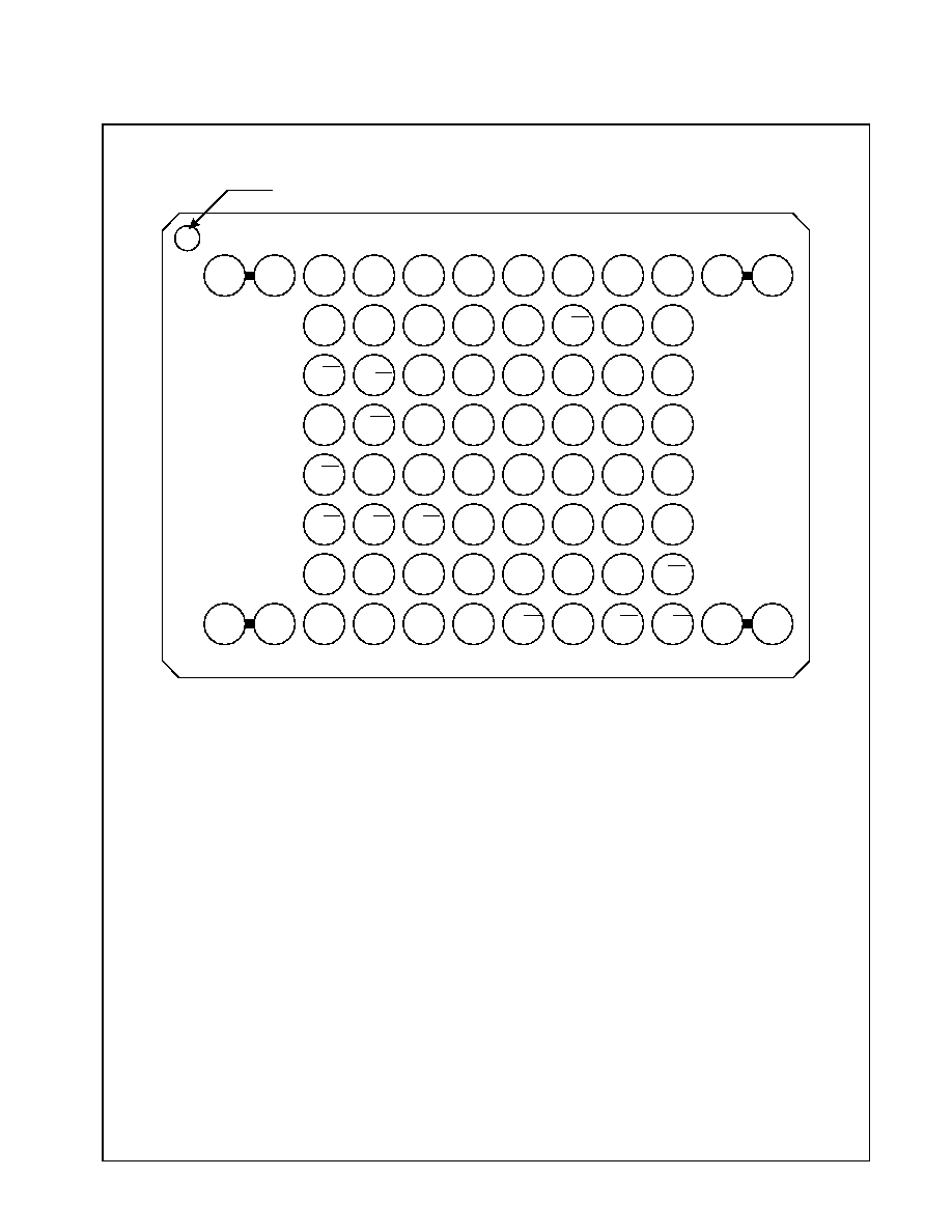
2. Pin Configuration
NC
NC
GND
A
16
A
11
A
8
A
10
A
15
A
14
A
9
DQ
15
A
13
A
12
1
2
3
4
5
6
7
8
S-WE
F-WE
F-RST
T
1
F-A
21
F-
RY/BY
S-A
17
T
2
DQ
12
DQ
13
DQ
6
S-CE
2
F-WP
S-LB
F-V
PP
S-UB S-OE
A
19
DQ
11
T
4
DQ
9
T
3
DQ
10
DQ
8
A
B
C
D
E
F
G
A
18
F-A
17
A
7
A
6
A
3
A
2
GND
9
DQ
14
DQ
4
S-V
CC
DQ
2
DQ
0
A
1
NC
10
DQ
7
DQ
5
F-V
CC
DQ
3
DQ
1
S-CE
1
NC
11
NC
12
NC
H
NC
NC
A
5
A
4
A
0
GND
F-OE F
2
-CE
NC
NC
F
1
-CE
INDEX
(TOP View)
A
20
Note) From T
1
to T
4
pins are needed to be open.
Two NC pins at the corner are connected.
Do not float any GND pins.
sharp