(Notice)
°
In the absence of confirmation by device specification sheets, SHARP takes no responsibility for any defects that may occur in equipment using any SHARP
devices shown in catalogs, data books, etc. Contact SHARP in order to obtain the latest device specification sheets before using any SHARP device.
(Internet)
°
Data for sharp's optoelectronic/power device is provided for internet.(Address http://www.sharp.co.jp/ecg/)
Parameter
Supply voltage for IC
Supply voltage for LED
Input voltage
Turn-on time
Operating temperature
Storage temperature
Power dissipation
Symbol
V
CC
V
LED
V
I
t
ON
T
opr
T
stg
P
Rating
-0.3 to +6.0
-0.3 to +5.5
-0.3 to V
CC
+0.3
1
-10 to +45
-25 to +85
35
Unit
V
V
V
ms
∞C
∞C
W
(Ta=25∞C)
Parameter
Supply voltage for IC
Supply voltage for LED
IC current dissipation
LED current dissipation
*1
Input voltage
Input current
Clock frequency
Frame frequency
Symbol
V
CC
V
LED
I
CC
I
LED
V
IH
V
IL
I
IH
I
IL
f
CLK
f
FR
MIN.
4.75
4.5
------
------
3.5
------
------
------
------
125
TYP.
5.0
5.0
270
5.0
------
------
------
------
------
200
MAX.
5.25
5.25
350
6.0
------
1.5
0.1
0.12
3.0
------
Unit
V
V
mA
A
V
V
µ
A
mA
MH
Z
H
Z
(V
CC
=5V,V
LED
=5V,Ta=25∞C)
*1 Under the condition that dichromatic all dots are lit.
tsu th
CLOCK
R&G
DATA
DATA out
R&G
t
WCLK
V
D
(n+2) data
V
D
(n+1) data
LATCH
Internal
ENABLE
R&G
ENABLE
ADDRESS
(A0 to A2)
tWL
tdD
td(E-L)
td(E-L)
td(A-E)
td(L-A)
td(C-L)
td(L-E)
1/f
OSC
ON
ON
ON
OFF
OFF
V
D
(n) data ON
V
D(
n)
V
D(
n+1)
V
D
(n+1) data ON
t
WENA
td(L-C)
167
s
Absolute Maximum Ratings
s
Electrical Characteristics
s
Timing Chart
s
Block Diagram
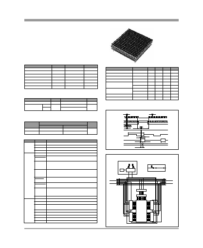
Dot Matrix LED Unit for Outdoor Use LT1447M(Lamp Type)
s
Features
°No. of dots : 16!16dots
°Outline dimensions : 144!144mm
°Dot size : ¯7.5mm
°Dot pitch : 9.0mm
°Radiation color : Yellow-green+Red(High-luminosity)dichromatic type
°Driving method : 1/8 duty dynamic drive
s
Optical Characteristics
s
Terminal Functions
Parameter
Viewing angle
Peak emission wavelength
Symbol2
2
1
/
2
p
TYP
40
660
565
Unit
∞
nm
(V
CC
=5V,V
LED
=5V,Ta=25
∞C
)
Red
Yellow-green
Each signal is used as input singal for next unit.
* As for the terminal number, refer to the outline dimensions.
Output signal
(CN3)
Input signal
(CN2)
Power supply
(CN1)
Connector
V
LED
Vcc
GND1
RDATA
LATCH
GENABLE
CLOCK
GND1
A0 to A2
RDATA
LATCH
GENABLE
CLOCK
GND1
GDATA
RENABLE
GDATA
Symbol
GND2
RENABLE
Serial data input for red(H=ON, L=OFF)
Shift from up to down in the unit
H
D16
/H
D31
/H
D0
/H
D15
Serial data input for yellow-green(H=ON, L=OFF)
Shift from up to down in the unit
H
D16
/H
D31
/H
D0
/H
D15
Latch signal of display data H: Serial data is converted
to parallel data. L: Contents are latched.
Controls ON/OFF of yellow-green LED
(H: LED OFF)
Clock signal for data transmission in the shift-
register.(L/H: serial data is shifted.)
Ground for signal (Connected to ground for IC)
Buffered input signal
Buffered input signal
Input signal generated through 32-bit shift
register
Buffered input signal
Input signal generated through 32-bit shift register
Buffered input signal
Buffered input signal
Ground for signal (Connected to ground for IC)
Function
Supply voltage for LED(+5V)
Supply voltage for IC(+5V)
Ground for IC
Ground for LED
Address specification signal for column driver
Controls ON/OFF of red LED
(H: LED OFF)
A0 to A2
SHIFT-REGISTER
16BIT
LATCH AND DRIVER
SHIFT-REGISTER
16BIT
LATCH AND DRIVER
SHIFT-REGISTER
16BIT
LATCH AND DRIVER
SHIFT-REGISTER
16BIT
LATCH AND DRIVER
HC367
331
473
Input/output circuit
Luminance adjustment circuit
HC123
VR2
VR1
MONO-MULTI
A0
A1
A2
CLOCK
GENABLE
LATCH
GDATA
RDATA
RENABLE
IN
OUT
PNP DRIVER
3 TO 8 DECODER
H
D0
H
D15
H
D0
H
D16
H
D31
H
D31
H
D16
V
D15
V
D0
MATRIX
16
!
16 DOT
LED
DICHROMATIC
OSC
A0
A1
A2
CLOCK
GENABLE
LATCH
GDATA
RDATA
RENABLE
LT1447M
s
Luminance
Radiation color
Red
Yellow-green
1
600
750
2
800
1 000
Unit
cd/m
2
(V
CC
=5V,V
LED
=5V,Ta=25∞C)
Rank
Luminance is classified into 2 ranks shown below.
(Notice)
°
In the absence of confirmation by device specification sheets, SHARP takes no responsibility for any defects that may occur in equipment using any SHARP
devices shown in catalogs, data books, etc. Contact SHARP in order to obtain the latest device specification sheets before using any SHARP device.
(Internet)
°
Data for sharp's optoelectronic/power device is provided for internet.(Address http://www.sharp.co.jp/ecg/)
178
159
P10
!
13=130
9.5
9.5
1
5
9
9
.
5
2
.
5
9
.
5
P
1
0
!
1
3
=
1
3
0
156
154
60
60
256-¯7.5
1
1
VR1
VR2
CN2
5
7
CN1
1
5
6
9
.
7
5
51
6
9
.
7
5
7
CN3
1
49
21
Depth7
1
5
.
8
4
7
0
6-M3
3
1
7 RDATA
CN2(Input signal)
4 GND
GENABLE
2
5 CLOCK
3 LATCH
1 GDATA
5 CLOCK
6 RENABLE
6 RENABLE
3 LATCH
1 GDATA
GENABLE
4 GND
2
7 RDATA
CN3(Output signal)
1 VLED
Pin connection
CN1(Power supply)
4 GND
5 VLED
3 VCC
2 GND
1
3
0
1
5
7
15
23
52
38
1.6t
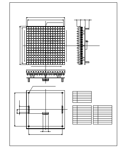
Dot Matrix LED Unit
Outline Dimensions(Unit:mm)
15
18
13.3
H
D16
H
D31
V
D15
P9.0
!
15=
P
9
.
0
!
1
5
=
D
a
t
a
s
h
i
f
t
d
i
r
e
c
t
i
o
n
135
144
256-¯7.5L E D
D0
H
1
3
5
1
4
4
4-M3(Depth 6MIN.)
Hexagonal spacer ASB315
V
D0
D15
H
LATCH
1
Ao
2
3
A1
A2
CN3(Output signal)
10
5
RDATA
6
GDATA
8
GENABLE
9
CLK
GND1
7
GND2
1
2
3
Ao
A1
A2
VDD
VLED
VLED
6
5
4
3
2
1
GND1
10
5
RDATA
6
GDATA
7
LATCH
8
9
CLK
GND1
GND2
6
1
19.8
10
125.58
1
10
4
RENABLE
2
2
.
5
1
2
5
.
5
8
1
5
CN1
4
CN3
CN2
RENABLE
GENABLE
CN2(Input signal)
CN1(Power supply)
1
Pin connection
11.6
12
HD16
HD15
HD13
HD47
HD63
VD15
VD0
159
HD32
148.5
(P9.9
!
15)
(
P
9
.
9
!
1
5
)
HD0
1
4
8
.
5
1
5
9
.
5
1 A0
CN2:Input signal
2 VLED
4 GND1
3 Vcc
1 VLED
CN1:Power supply
4 RENABLE
3 GND1
CN3:Output signal
1 A0
2 A1
10 GND1
9 CLK
7 LATCH
6 GDATA
5 RDATA
10 GND1
8 GENABLE
7 LATCH
6 GDATA
5 RDATA
9 CLK
3 GND1
6 GND2
5 GND2
2 A1
20
59.4
59.4
159
10
Height 3
132
10
VR2
VR1
1
CN2
CN1
6
CN3
1
1
0
6
4
7
1
5
9
1
6-M3(Depth10)
20
Water-proof ring
5
5
¯3 Boss
22
5
9
.
4
6
1
1
9
.
8
8 GENABLE
4 RENABLE
4
6
.
5
6
1
HD48
2
2
.
5
5
9
.
4
D
a
t
a
s
h
i
f
t
d
i
r
e
c
t
i
o
n
Pin connection
LT1448MA
LT1442M/LT1445M
LT1447M
9
10
11
RADJ
P14.9
!
15=223.5
239.2
P
1
4
.
9
!
1
5
=
2
2
3
.
5
1
2
0
.
0
HD16
HD31
HD0
HD15
1
1
9
.
6
VD0
VD15
11.0
MAX.
Height
(Except CN1 to 3)
8
0
.
0
2
0
6
.
0
11.0 18.0 16.6
206.0
190.0
217.0
CN1
6
177.0
60.0
1
5
0
.
0
5
0
.
0
10
1
CN3
10
2-
¯
3.0(Height3)
Positioning pin
Water-proof rubber
8-
¯
7.0 concave
2
1
7
.
0
1
1
9
.
6
1
1
9
.
6
1
5
9
.
0
P
2
.
5
!
9
=
2
2
.
5
P3.96
!
5=19.8
145.0
12-
(M3)
Insert nut
6
Depth
MIN.
45.0
1
0
.
0
9
.
0
1
GADJ
CN2
4
.
0
6.5
¯
7.0
¯
1
A0
2
3
4
5
6
7
8
9
10
A1
A2
RENABLE
RDATA
GDATA
LATCH
GENABLE
CLOCK
GND1
CN2
Pin No.
Name
Pin connection
(Input signal)
1
A0
2
3
4
5
6
7
8
9
10
A1
A2
RENABLE
RDATA
GDATA
LATCH
GENABLE
CLOCK
GND1
Pin No.
Name
(Output signal)
CN3
1
VLED
2
3
4
VLED
Vcc
GND1
CN1
Pin No.
Name
(Power supply)
5
GND2
6
GND2
2
5
.
0
2
5
.
0
256-13.0
!
13.0
D
a
t
a
s
h
i
f
t
d
i
r
e
c
t
i
o
n
LT1540M
12