In the absence of confirmation by device specification sheets, SHARP takes no responsibility for any defects that may occur in equipment using any SHARP devices
shown in catalogs, data books, etc. Contact SHARP in order to obtain the latest device spcification sheets before using any SHARP device.
LT262A
s
Operating Explanation
s
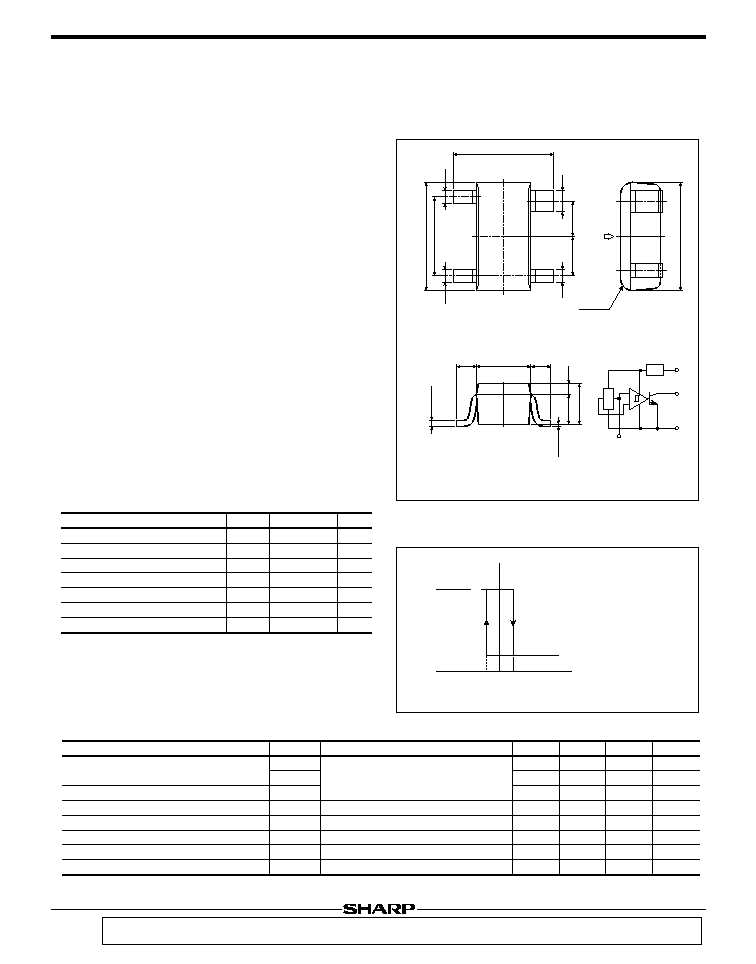
Outline Dimensions
(Unit : Fmm)
GaAs Hall IC for Noncontact Switch
(Alternating magnetic field-type*)
*Zero-cross is not warranted.
Hall IC
LT262A
s
Applications
°FDD
°HDD
°Water meter
°Car stereo
°Microswitch, etc.
s
Features
° Operation by small magnet due to high sensitivity
Operating point<10mT
°Combining a GaAs Hall device and an IC in a compact
package (2.9
X
1.5
X
1.1mm)
°Wide operation temperature range obtained by GaAs Hall
device (-20 to +125∞C)
°Long life time due to noncontact-type
*1 Soldering time : within 10 seconds
s
Absolute Maximum Ratings
(T
a
=25∞C)
Supply voltage
Output voltage
Output current
Power dissipation
Operating temperature
Storage temperature
Soldering temperature
*1
Symbol
V
CC
V
OUT
I
O
P
D
T
opr
T
stg
T
sol
Rating
8
8
5
100
-20 to +125
-55 to +150
260
Unit
V
V
mA
mW
∞C
∞C
∞C
Parameter
s
Electrical Characteristics
(T
a
=25∞C)
Operating magnetic flux density
Hysteresis breadth
Operating voltage
Supply current
Low level output voltage
Output leakage current
Operating point temperature drift
Symbol
B
OP
B
RP
B
H
V
CC
I
CC
V
OL
I
OH
B
OP
Condition
V
CC
=5V
V
OO
=5V
R
L
=10k
V
CC
=5V, B=<-10mT
I
O
=4mA, B>=10mT
V
CC
=5V, B=<-10mT, V
OO
=5V
V
CC
=5V, T
a
=-20∞C to +80∞C
MIN.
-
-10
-
3.5
-
-
-
-6
TYP.
-
-
-
-
-
-
-
-
MAX.
10
-
5
6.5
10.5
0.4
10
6
Unit
mT
mT
mT
V
mA
V
µ
A
mT
Parameter
+
-
H
REG
Terminal connections
Hall
device
2.7±0.3
1.5±0.2
1
2
4
3
0.6
0.4
0.4
0.4
1.9
2.9±0.2
0.85
0.95
2.9±0.2
4-R0.2
S
Z
0.6
0.6
0.3
0.8
(0to0.15)
0.16
+0.10
-0.06
1.1
+0.2
-0.1
1 : V
CC
2 : V
OUT
3 : Don't use.
4 : GND
Y
X
Hall device center line
X : +0.05±0.23mm against package center
Y : -0.05±0.1mm against package lead center between
No.2 and No.3 terminals
Z : 0.81±0.15mm from package surface
*No.3 terminal and the section of leads (both sides
of package in X direction) are connected with the
terminal of internal IC. Be careful in connecting other circuits.
B
RP
0 B
OP
+B
Magnetic flux density
<Alternating magnetic field-type>
Output voltage
As for dimensions of tape-packaged products, refer to page 44 .
Hall IC
LT262A
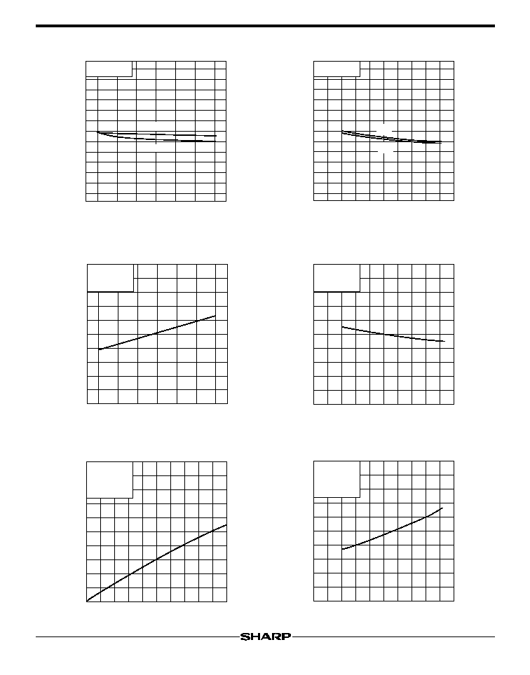
Fig. 1 Operating Magnetic Flux Density
vs. Supply Voltage
Fig. 3 Supply Current vs. Supply Voltage
Fig. 4 Supply Current vs. Ambient
Temperature
Fig. 5 Low Level Output Voltage vs.
Output Current
Fig. 6 Low Level Output Voltage vs.
Ambient Temperature
Fig. 2 Operating Magnetic Flux Density vs.
Ambient Temperature
T
a
=25∞C
B
OP
B
RP
-12
6.0
5.0
4.0
8
4
-4
-8
12
0
Operating magnetic flux density B
(mT)
Supply voltage V
CC
(V)
V
CC
=5V
B
OP
B
RP
-12
-40
120
40
80
0
8
4
-4
-8
12
0
Operating magnetic flux density B
(mT)
Ambient temperature T
a
(∞C)
V
CC
=5V
B=<-10mT
0
-40
120
0
40
80
10
8
6
4
2
Supply current I
CC
(mA)
Ambient temperature T
a
(∞C)
B=<-10mT
T
a
=25∞C
0
10
8
6
4
2
Supply current I
CC
(mA)
Supply voltage V
CC
(V)
6.0
5.0
4.0
V
CC
=5V
B>=10mT
T
a
=25∞C
0
0
4
1
2
3
5
0.5
0.4
0.3
0.2
0.1
Low level output voltage V
OL
(V)
Output current I
O
(mA)
V
CC
=5V
I
O
=4mA
B>=10mT
0
80
-40
0
40
120
0.5
0.4
0.3
0.2
0.1
Low level output voltage V
OL
(V)
Ambient temperature T
a
(∞C)