405 2
165 2
5
5
17.85 156.4
13.55 150.5
17.25 63.0
13.55 58.5
Positive
Negative
Positive
Negative
L
L
L
L
L
L
LT4070EA
LT4071EA
LT4082H
LT4082E
LT4083H
LT4083E
MIN.
4.75
4.75
4.75
4.75
4.75
4.75
TYP.
5.0
5.0
5.0
5.0
5.0
5.0
MAX.
5.25
5.25
5.25
5.25
5.25
5.25
TYP.
63
61
59
68
26
45
TYP.
565
565
585
565
585
565
30
30
30
30
30
30
TYP.
30
30
30
30
30
30
V
LED
(V)
5
5
5
5
5
5
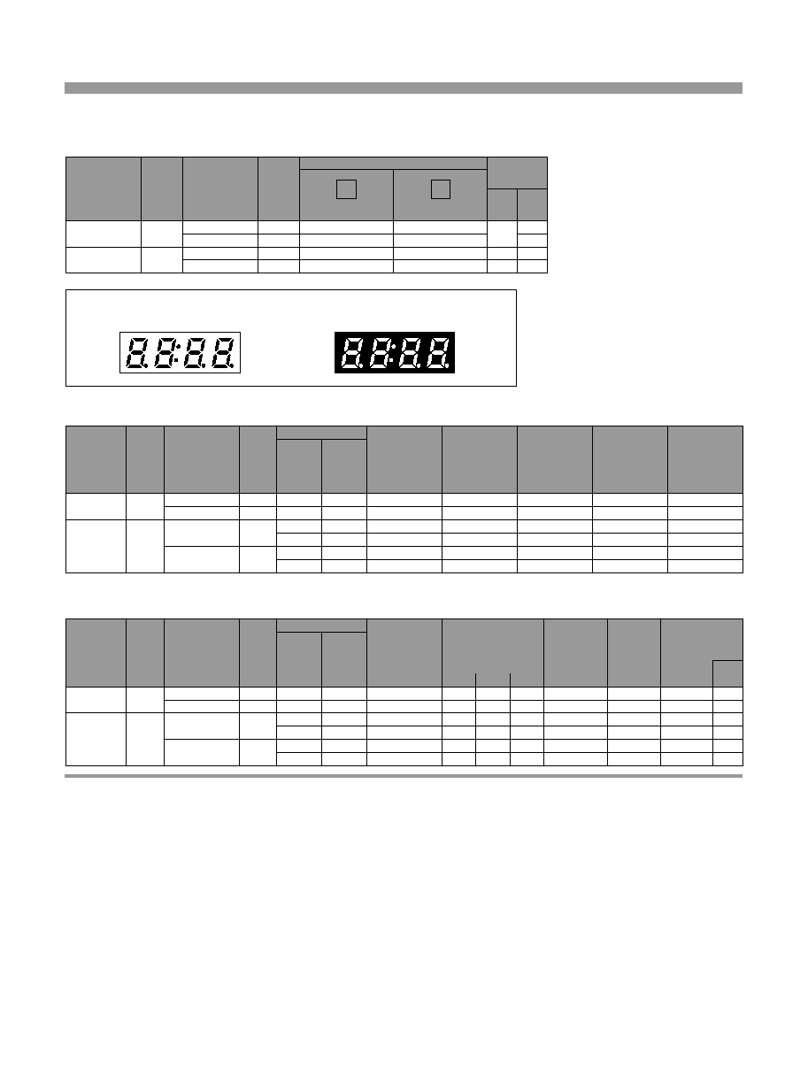
Display format
of LCD
LCD type
Supply
voltage
(V)
Radiation size(mm)
Radiation color
Yellow Yellow-green
Model No.
Operating voltage
V
LED
(V)
Luminous intensity
L
V
(cd/m
2
)
Peak emission
wavelength
l
p(nm)
Spectrum radiation bandwidth
D l(
nm)
(Ta=25∞C)
LED Panel Display
N
Absolute Maximum Ratings (Substrate Type)
N
Electro-optical Characteristics (Substrate Type)
405 2
165 2
5
5
17.85 156.4
13.55 150.5
17.25 63.0
13.55 58.5
Positive
Negative
Positive
Negative
L
L
L
L
L
L
LT4070EA
LT4071EA
LT4082H
LT4082E
LT4083H
LT4083E
20
20
20
20
20
20
5
5
5
5
5
5
-10 to +60
-10 to +60
-10 to +60
-10 to +60
-10 to +60
-10 to +60
-20 to +70
-20 to +70
-25 to +70
-25 to +70
-25 to +70
-25 to +70
Display format
of LCD
LCD type
Supply
voltage
(V)
Radiation
size(mm)
Radiation color
Yellow Yellow-green
Model No.
Forward current
*1
I
F
(mA)
Reverse voltage
V
R
(V)
Operating temperature
T
opr.
(∞C)
Storage temperature
T
stg.
(∞C)
*1 Per chip
(Ta=25∞C)
N
LED Panel Display(Substrate Type)
405 2
165 2
5
5
17.85 156.4
13.55 150.5
17.25 63.0
13.55 58.5
Positive
Negative
Positive
Negative
LT4082H
LT4083H
LT4070EA
LT4071EA
LT4082E
LT4083E
∆
∆
∆
14
15
12
13
Outline dimensions
Yellow
Display format of LCD
LCD type
Supply voltage
(V)
Radiation size
(mm)
Radiation color
Page
Figure
H
Yellow-green
E
Positive/Negative Display(White portion: Radiation color of backlight)
L
Positive
L
Negative
131
(Notice)
°
In the absence of confirmation by device specification sheets, SHARP takes no responsibility for any defects that may occur in equipment using any SHARP
devices shown in catalogs, data books, etc. Contact SHARP in order to obtain the latest device specification sheets before using any SHARP device.
(Internet)
°
Data for sharp's optoelectronic/power device is provided for internet.(Address http://www.sharp.co.jp/ecg/)
134
LED Panel Displays
Characteristics Diagrams
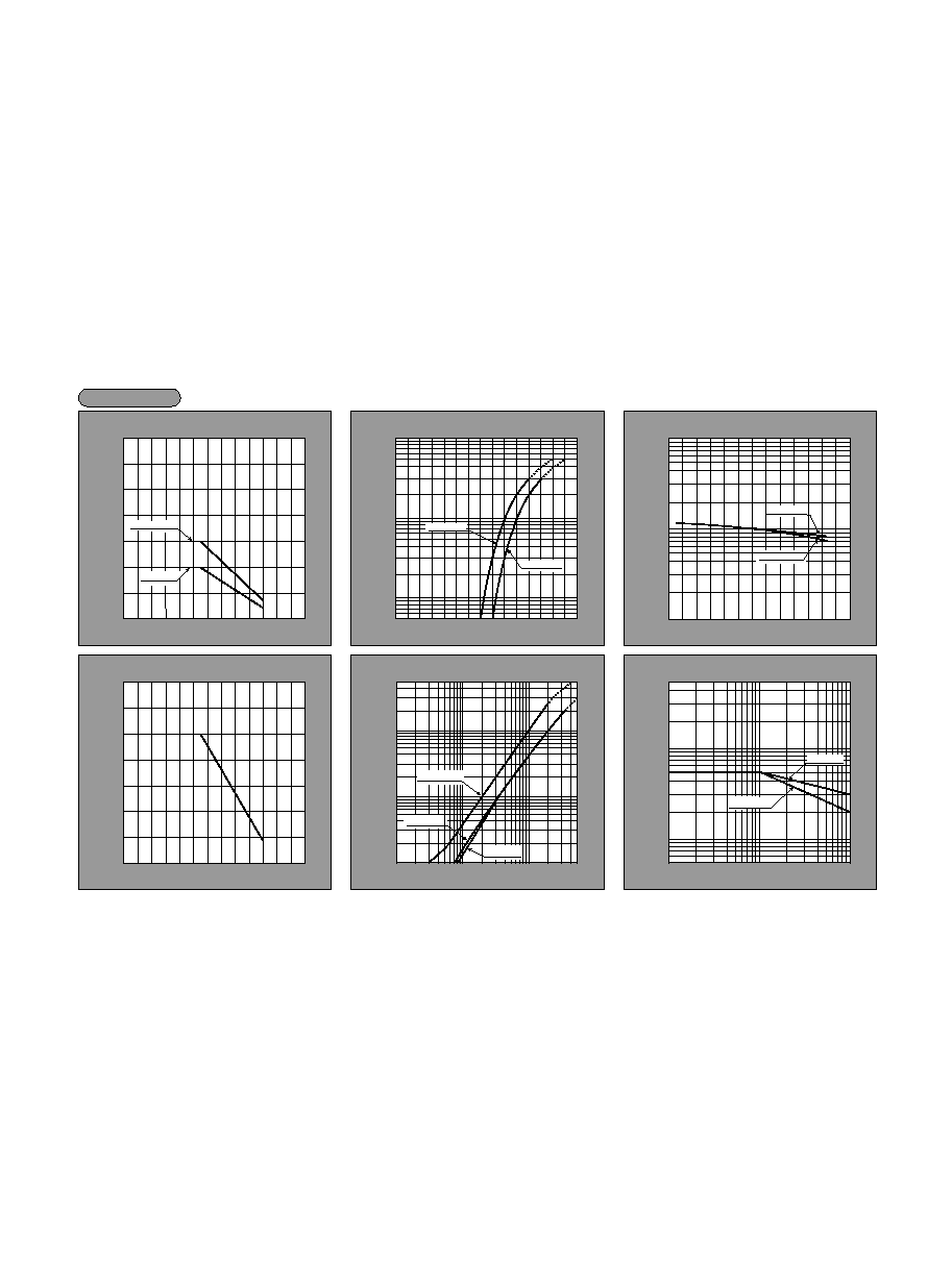
D series
H/E series
*
As for current conditions, refer to I
F
in electro-optical characteristics
*
1
H series I
F
=10mA
0
10
20
30
40
50
60
70
-20
0
20
40
60
100
80
0
10
20
30
40
50
60
70
-20
0
20
40
60
100
80
0.5
2
1
3
5
10
20
50
100
1.0
1.4
1.6
1.8
2.0
2.2
2.4
(T
a=
25
∞C)
1.2
1.1
1.3
1.5
1.7
1.9
2.1
2.3
2.5
1
2
5
200
100
20
50
10
500
0.1
0.2
0.5
1
2
5
10
20
50
(T
a=
25
∞C)
10
20
50
200
100
500
1000
-20
0
20
40
60
100
80
5
10
30
50
100
300
500
1/50
1/20
1/10
1/5
1/2
1
(T
a=
25
∞C)
H series
0
10
20
30
40
50
60
70
-20
0
20
40
60
100
80
0
10
20
30
40
50
60
70
-20
0
20
40
60
100
80
H series
E series
0.5
2
1
3
5
10
20
50
100
1.0
1.2
1.4
1.6
1.8
2.0
2.2
2.4
(T
a=
25
∞C
)
1.1
1.3
1.5
1.7
1.9
2.1
2.3
2.5
E series
1
2
5
200
100
20
50
10
500
0.1
0.2
0.5
1
2
5
10
20
50
(T
a=
25
∞C
)
H series
E series
H series
10
20
50
200
100
500
1000
-20
0
20
40
60
100
80
5
10
30
50
100
300
500
1/50
1/20
1/10
1/5
1/2
1
(T
a=
25
∞C
)
E series
H series
(*)
(*)
H series
*1
H/E series
Forward Current Derating Curve
Forward Current vs. Forward Voltage
Luminous Intensity vs. Ambient Temperature
Ambient temperature T
a(
∞C)
Forward voltage V
F
(V/chip)
Ambient temperature T
a(
∞C)
Forward current I
F
(mA/chip)
Forward current I
F
(mA/chip)
Relative luminous intensity(%)
Peak Forward Current Derating Curve
Luminous Intensity vs. Forward Current
Duty Ratio vs. Peak Forward Current
Peak forward current I
FM
(mA/chip)
Relative luminous intensity(%)
Peak forward current I
F
(mA/chip)
Ambient temperature T
a
(
∞C)
Forward current I
F
(mA/chip)
Duty ratio D
R
Forward Current Derating Curve
Forward Current vs. Forward Voltage
Luminous Intensity vs. Ambient Temperature
Forward current I
F
(mA/chip)
Forward current I
F
(mA/chip)
Relative luminous intensity(%)
Ambient temperature T
a
(
∞C)
Forward voltage V
F
(V/chip)
Ambient temperature T
a
(
∞C)
* As for current conditions, refer to I
F
in electro-optical characteristics
Peak Forward Current Derating Curve
Luminous Intensity vs. Forward Current
Duty Ratio vs. Peak Forward Current
Peak forward current I
FM
(mA/chip)
Relative luminous intensity(%)
Peak forward current I
F
(mA/chip)
Ambient temperature T
a
(
∞C)
Forward current I
F
(mA/dhip)
Duty ratio D
R
(Notice)
°
In the absence of confirmation by device specification sheets, SHARP takes no responsibility for any defects that may occur in equipment using any SHARP
devices shown in catalogs, data books, etc. Contact SHARP in order to obtain the latest device specification sheets before using any SHARP device.
(Internet)
°
Data for sharp's optoelectronic/power device is provided for internet.(Address http://www.sharp.co.jp/ecg/)
136
LED Panel Display
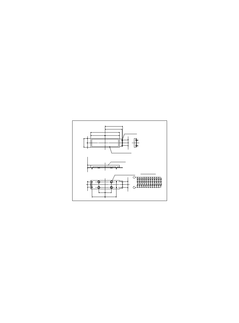
Outline Dimensions(Unit:mm)
1
2
5
6
3 4
Pin connection
Colored diffusion resin
1.5
0.5
6.4
6.4
8.0MAX
1.0
1
.
0
(
1
.
0
)
8
.
0
±
0
.
3
8
.
2
±
0
.
3
0
.
5
1
.
0
8
.
2
±
0
.
3
7
.
0
17.2
±
0.3
17.0
±
0.3
17.2
±
0.3
16.0
P
r
o
t
r
u
d
e
d
r
e
s
i
n
1
.
0
M
A
X
0.8MAX
2
.
4
N
O
M
2.4NOM
1
3
.
0
M
I
N
1
2
4
3
6
5
0
.
7
5
0
.
5
2
.
0
0.5
9
.
5
0
.
2
5
7
.
0
8
.
0
7.62NOM.
2.54NOM.
9.0
10.0
8
7
6
5
1
2
3
4
Colorless transparency resin
Pin connection
1
2
3
4
8
7
6
5
(
±
1
0
∞)
(
±
1
0
∞)
4
.
0
15.0
2.4
0.8
25.0
18.0
0.5
±
0.2
45.0
±
0.3
1.0
±
0.2
1.0
±
0.2
Radiation18
!
45
1.0
3.0
±
0.2
0.45
±
0.2
5.0
5.0
1
.
0
±
0
.
2
1
8
.
0
±
0
.
2
2
3
.
0
±
0
.
3
2
6
.
0
±
0
.
3
P
r
o
t
r
u
d
e
d
r
e
s
i
n
1
.
5
M
A
X
47.0
±
0.3
1
3
.
0
1
4
.
0
3
.
0
3
.
0
2
-
R
2
.
5
1
.
0
±
0
.
2
4
.
1
±
0
.
5
2
6
.
0
±
0
.
3
Pin connection
1
1 2
3 4
2
4
3
1
3
.
0
M
I
N
.
C-0.25
10
11 12
1
2
0.5
5
6
1
.
6
Radiation13.1
!
65.0
3.0
±
0.3
2
-
¯
1
.
5
3
.
0
1.0
1.0
4-R0.75
65.0
±
0.3
2
1
.
7
±
0
.
3
1
7
.
1
±
0
.
3
10.5
±
0.3
10.5
±
0.3
10.5
±
0.3
10.5
±
0.3
10.5
±
0.3
2.54NOM.
67.0
±
0.3
2
0
.
9
5
±
0
.
3
1
4
.
0
M
I
N
.
65.5
±
0.4
P
r
o
t
r
u
d
e
d
r
e
s
i
n
1
.
5
M
A
X
.
4
5
6
7
8
9
1
.
6
0.5
1
2
3
7
8
4
3
9
10
11
12
Pin connection
Radiation 13.5
!
102.0
1.5
2.5
4.0
±
0.3
105.0
±
0.4
1.5
102.0
±
0.4
1
2
.
0
M
I
N
2.4NOM.
2
-
¯
1
.
5
Pin connection
2.3
±
0.4
7
8
1
1
.
0
M
I
N
5
6
1
2
4
3
13
14
12
9
10
11
15
16
19
20
20
19
18
17
16
6-R0.75
0.45
2
2
.
5
±
0
.
3
2
.
1
±
0
.
5
1
.
0
6
5
4
0.5
3
2
1
12
103.5
±
0.4
10.0
±
0.3
10.0
±
0.3
10.0
±
0.3
10.0
±
0.3
10.0
±
0.3
10.0
±
0.3
10.0
±
0.3
10.0
±
0.3
10.0
±
0.3
2
4
.
6
±
0
.
8
1
7
.
0
11
10
100.0
±
0.4
2
.
0
0.8MAX
3
.
5
9
8
7
17
18
14
13
(
2
.
1
)
15
2-¯1.2hole
6
.
5
6
.
5
41.8
40.0
-0.3
-0.3
1
+0
+0
(34.0)
68.0
-
0
.
3
+
0
2
1
.
0
(
1
0
.
5
)
(
1
0
.
5
)
(34.0)
Radiation 63.0X17.2
2
Scattering seat
-
0
.
5
1
.
0
t
+
0
.
5
5
.
0
7
.
1
6
.
6
2
1
26.8
30.8
6
.
1
6
.
6
15.0 15.0
Calking 4-¯5MAX.
Pin connection
7
9
11
8
10
12
LT9230
u
Series
LT9400
u
Series,LT9400ED
LT9310
u
Series
LT9323
u
Series
LT9330
u
Series
LT4082
u
Series
(Notice)
°
In the absence of confirmation by device specification sheets, SHARP takes no responsibility for any defects that may occur in equipment using any SHARP
devices shown in catalogs, data books, etc. Contact SHARP in order to obtain the latest device specification sheets before using any SHARP device.
(Internet)
°
Data for sharp's optoelectronic/power device is provided for internet.(Address http://www.sharp.co.jp/ecg/)
137
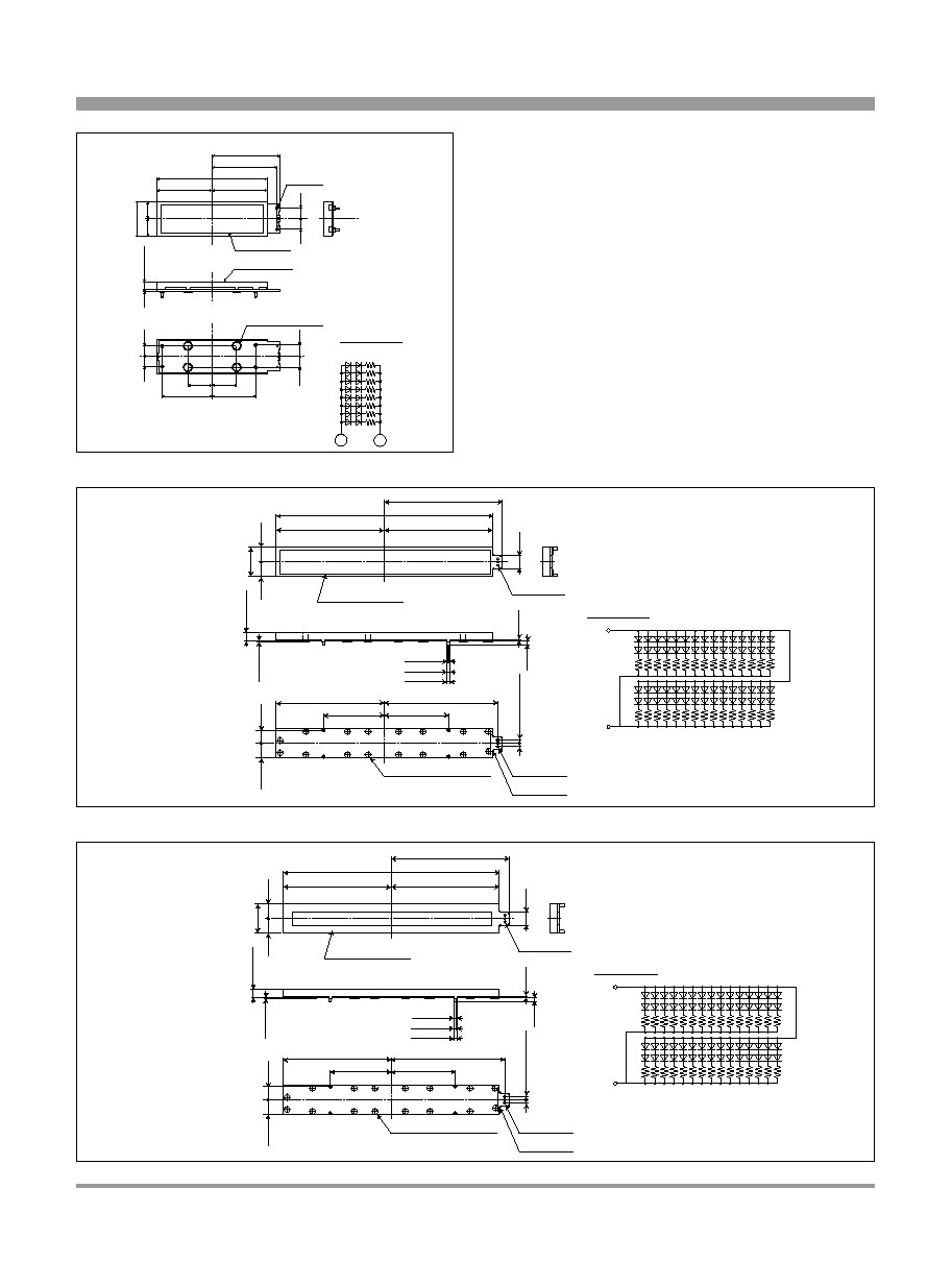
LED Panel Display
Outline Dimensions(Unit:mm)
7
.
1
A
6
.
6
6
.
6
15.0
26.8
B
A
6
.
1
30.8
15.0
Calking 4-¯5MAX
B
1
2
100
x 8 pcs.
5
.
0
±
0
.
5
1
.
0
t
Scattering seat
2
1
6
.
5
6
.
5
2-¯1.2hole
68.0
40.0
-0.3
+0
41.8
-0.3
+0
(
1
0
.
5
)
(
1
0
.
5
)
-
0
.
3
+
0
2
1
.
0
(34.0)
(34.0)
Emitting portion 58.5X13.5
Pin connection
1
Pin connection
3
.
3
3
2NC
1
2
3
87.3
80.0
1
.
0
4-¯1.0
159.6
79.6
2
2
.
0
1
1
.
0
7
.
0
M
A
X
.
84.0
47.5
16- ¯5.0MAX.(Calking)
P
2
.
5
4
!
2
=
5
.
0
8
4-¯2.5
1
1
.
0
1
0
.
0
44.5
1
0
.
0
79.1
Emitting portion17.8
!
156.4
2-R-0.5
2-R-0.5
1
0
.
0
3-¯1.0hole
4-¯1.5
0
.
5
M
A
X
(
C
a
l
k
i
n
g
)
1
Pin connection
3
.
3
3
2NC
1
2
3
87.3
80.0
1
.
0
4-¯1.0
159.6
79.6
2
2
.
0
1
1
.
0
7
.
0
M
A
X
.
84.0
47.5
16-¯5.0MAX.(Calking)
P
2
.
5
4
!
2
=
5
.
0
8
4-¯2.5
1
1
.
0
1
0
.
0
44.5
1
0
.
0
79.1
Emitting portion13.5
!
150.5
2-R-0.5
2-R-0.5
1
0
.
0
3-¯1.0hole
4-¯1.5
0
.
5
M
A
X
(
C
a
l
k
i
n
g
)
13
14
15
LT4083E LT4083H
LT4070EA
LT4071EA