 | –≠–ª–µ–∫—Ç—Ä–æ–Ω–Ω—ã–π –∫–æ–º–ø–æ–Ω–µ–Ω—Ç: LZ0P3610 | –°–∫–∞—á–∞—Ç—å:  PDF PDF  ZIP ZIP |
Document Outline
- ˛ˇ
- ˛ˇ
- ˛ˇ
- ˛ˇ
- ˛ˇ
- ˛ˇ
- ˛ˇ
- ˛ˇ
- ˛ˇ
- ˛ˇ
- ˛ˇ
- ˛ˇ
- ˛ˇ
- ˛ˇ
- ˛ˇ
- ˛ˇ
- ˛ˇ
- ˛ˇ
- ˛ˇ
- ˛ˇ
- ˛ˇ
In the absence of confirmation by device specification sheets, SHARP takes no responsibility for any defects that may occur in equipment using any SHARP devices shown in
catalogs, data books, etc. Contact SHARP in order to obtain the latest device specification sheets before using any SHARP device.
1
DESCRIPTION
The LZ0P3610/11/12
/15
are 1/4-type (4.5 mm)
270 000-pixel built-in lens color CCD (charge-
coupled device) area sensors. With their small lens
and WLCC-type flat package, it is possible to make
ultra small color camera easily.
FEATURES
∑ Number of effective pixels : 512 (H) x 492 (V)
∑ Number of optical black pixels
≠ Horizontal : 2 front and 28 rear
∑ Pixel pitch : 7.2 µm (H) x 5.6 µm (V)
∑ Mg, G, Cy, and Ye complementary color filters
∑ Low fixed-pattern noise and lag
∑ Blooming suppression structure
∑ Built-in output amplifier
∑ Built-in overflow drain voltage circuit and reset
gate voltage circuit
∑ Horizontal shift register clock and reset gate clock
voltage : 3.3 V (TYP.)
∑ Variable electronic shutter (1/60 to 1/10 000 s)
∑ Compatible with NTSC standard
∑ Built-in optical low-pass-filter
∑ Integrated lens :
Horizontal viewing angle
LZ0P3610 : 52∞
LZ0P3611 : 50∞
LZ0P3612 : 62∞
LZ0P3615 : 115∞
∑ Package
≠ 14-pin half-pitch WLCC
*
type
≠ Base section size : 12 mm (H) x 11 mm (V)
≠ Outline dimensions (MAX.) : 18 mm (H) x 11 mm (V)
∑ Package height
≠ Approx. 10 mm (single lens) : LZ0P3610
≠ Approx. 13 mm (two pcs. of lenses) :
LZ0P3611/12
/15
* Window Leadless Chip Carrier
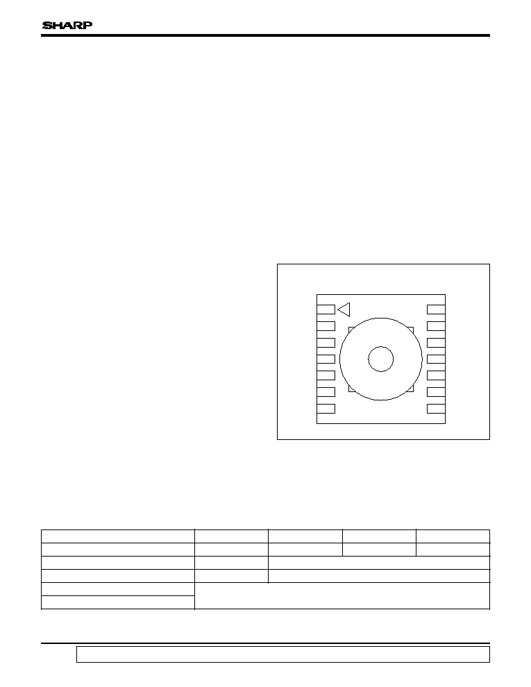
PIN CONNECTIONS
LZ0P3610/3611/3612/3615
LZ0P3610/3611/
3612
/3615
1/4-type Built-in Lens Color CCD
Area Sensors with 270 k Pixels
Under development
OD
ÿ
RS
NC
1
OS
NC
2
ÿ
H2
ÿ
H1
1
2
3
4
5
6
7
14
13
12
11
10
9
8
GND
ÿ
V4
ÿ
V3
ÿ
V2
ÿ
V1
PW
OFD
14-PIN HALF-PITCH WLCC TYPE
TOP VIEW
LZ0P3610
Horizontal viewing angle
Lens specification
Characteristics
Package height
Number of integrated lenses
LZ0P3615
LZ0P3612
LZ0P3611
52∞
115∞
62∞
50∞
Approx. 10 mm
Single
Two pcs.
Approx. 13 mm
Refer to each following specification.
COMPARISON TABLE
2
LZ0P3610/3611/3612/3615
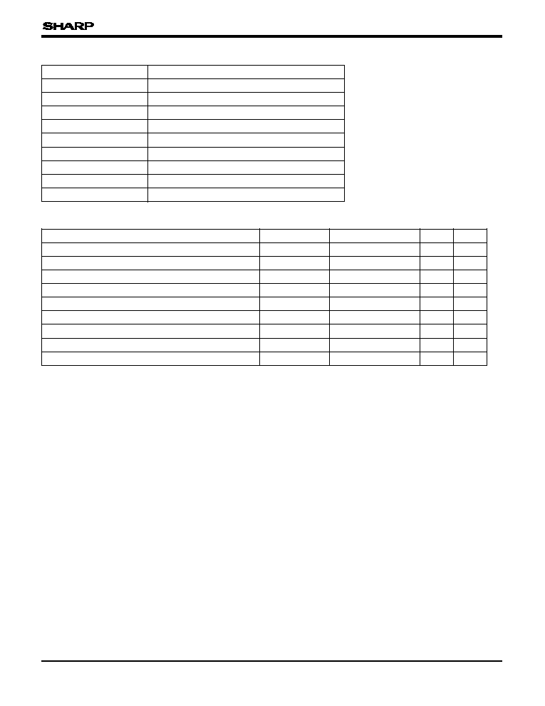
PIN DESCRIPTION
ABSOLUTE MAXIMUM RATINGS
(T
A
= +25 ∞C)
SYMBOL
PIN NAME
OD
Output transistor drain
OS
Output signals
ÿ
RS
Reset transistor clock
ÿ
V1
, ÿ
V2
, ÿ
V3
, ÿ
V4
Vertical shift register clock
ÿ
H1
, ÿ
H2
Horizontal shift register clock
OFD
Overflow drain
PW
P-well
GND
Ground
NC
1
, NC
2
No connection
PARAMETER
SYMBOL
RATING
UNIT
Output transistor drain voltage
V
OD
0 to +18
V
Overflow drain voltage
V
OFD
Internal output
V
Reset gate clock voltage
V
ÿRS
Internal output
V
Vertical shift register clock voltage
V
ÿV
≠10.5 to +17.5
V
Horizontal shift register clock voltage
V
ÿH
≠0.3 to +12
V
Voltage difference between P-well and vertical clock
V
PW
-V
ÿV
≠28 to 0
V
Voltage difference between vertical clocks
V
ÿV
-V
ÿV
0 to +15
V
≠20 to +70
∞C
Storage temperature
T
STG
≠10 to +60
∞C
Ambient operating temperature
T
OPR
3
2
1
NOTE
NOTES :
1. Do not connect to DC voltage directly. When OFD is connected to GND, connect V
OD
to GND. Overflow drain clock is
applied below 26 Vp-p.
2. Do not connect to DC voltage directly. When ÿ
RS
is connected to GND, connect V
OD
to GND. Reset gate clock is
applied below 8 Vp-p.
3. When clock width is below 10 µs, and clock duty factor is below 0.1%, voltage difference between vertical clocks will be
below 27 V.
3
LZ0P3610/3611/3612/3615
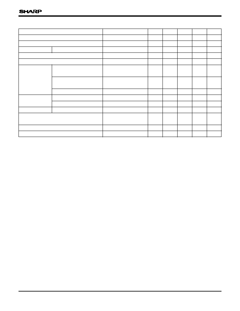
RECOMMENDED OPERATING CONDITIONS
PARAMETER
SYMBOL
MIN.
TYP.
MAX.
UNIT
NOTE
Ambient operating temperature
T
OPR
25.0
∞C
Output transistor drain voltage
V
OD
14.55
15.0
15.45
V
Overflow drain clock p-p level
23.5
V
1
V
ÿOFD
21.5
Ground
GND
0.0
V
P-well voltage
V
PW
≠9.0
V
ÿVL
V
2
Vertical shift
register clock
LOW level
V
ÿV1L
, V
ÿV2L
V
ÿV3L
, V
ÿV4L
≠8.5
≠8.0
≠7.5
V
INTERMEDIATE level
V
ÿV1I
, V
ÿV2I
V
ÿV3I
, V
ÿV4I
0.0
V
HIGH level
V
ÿV1H
, V
ÿV3H
14.55
15.0
15.45
V
Horizontal shift
register clock
LOW level
V
ÿH1L
, V
ÿH2L
≠0.05
0.0
0.05
V
HIGH level
V
ÿH1H
, V
ÿH2H
3.0
3.3
5.25
V
Reset gate clock p-p level
V
ÿRS
V
1
Vertical shift register clock frequency
f
ÿV1
, f
ÿV2
f
ÿV3
, f
ÿV4
15.73
kHz
Horizontal shift register clock frequency
f
ÿH1
, f
ÿH2
9.53
MHz
Reset gate clock frequency
f
ÿRS
9.53
MHz
NOTES :
∑ Connect NC
1
and NC
2
to GND directly or through a capacitor larger than 0.047 µF.
1. Use the circuit parameter indicated in "SYSTEM CONFIGURATION EXAMPLE", and do not connect to DC voltage directly.
2. V
PW
is set below V
ÿVL
that is low level of vertical shift register clock, or is used with the same power supply that is connected
to V
L
of V driver IC.
* To apply power, first connect GND and then turn on V
OD
. After turning on V
OD
, turn on PW first and then turn on other powers
and pulses. Do not connect the device to or disconnect it from the plug socket while power is being applied.
3.0
3.3
5.25
4
LZ0P3610/3611/3612/3615
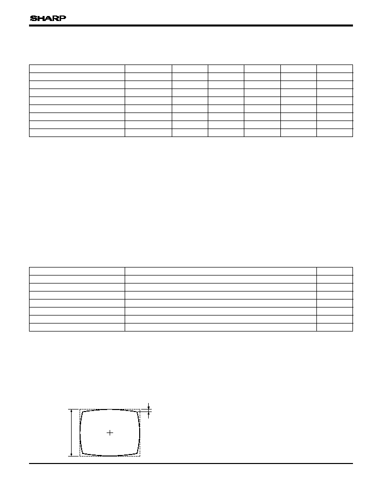
CHARACTERISTICS FOR LZ0P3610
(Drive method : Field accumulation)
(T
A
: +25 ∞C, Operating conditions : The typical values specified in "RECOMMENDED OPERATING CONDITIONS".
Color temperature of light source : 3 200 K)
LENS SPECIFICATION FOR LZ0P3610
NOTES :
1. The average output voltage in the central area (H/10,
V/10) under uniform illumination.
The standard exposure conditions are defined as when
V
O
is 150 mV.
2. The average output voltage in the central area (H/10,
V/10) under 10 times exposure of the standard exposure
conditions.
3. The average output voltage in the central area (H/10,
V/10) when a 1 000 lux light source with a white board
of 90% reflector is imaged.
4. The resolution in the central area (H/10, V/10) at which
the image of the TV resolution chart (ex. EIAJ test chart)
can be distinguished on the B/W video monitor.
5. The resolution in the peripheral area (image height : Y =
0.8) under the conditions mentioned above.
6. Defined by the following formula at the brightness of
standard output voltage : (Vco/Vce) x 100 [%]
Vco : Output voltage at edge of the image (at video output).
Vce : Output voltage at center of the image (at video output).
7. The difference between the center position of image and
that of the monitor. This is the ratio for the horizontal
underscanning monitor size which includes the decentering
eccentricity when turning the lens head one time.
PARAMETER
SYMBOL
Standard output voltage
V
O
Saturation output voltage
V
SAT
700
MIN.
TYP.
150
500
400
R
Sensitivity
3
2
1
NOTE
mV
mV
mV
UNIT
MAX.
8.0
mA
Output transistor drain current
I
OD
4.0
%
6
Shading
50
65
TV line
4
Resolution (at center)
250
300
PARAMETER
SPECIFICATION
Construction
Single (non-spherical, plastic)
Focal length
4.0 mm [TYP. : reference]
NOTE
2.8±5%
F No.
Focus adjustment range
to 10 cm
2
TV distortion
≠3.2%
1
Viewing angle
H : 52∞, V : 40∞, Diagonal : 65∞ [TYP. : reference]
NOTES :
1. TV distortion is defined by the formula, (y/y) x 100 [%]
at capturing rectangular pattern sized horizontal by
vertical as 4 by 3.
"y" is defined as the vertical height of the center of the
horizontal line.
y is defined as the difference between the vertical height
of the center of the horizontal line and an edge of it.
2. The best focus point of an object can be obtained by
turning the lens head within this range.
3. Torques which are necessary for turning the lens.
* Be careful not to remove the lens head by turning it
counterclockwise too much when adjusting macro.
y
y
200
150
Resolution (at corner)
5
TV line
Difference of center position
7
%
±10
3
0.00005 to 0.001 N∑m
Torque of focusing

5
LZ0P3610/3611/3612/3615
CHARACTERISTICS FOR LZ0P3611
(Drive method : Field accumulation)
(T
A
: +25 ∞C, Operating conditions : The typical values specified in "RECOMMENDED OPERATING CONDITIONS".
Color temperature of light source : 3 200 K)
LENS SPECIFICATION FOR LZ0P3611
NOTES :
1. The average output voltage in the central area (H/10,
V/10) under uniform illumination.
The standard exposure conditions are defined as when
V
O
is 150 mV.
2. The average output voltage in the central area (H/10,
V/10) under 10 times exposure of the standard exposure
conditions.
3. The average output voltage in the central area (H/10,
V/10) when a 1 000 lux light source with a white board
of 90% reflector is imaged.
4. The resolution in the central area (H/10, V/10) at which
the image of the TV resolution chart (ex. EIAJ test chart)
can be distinguished on the B/W video monitor.
5. The resolution in the peripheral area (image height : Y =
0.8) under the conditions mentioned above.
6. Defined by the following formula at the brightness of
standard output voltage : (Vco/Vce) x 100 [%]
Vco : Output voltage at edge of the image (at video output).
Vce : Output voltage at center of the image (at video output).
7. The difference between the center position of image and
that of the monitor. This is the ratio for the horizontal
underscanning monitor size which includes the decentering
eccentricity when turning the lens head one time.
PARAMETER
SYMBOL
Standard output voltage
V
O
Saturation output voltage
V
SAT
700
MIN.
TYP.
150
500
400
R
Sensitivity
3
2
1
NOTE
mV
mV
mV
UNIT
MAX.
8.0
mA
Output transistor drain current
I
OD
4.0
%
6
Shading
40
60
TV line
4
Resolution (at center)
250
300
PARAMETER
SPECIFICATION
Construction
2 pcs. (non-spherical, plastic)
Focal length
3.9 mm [TYP. : reference]
NOTE
2.8±5%
F No.
Focus adjustment range
to 10 cm
2
TV distortion
≠1.0%
1
Viewing angle
H : 50∞, V : 38∞, Diagonal : 60∞ [TYP. : reference]
NOTES :
1. TV distortion is defined by the formula, (y/y) x 100 [%]
at capturing rectangular pattern sized horizontal by
vertical as 4 by 3.
"y" is defined as the vertical height of the center of the
horizontal line.
y is defined as the difference between the vertical height
of the center of the horizontal line and an edge of it.
2. The best focus point of an object can be obtained by
turning the lens head within this range.
3. Torques which are necessary for turning the lens.
* Be careful not to remove the lens head by turning it
counterclockwise too much when adjusting macro.
y
y
200
150
Resolution (at corner)
5
TV line
Difference of center position
7
%
±10
3
0.00005 to 0.001 N∑m
Torque of focusing