PACKAGES FOR CCD AND CMOS DEVICES
11
,,,,,,,,,,,,,,,,,,,,,,,,,,,,,
,,,,,,,,,,,,,,,,,,,,,,,,,,,,,
,,,,,,,,,,,,,,,,,,,,,,,,,,,,,
,,,,,,,,,,,,,,,,,,,,,,,,,,,,,
,,,,,,,,,,,,,,,,,,,,,,,,,,,,,
,,,,,,,,,,,,,,,,,,,,,,,,,,,,,
,,,,,,,,,,,,,,,,,,,,,,,,,,,,,
,,,,,,,,,,,,,,,,,,,,,,,,,,,,,
,,,,,,,,,,,,,,,,,,,,,,,,,,,,,
,,,,,,,,,,,,,,,,,,,,,,,,,,,,,
,,,,,,,,,,,,,,,,,,,,,,,,,,,,,
,,,,,,,,,,,,,,,,,,,,,,,,,,,,,
,,,,,,,,,,,,,,,,,,,,,,,,,,,,,
,,,,,,,,,,,,,,,,,,,,,,,,,,,,,
,,,,,,,,,,,,,,,,,,,,,,,,,,,,,
,,,,,,,,,,,,,,,,,,,,,,,,,,,,,
,,,,,,,,,,,,,,,,,,,,,,,,,,,,,
,,,,,,,,,,,,,,,,,,,,,,,,,,,,,
,,,,,,,,,,,,,,,,,,,,,,,,,,,,,
,,,,,,,,,,,,,,,,,,,,,,,,,,,,,
,,,,,,,,,,,,,,,,,,,,,,,,,,,,,
,,,,,,,,,,,,,,,,,,,,,,,,,,,,,
,,,,,,,,,,,,,,,,,,,,,,,,,,,,,
,,,,,,,,,,,,,,,,,,,,,,,,,,,,,
,,,,,,,,,,,,,,,,,,,,,,,,,,,,,
,,,,,,,,,,,,,,,,,,,,,,,,,,,,,
,,,,,,,,,,,,,,,,,,,,,,,,,,,,,
,,,,,,,,,,,,,,,,,,,,,,,,,,,,,
,,,,,,,,,,,,,,,,,,,,,,,,,,,,,
,,,
,,,
,,,
,,,
,,,
,,,
,,,
,,,
,,,
,,,
,,,
,,,
,,,
,,,
,,,
,,,
,,,,,,,,
,,,,,,,,
,,,,,,,,
,,,,,,,,
,,,,,,,,
,,,,,,,,
,,,,
,,,,
,,,,
,,,,
,,,,
,,,
,,,
,,,
,,,
,,,
,,,
,,,
,,,
,,,
,,,
,,,
,,,
,,,
,,,
,,,
,,,
,,,
,,,
,,,
,,,
,,,
,,,
,,,
,,,
,,,
,,,
,,,
,,,
,,,
,,,
,,,
,,,
,,,
,,,
,,,
,,,
,,,
,,,
,,,
,,,
,,,
,,,
,,,
,,,
,,,
,,,
,,,
,,,
,,,
,,,
,,,
,,,
,,,
,,,
,,,
,,,
,,,
,,,
,,,
,,,
,,,
,,,
,,,
,,,
,,,
,,,
,,,
,,,
,,,
,,,
,,,
,,,
,,,
,,,
,,,
,,,
,,,
,,,
,,,
,,,
,,,
,,,
,,,
,,,
,,,
,,,
,,,
,,,
,,,
,,,
,,,
,,,
,,,
,,,
,,,
,,,
,,,
,,,
,,,
,,,
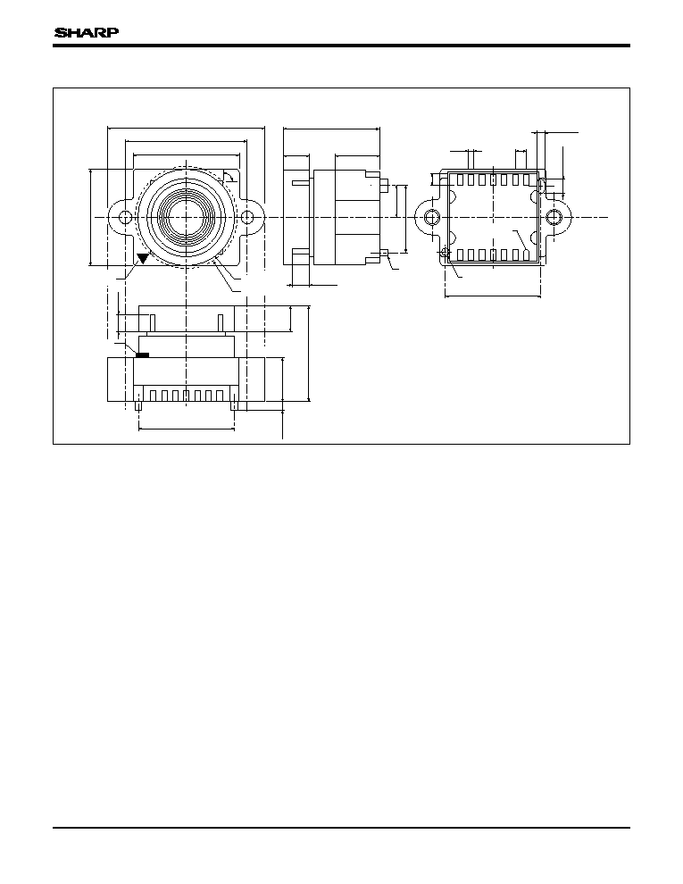
18
11
3.0
±0.1
5.0
±0.1
Approx.12-13
2-ÿ0.8
0.8
1.6
2-C0.2
14
±0.1
12
4-90∞
5.0
±0.1
Approx. 12
11.0
±0.05
Height 0.5
3.0
±0.1
1.0
±0.1
2.0
±0.1
11
±0.05
7.6
±0.05
3.6
1.27
0.64
1.27
2.0
±0.1
+0
≠0.2
+0
≠0.1
+0
≠0.05
+0
≠0.05
+0
≠0.05
+0 ≠0.1
+0 ≠0.05
No.1 index
ÿ11.0
ÿ12.0
+0
≠0.05
+0
≠0.05
No.1 index
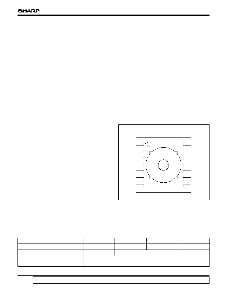
14 WLCC TYPE
øApplicable models°
LZ0P3611/12/15,
LZ0P3621/22/25,
LZ0P3641/42/45/46
PACKAGE
(Unit : mm)