 | –≠–ª–µ–∫—Ç—Ä–æ–Ω–Ω—ã–π –∫–æ–º–ø–æ–Ω–µ–Ω—Ç: LZ2313H5 | –°–∫–∞—á–∞—Ç—å:  PDF PDF  ZIP ZIP |
Document Outline
- ˛ˇ
- ˛ˇ
- ˛ˇ
- ˛ˇ
- ˛ˇ
- ˛ˇ
- ˛ˇ
- ˛ˇ
- ˛ˇ
- ˛ˇ
- ˛ˇ
- ˛ˇ
- ˛ˇ
- ˛ˇ
- ˛ˇ
- ˛ˇ
In the absence of confirmation by device specification sheets, SHARP takes no responsibility for any defects that may occur in equipment using any SHARP devices shown in
catalogs, data books, etc. Contact SHARP in order to obtain the latest device specification sheets before using any SHARP device.
1
DESCRIPTION
The LZ2313H5/LZ2314HJ are 1/3-type (6.0 mm)
solid-state image sensors that consist of PN photo-
diodes and CCDs (charge-coupled devices). With
approximately 270 000 pixels (542 horizontal x 492
vertical), the sensor provides a stable high-resolution
color (LZ2313H5)/B/W (LZ2314HJ) image.
FEATURES
∑ Number of effective pixels : 512 (H) x 492 (V)
∑ Number of optical black pixels
≠ Horizontal : 2 front and 28 rear
∑ Pixel pitch : 9.6 µm (H) x 7.5 µm (V)
∑ Mg, G, Cy, and Ye complementary color filters
(For LZ2313H5)
∑ Low fixed-pattern noise and lag
∑ No burn-in and no image distortion
∑ Blooming suppression structure
∑ Built-in output amplifier
∑ Variable electronic shutter (1/60 to 1/10 000 s)
∑ Compatible with NTSC standard (LZ2313H5)/
EIA standard (LZ2314HJ)
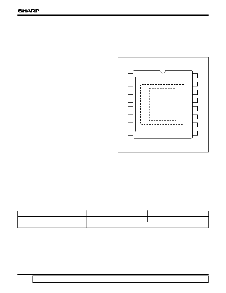
∑ Package :
16-pin shrink-pitch WDIP [Ceramic]
(WDIP016-N-0500C)
Row space : 12.70 mm
COMPARISON TABLE
PIN CONNECTIONS
PRECAUTIONS
∑ The exit pupil position of lens should be more
than 25 mm (LZ2313H5)/20 mm (LZ2314HJ)
from the top surface of the CCD.
∑ Refer to "PRECAUTIONS FOR CCD AREA
SENSORS" for details.
LZ2313H5/LZ2314HJ
LZ2313H5/
LZ2314HJ
1/3-type CCD Area Sensors
with 270 k Pixels
1
OD
2
ÿ
RS
3
RD
4
OS
5
NC
1
6
NC
2
7
ÿ
H2
8
16
15
14
13
12
11
10
9
ÿ
H1
GND
ÿ
V4
ÿ
V3
ÿ
V2
ÿ
V1
PW
OFD
T
1
16-PIN SHRINK-PITCH WDIP
TOP VIEW
(WDIP016-N-0500C)
Characteristics
TV standard
LZ2314HJ
EIA standard (B/W)
LZ2313H5
NTSC standard (Color)
Refer to each following specification.
LZ2313H5/LZ2314HJ
2
PIN DESCRIPTION
ABSOLUTE MAXIMUM RATINGS
(T
A
= +25 ∞C)
SYMBOL
PIN NAME
RD
Reset transistor drain
OD
Output transistor drain
OS
Output signals
ÿ
RS
Reset transistor clock
ÿ
V1
, ÿ
V2
, ÿ
V3
, ÿ
V4
Vertical shift register clock
ÿ
H1
, ÿ
H2
Horizontal shift register clock
OFD
Overflow drain
PW
P-well
GND
Ground
T
1
Test pin
NC
1
, NC
2
No connection
PARAMETER
SYMBOL
RATING
UNIT
Output transistor drain voltage
V
OD
0 to +18
V
Reset transistor drain voltage
V
RD
0 to +18
V
Overflow drain voltage
V
OFD
0 to +55
V
Test pin, T
1
V
T1
0 to +18
V
Reset gate clock voltage
V
ÿRS
≠0.3 to +18
V
Vertical shift register clock voltage
V
ÿV
≠9.0 to +18
V
Horizontal shift register clock voltage
V
ÿH
≠0.3 to +18
V
Voltage difference between P-well and vertical clock
V
PW
-V
ÿV
≠27 to 0
V
Storage temperature
T
STG
≠40 to +85
∞C
Ambient operating temperature
T
OPR
≠20 to +70
∞C
1
NOTE
NOTE :
1. The OFD clock ÿOFD is excluded.
3
LZ2313H5/LZ2314HJ
RECOMMENDED OPERATING CONDITIONS
PARAMETER
SYMBOL
MIN.
TYP.
MAX.
UNIT
NOTE
Ambient operating temperature
T
OPR
25.0
∞C
Output transistor drain voltage
V
OD
14.5
15.0
16.0
V
Reset transistor drain voltage
V
RD
V
OD
V
Overflow drain
voltage
When DC is applied
V
OFD
5.0
19.0
V
1
When pulse is applied p-p level
V
ÿOFD
21.5
V
2
Ground
GND
0.0
V
P-well voltage
V
PW
≠9.0
V
ÿVL
V
Test pin, T
1
V
T1
V
OD
V
Vertical shift
register clock
LOW level
V
ÿV1L
, V
ÿV2L
V
ÿV3L
, V
ÿV4L
≠8.5
≠8.0
≠7.5
V
INTERMEDIATE level
V
ÿV1I
, V
ÿV2I
V
ÿV3I
, V
ÿV4I
0.0
V
HIGH level
V
ÿV1H
, V
ÿV3H
14.5
15.0
17.0
V
Horizontal shift
register clock
LOW level
V
ÿH1L
, V
ÿH2L
≠0.05
0.0
0.05
V
HIGH level
V
ÿH1H
, V
ÿH2H
4.7
5.0
6.0
V
Reset gate clock
LOW level
V
ÿRSL
0.0
V
RD
≠ 13.0
V
HIGH level
V
ÿRSH
V
RD
≠ 8.5
9.5
V
Vertical shift register clock frequency
f
ÿV1
, f
ÿV2
f
ÿV3
, f
ÿV4
15.73
kHz
Horizontal shift register clock frequency
f
ÿH1
, f
ÿH2
9.53
MHz
Reset gate clock frequency
f
ÿRS
9.53
MHz
LZ2313H5
LZ2314HJ
4.5
NOTES :
∑ Connect NC
1
and NC
2
to GND directly or through a capacitor larger than 0.047 µF.
1. When DC voltage is applied, shutter speed is 1/60-second.
2. When pulse is applied, shutter speed is less than 1/60-second.
* To apply power, first connect GND and then turn on V
OFD
. After turning on V
OFD
, turn on PW first and then turn on other
powers and pulses. Do not connect the device to or disconnect it from the plug socket while power is being applied.

LZ2313H5/LZ2314HJ
4
CHARACTERISTICS FOR LZ2313H5
(Drive method : Field accumulation)
(T
A
= +25 ∞C, Operating conditions : The typical values specified in "RECOMMENDED OPERATING CONDITIONS".
Color temperature of light source : 3 200 K, IR cut-off filter (CM-500, 1 mmt) is used.)
PARAMETER
SYMBOL
MIN.
TYP.
MAX.
UNIT
NOTE
Standard output voltage
V
O
150
mV
2
Photo response non-uniformity
PRNU
15
%
3
Saturation output voltage
V
SAT
700
mV
4
Dark output voltage
V
DARK
0.3
3.0
mV
1, 5
Dark signal non-uniformity
DSNU
0.6
2.0
mV
1, 6
Sensitivity
R
440
600
mV
7
Smear ratio
SMR
≠81
≠76
dB
8
Image lag
AI
1.0
%
9
Blooming suppression ratio
ABL
100
10
Output transistor drain current
I
OD
4.0
8.0
mA
Output impedance
R
O
350
$
Vector breakup
5.0
∞, %
11
Line crawling
3.0
%
12
Luminance flicker
2.0
%
13
NOTES :
∑ V
OFD
should be adjusted to the minimum voltage such
that ABL satisfy the specification, or to the value
displayed on the device.
1. T
A
= +60 ∞C
2. The average output voltage under uniform illumination.
The standard exposure conditions are defined as when
Vo is 150 mV.
3. The image area is divided into 10 x 10 segments under
the standard exposure conditions. Each segment's
voltage is the average output voltage of all pixels within
the segment. PRNU is defined by (Vmax ≠ Vmin)/Vo,
where Vmax and Vmin are the maximum and minimum
values of each segment's voltage respectively.
4. The output voltage measured at the carrier peak when
the carrier signal reaches maximum.
5. The average output voltage under non-exposure
conditions.
6. The image area is divided into 10 x 10 segments under
non-exposure conditions. DSNU is defined by (Vdmax ≠
Vdmin), where Vdmax and Vdmin are the maximum and
minimum values of each segment's voltage respectively.
7. The average output voltage when a 1 000 lux light
source with a 90% reflector is imaged by a lens of F4,
f50 mm.
8. The sensor is exposed only in the central area of V/10
square with a lens at F4, where V is the vertical image
size. SMR is defined by the ratio of the output voltage
detected during the vertical blanking period to the
maximum output voltage in the V/10 square.
9. The sensor is exposed at the exposure level
corresponding to the standard conditions. AI is defined
by the ratio of the output voltage measured at the 1st
field during the non-exposure period to the standard
output voltage.
10. The sensor is exposed only in the central area of V/10
square, where V is the vertical image size. ABL is
defined by the ratio of the exposure at the standard
conditions to the exposure at a point where blooming is
observed.
11. Observed with a vector scope when the color bar chart
is imaged under the standard exposure conditions.
12. The difference between the average output voltage of the
(Mg + Ye), (G + Cy) line and that of the (Mg + Cy), (G +
Ye) line under the standard exposure conditions.
13. The difference between the average output voltage of
the odd field and that of the even field under the
standard exposure conditions.

5
LZ2313H5/LZ2314HJ
CHARACTERISTICS FOR LZ2314HJ
(Drive method : Field accumulation)
(T
A
= +25 ∞C, Operating conditions : The typical values specified in "RECOMMENDED OPERATING CONDITIONS".
Color temperature of light source : 3 200 K, IR cut-off filter (CM-500, 1 mmt) is used.)
PARAMETER
SYMBOL
MIN.
TYP.
MAX.
UNIT
NOTE
Standard output voltage
V
O
150
mV
2
Photo response non-uniformity
PRNU
10
%
3
Saturation output voltage
V
SAT
700
mV
4
Dark output voltage
V
DARK
0.3
3.0
mV
1, 5
Dark signal non-uniformity
DSNU
0.6
2.0
mV
1, 6
Sensitivity
R
560
800
mV
7
Smear ratio
SMR
≠90
≠76
dB
8
Image lag
AI
1.0
%
9
Blooming suppression ratio
ABL
100
10
Output transistor drain current
I
OD
4.0
8.0
mA
Output impedance
R
O
350
$
NOTES :
∑ V
OFD
should be adjusted to the minimum voltage such
that ABL satisfy the specification, or to the value
displayed on the device.
1. T
A
= +60 ∞C
2. The average output voltage under uniform illumination.
The standard exposure conditions are defined as when
Vo is 150 mV.
3. The image area is divided into 10 x 10 segments under
the standard exposure conditions. Each segment's
voltage is the average output voltage of all pixels within
the segment. PRNU is defined by (Vmax ≠ Vmin)/Vo,
where Vmax and Vmin are the maximum and minimum
values of each segment's voltage respectively.
4. The image area is divided into 10 x 10 segments. Each
segment's voltage is the average output voltage of all
pixels within the segment. V
SAT
is the minimum
segment's voltage under 10 times exposure of the
standard exposure conditions.
5. The average output voltage under non-exposure
conditions.
6. The image area is divided into 10 x 10 segments under
non-exposure conditions. DSNU is defined by (Vdmax ≠
Vdmin), where Vdmax and Vdmin are the maximum and
minimum values of each segment's voltage respectively.
7. The average output voltage when a 1 000 lux light
source with a 90% reflector is imaged by a lens of F4,
f50 mm.
8. The sensor is exposed only in the central area of V/10
square with a lens at F4, where V is the vertical image
size. SMR is defined by the ratio of the output voltage
detected during the vertical blanking period to the
maximum output voltage in the V/10 square.
9. The sensor is exposed at the exposure level
corresponding to the standard conditions. AI is defined
by the ratio of the output voltage measured at the 1st
field during the non-exposure period to the standard
output voltage.
10. The sensor is exposed only in the central area of V/10
square, where V is the vertical image size. ABL is
defined by the ratio of the exposure at the standard
conditions to the exposure at a point where blooming is
observed.
LZ2313H5/LZ2314HJ
6
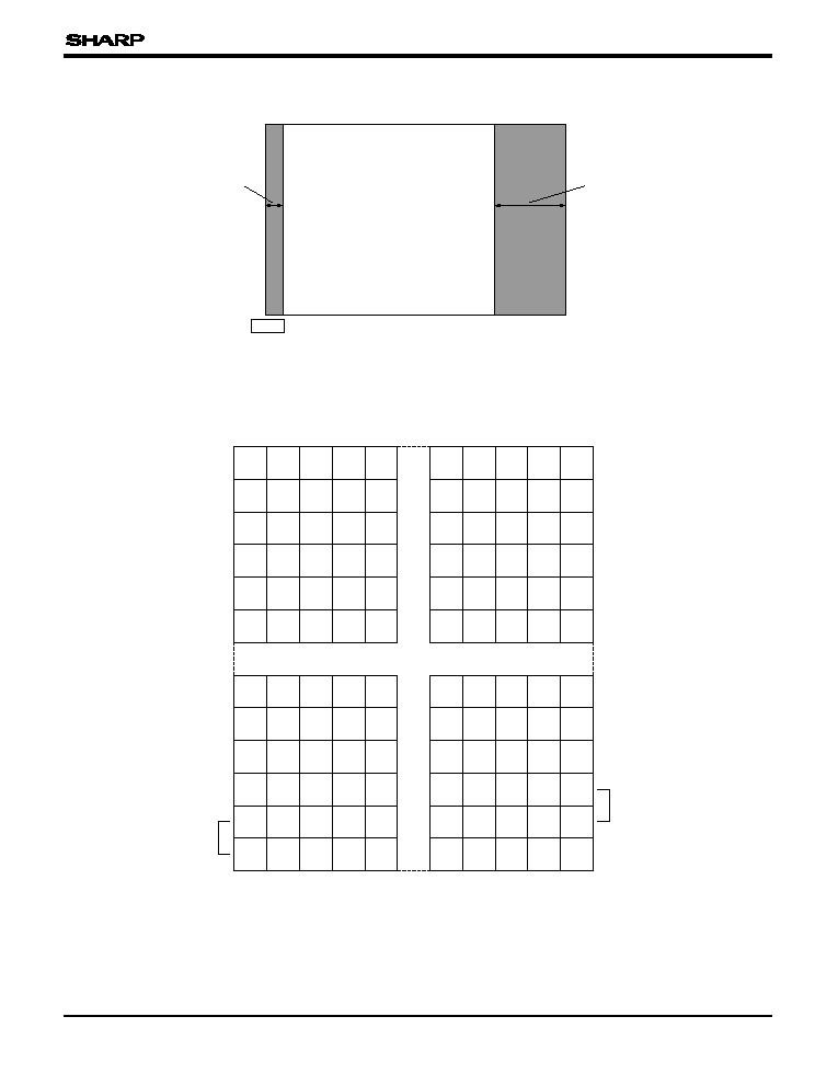
PIXEL STRUCTURE
512 (H) x 492 (V)
1 pin
OPTICAL BLACK
(2 PIXELS)
OPTICAL BLACK
(28 PIXELS)
COLOR FILTER ARRAY (FOR LZ2313H5)
Mg
G
Mg
G
Mg
Cy
Ye
Cy
Ye
Cy
G
Mg
G
Mg
G
Cy
Ye
Cy
Ye
Cy
Mg
G
Mg
G
Mg
Cy
Ye
Cy
Ye
Cy
Mg
G
Mg
G
Mg
Ye
Cy
Ye
Cy
Ye
G
Mg
G
Mg
G
Ye
Cy
Ye
Cy
Ye
Mg
G
Mg
G
Mg
Ye
Cy
Ye
Cy
Ye
G
Mg
G
Mg
G
Ye
Cy
Ye
Cy
Ye
Mg
G
Mg
G
Mg
Ye
Cy
Ye
Cy
Ye
G
Mg
G
Mg
G
Ye
Cy
Ye
Cy
Ye
G
Mg
G
Mg
G
Cy
Ye
Cy
Ye
Cy
Mg
G
Mg
G
Mg
Cy
Ye
Cy
Ye
Cy
G
Mg
G
Mg
G
Cy
Ye
Cy
Ye
Cy
(1, 492)
(512, 492)
(1, 1)
(512, 1)
EVEN
field
ODD
field
LZ2313H5/LZ2314HJ
7
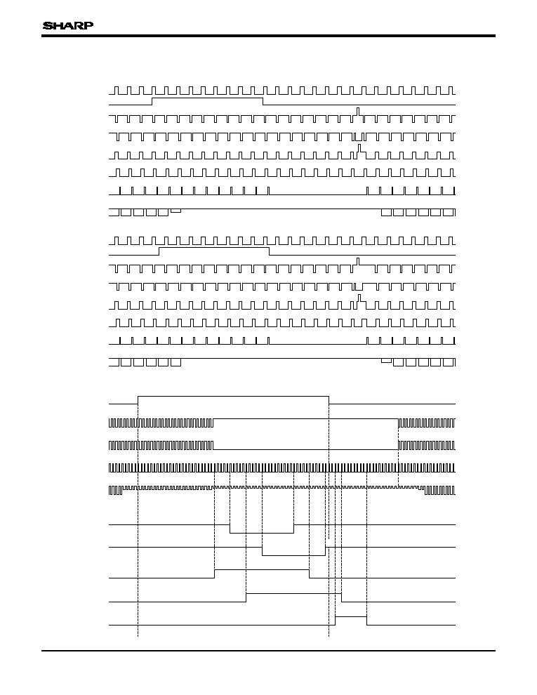
TIMING CHART
484
+
485
486
+
487
488
+
489
490
+
491
492
1
+
2
3
+
4
5
+
6
7
+
8
9
+
10
11
+
12
OS
ÿ
OFD
ÿ
V4
ÿ
V3
ÿ
V2
ÿ
V1
VD
HD
(ODD FIELD)
Shutter speed
1/2 000 s
VERTICAL TRANSFER TIMING
483
+
484
485
+
486
487
+
488
489
+
490
491
+
492
1
2
+
3
4
+
5
6
+
7
8
+
9
10
+
11
OS
ÿ
OFD
ÿ
V4
ÿ
V3
ÿ
V2
ÿ
V1
VD
HD
(EVEN FIELD)
HORIZONTAL TRANSFER TIMING
OS
ÿ
RS
ÿ
H2
ÿ
H1
HD
...512
OB (28)
OB (2)
ÿ
OFD
ÿ
V4
ÿ
V3
ÿ
V2
ÿ
V1
29
606, 1
60
24
54
34
64
62
72
49
39
59
OUTPUT (512) 1
8
READOUT TIMING
ÿ
V4
ÿ
V3
ÿ
V2
ÿ
V1
HD
(ODD FIELD)
(EVEN FIELD)
READOUT TIMING
ÿ
V4
ÿ
V3
ÿ
V2
ÿ
V1
HD
1
29
39
24
34
64
54
59
161
180
290
338
242
290
449
606, 1
60
29
39
54
64
34
59
49
49
60
1
29
39
24
34
64
54
59
161
180
290
338
242
290
606, 1
60
54
64
450
59
49
60
LZ2313H5/LZ2314HJ
LZ2313H5/LZ2314HJ
9
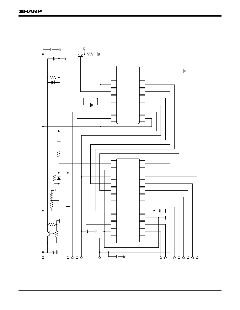
SYSTEM CONFIGURATION EXAMPLE
OD
OS
RD
OFD
PW
ÿ
RS
ÿ
H2
ÿ
H1
GND
ÿ
V4
ÿ
V3
ÿ
V2
ÿ
V1
NC
2
NC
1
T
1
V
3B
V
3A
V
1B
V
1A
V
Ma
V
H
V
4
V
2
V
L
V
Mb
POFD
NC
V
H
V
L
(V
PW
)
V
4X
V
OD
V
3X
V
2X
V
1X
VH
3AX
VH
1AX
+5 V
OFDX
ÿ
H1
ÿ
H2
ÿ
RS
CCD
OUT
100 k$
100 $
1 M$
0.1 µF
1 000 pF
1 000 pF
+
LZ2313H5
or
LZ2314HJ
+
+
V
OFDH
VH
3BX
OFDX
V
2X
V
1X
V
3X
V
DD
GND
V
4X
VH
3AX
VH
1BX
VH
1AX
+
+
+
1
2
3
4
5
6
7
8
12
24
23
22
21
20
19
18
17
13
11
14
10
15
9
16
1
2
3
4
5
6
7
8
16
15
14
13
12
11
10
9
LR36685
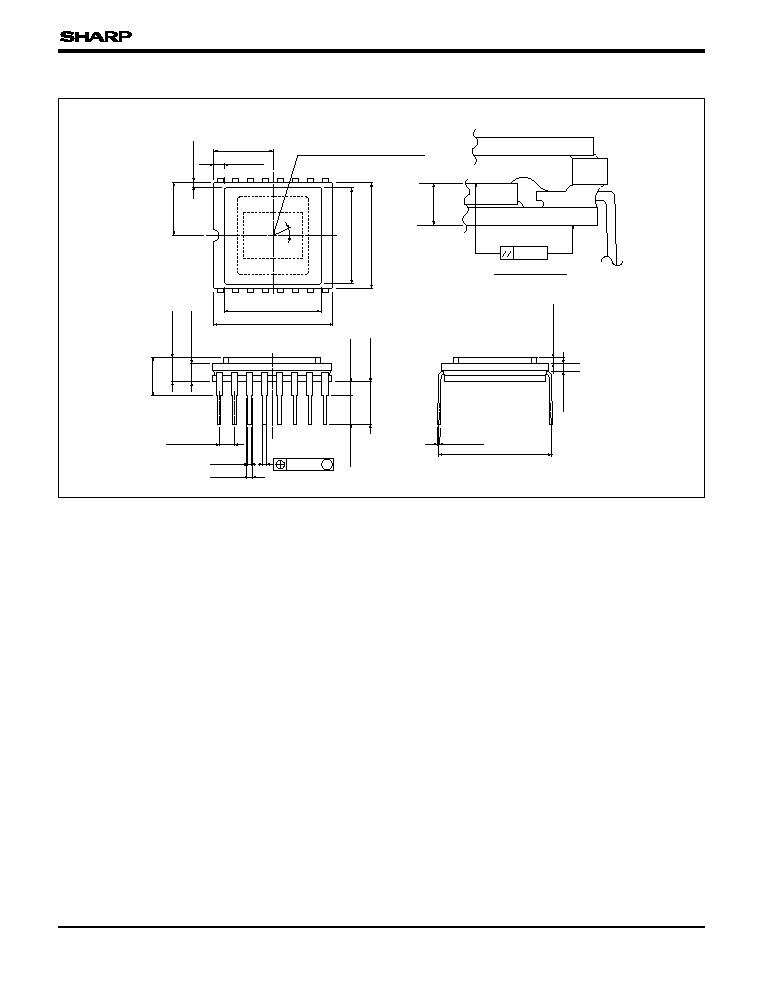
PACKAGES FOR CCD AND CMOS DEVICES
10
PACKAGE
(Unit : mm)
0.04
1.66
±0.10
Package (Cerdip)
Glass Lid
CCD
Cross Section A-A'
1
8
14.00
±0.15
16
9
11.20
±0.10
()
12.40
±0.15
6.20
±0.15
0.60
±0.60
7.00
±0.15
1.40
±0.60
CCD
( : Lid's size)
11.20
±0.10
()
Center of effective imaging area
and center of package
0.25
±0.10
12.70
±0.25
0.80
±0.05
()
1.05
MIN.
0.46
TYP.
0.90
TYP.
2.63
TYP.
5.24
MAX.
3.42
±0.25
1.27
±0.25
3.90
±0.30
2.60
±0.20
P-1.78
TYP.
A'
A
Rotation error of die : ¨ = 1.5∞
MAX.
M
0.25
16 WDIP (WDIP016-N-0500C)
PRECAUTIONS FOR CCD AREA SENSORS
1. Package Breakage
In order to prevent the package from being broken,
observe the following instructions :
1) The CCD is a precise optical component and
the package material is ceramic or plastic.
Therefore,
¯ Take care not to drop the device when
mounting, handling, or transporting.
¯ Avoid giving a shock to the package.
Especially when leads are fixed to the socket
or the circuit board, small shock could break
the package more easily than when the
package isn't fixed.
2) When applying force for mounting the device or
any other purposes, fix the leads between a
joint and a stand-off, so that no stress will be
given to the jointed part of the lead. In addition,
when applying force, do it at a point below the
stand-off part.
(In the case of ceramic packages)
≠ The leads of the package are fixed with low
melting point glass, so stress added to a
lead could cause a crack in the low melting
point glass in the jointed part of the lead.
(In the case of plastic packages)
≠ The leads of the package are fixed with
package body (plastic), so stress added to a
lead could cause a crack in the package
body (plastic) in the jointed part of the lead.
3) When mounting the package on the housing,
be sure that the package is not bent.
≠ If a bent package is forced into place
between a hard plate or the like, the pack-
age may be broken.
4) If any damage or breakage occurs on the sur-
face of the glass cap, its characteristics could
deteriorate.
Therefore,
¯ Do not hit the glass cap.
¯ Do not give a shock large enough to cause
distortion.
¯
Do not scrub or scratch the glass surface.
≠ Even a soft cloth or applicator, if dry, could
cause dust to scratch the glass.
2. Electrostatic Damage
As compared with general MOS-LSI, CCD has
lower ESD. Therefore, take the following anti-static
measures when handling the CCD :
1) Always discharge static electricity by grounding
the human body and the instrument to be used.
To ground the human body, provide resistance
of about 1 M$ between the human body and
the ground to be on the safe side.
2) When directly handling the device with the
fingers, hold the part without leads and do not
touch any lead.
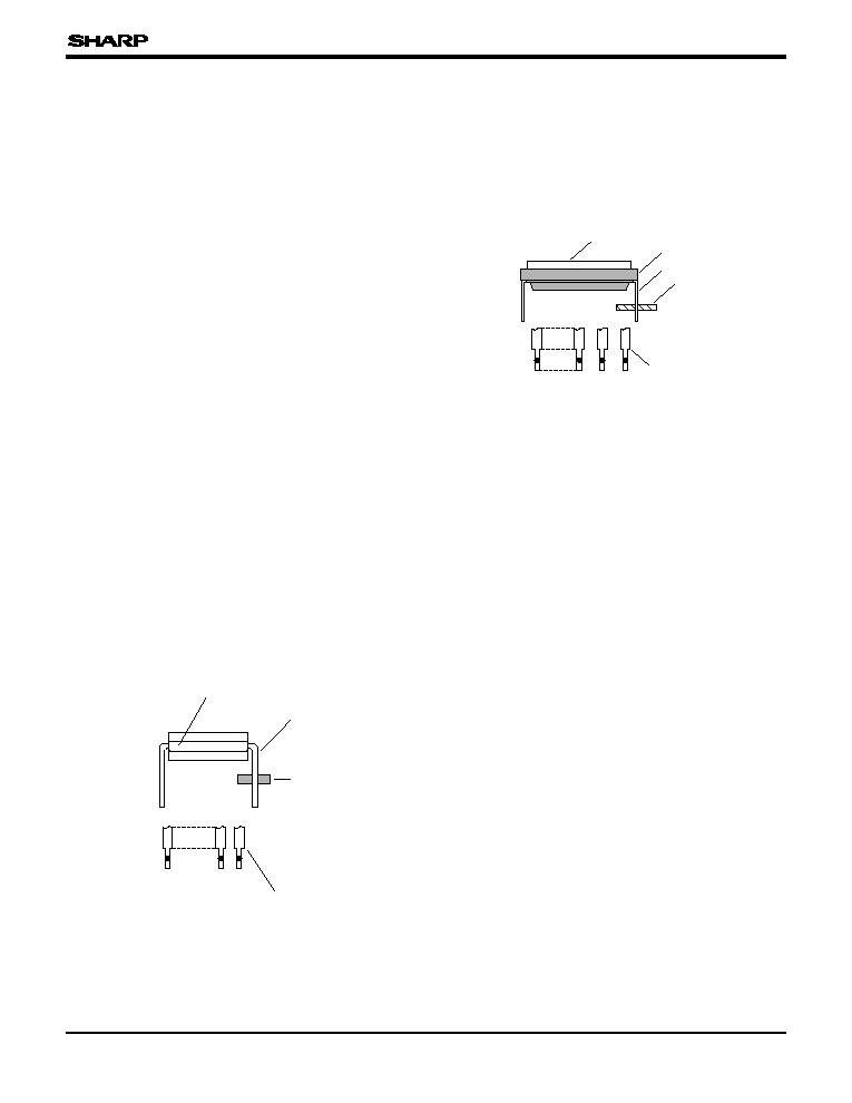
Glass cap
Package
Lead
Fixed
Stand-off
Fixed
Lead
Stand-off
Low melting point glass
11
PRECAUTIONS FOR CCD AREA SENSORS

3) To avoid generating static electricity,
a. do not scrub the glass surface with cloth or
plastic.
b. do not attach any tape or labels.
c. do not clean the glass surface with dust-
cleaning tape.
4) When storing or transporting the device, put it in
a container of conductive material.
3. Dust and Contamination
Dust or contamination on the glass surface could
deteriorate the output characteristics or cause a
scar. In order to minimize dust or contamination on
the glass surface, take the following precautions :
1) Handle the CCD in a clean environment such
as a cleaned booth. (The cleanliness level
should be, if possible, class 1 000 at least.)
2) Do not touch the glass surface with the fingers.
If dust or contamination gets on the glass
surface, the following cleaning method is
recommended :
¯ Dust from static electricity should be blown
off with an ionized air blower. For anti-
electrostatic measures, however, ground all
the leads on the device before blowing off
the dust.
¯
The contamination on the glass surface
should be wiped off with a clean applicator
soaked in Isopropyl alcohol. Wipe slowly and
gently in one direction only.
≠ Frequently replace the applicator and do not
use the same applicator to clean more than
one device.
Note : In most cases, dust and contamination
are unavoidable, even before the device
is first used. It is, therefore, recommended
that the above procedures should be
taken to wipe out dust and contamination
before using the device.
4. Other
1) Soldering should be manually performed within
5 seconds at 350 ∞C maximum at soldering iron.
2) Avoid using or storing the CCD at high tem-
perature or high humidity as it is a precise
optical component. Do not give a mechanical
shock to the CCD.
3) Do not expose the device to strong light. For
the color device, long exposure to strong light
will fade the color of the color filters.
12
PRECAUTIONS FOR CCD AREA SENSORS