 | –≠–ª–µ–∫—Ç—Ä–æ–Ω–Ω—ã–π –∫–æ–º–ø–æ–Ω–µ–Ω—Ç: LZ23H3V1 | –°–∫–∞—á–∞—Ç—å:  PDF PDF  ZIP ZIP |
Document Outline
- ˛ˇ
- ˛ˇ
- ˛ˇ
- ˛ˇ
- ˛ˇ
- ˛ˇ
- ˛ˇ
- ˛ˇ
- ˛ˇ
- ˛ˇ
- ˛ˇ
- ˛ˇ
- ˛ˇ
- ˛ˇ
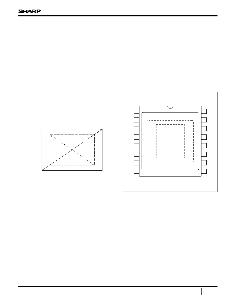
LZ23H3V1
DESCRIPTION
The LZ23H3V1 is a 1/3-type (6.0 mm) solid-state
image sensor that consists of PN photo-diodes
and CCDs (charge-coupled devices). With
approximately 1 090 000 pixels (1 217 horizontal x
893 vertical), the sensor provides a stable high-
resolution color image.
FEATURES
∑ Optical size :
Number of effective pixels
≠ Approx. 1 000 k; 6.6 mm
≠ Approx. 790 k; 5.9 mm (compatible with XGA
format)
∑ Interline scan format
∑ Square pixel
∑ Number of effective pixels : 1 174 (H) x 884 (V)
∑ Number of optical black pixels
≠ Horizontal : 3 front and 40 rear
≠ Vertical : 7 front and 2 rear
∑ Number of dummy bits
≠ Horizontal : 22
≠ Vertical : 2
∑ Pixel pitch : 4.6 µm (H) x 4.6 µm (V)
∑ R, G, and B primary color mosaic filters
∑ Supports monitoring mode
∑ Low fixed-pattern noise and lag
∑ No burn-in and no image distortion
∑ Blooming suppression structure
∑ Built-in output amplifier
∑ Built-in overflow drain voltage circuit and reset
gate voltage circuit
∑ Variable electronic shutter
∑ Package :
16-pin shrink-pitch WDIP [Ceramic]
(WDIP016-N-0500C)
Row space : 12.70 mm
PIN CONNECTIONS
PRECAUTIONS
∑ The exit pupil position of lens should be 15 to 50
mm from the top surface of the CCD.
∑ Refer to "PRECAUTIONS FOR CCD AREA
SENSORS" for details.
(1 024)
1 000 k pixels
1 156
790 k pixels
866
(768)
(5.9 mm)
6.6 mm
In the absence of confirmation by device specification sheets, SHARP takes no responsibility for any defects that may occur in equipment using any SHARP devices shown in
catalogs, data books, etc. Contact SHARP in order to obtain the latest device specification sheets before using any SHARP device.
1
LZ23H3V1
1/3-type Interline Color CCD Area
Sensor with 1 090 k Pixels
1
OD
2
GND
3
OFD
4
PW
5
ÿ
RS
6
NC
7
ÿ
H1
8
16
15
14
13
12
11
10
9
ÿ
H2
OS
GND
ÿ
V1A
ÿ
V1B
ÿ
V2
ÿ
V3A
ÿ
V3B
ÿ
V4
16-PIN SHRINK-PITCH WDIP
TOP VIEW
(WDIP016-N-0500C)
LZ23H3V1
2
PIN DESCRIPTION
SYMBOL
PIN NAME
OD
Output transistor drain
OS
Output signals
ÿ
RS
Reset transistor clock
ÿ
V1A
, ÿ
V1B
, ÿ
V2
, ÿ
V3A
, ÿ
V3B
, ÿ
V4
Vertical shift register clock
ÿ
H1
, ÿ
H2
Horizontal shift register clock
PW
P-well
GND
Ground
NC
No connection
Overflow drain
OFD
ABSOLUTE MAXIMUM RATINGS
(T
A
= +25 ∞C)
PARAMETER
SYMBOL
RATING
UNIT
Output transistor drain voltage
V
OD
0 to +18
V
Reset gate clock voltage
V
ÿRS
Internal output
V
Vertical shift register clock voltage
V
ÿV
V
PW
to +18
V
Horizontal shift register clock voltage
V
ÿH
≠0.3 to +12
V
Voltage difference between P-well and vertical clock
V
PW
-V
ÿV
≠29 to 0
V
Storage temperature
T
STG
≠40 to +85
∞C
Ambient operating temperature
T
OPR
≠20 to +70
∞C
2
NOTE
NOTES :
1. Do not connect to DC voltage directly. When OFD is connected to GND, connect V
OD
to GND. Overflow drain clock is
applied below 27 Vp-p.
2. Do not connect to DC voltage directly. When ÿ
RS
is connected to GND, connect V
OD
to GND. Reset gate clock is
applied below 8 Vp-p.
3. When clock width is below 10 µs, and clock duty factor is below 0.1%, voltage difference between vertical clocks will be
below 28 V.
1
V
Internal output
V
OFD
Overflow drain voltage
3
V
0 to +15
V
ÿV
-V
ÿV
Voltage difference between vertical clocks

LZ23H3V1
3
RECOMMENDED OPERATING CONDITIONS
PARAMETER
SYMBOL
MIN.
TYP.
MAX.
UNIT
NOTE
Ambient operating temperature
T
OPR
25.0
∞C
Output transistor drain voltage
V
OD
14.55
15.0
15.45
V
NOTES :
1. Use the circuit parameter indicated in "SYSTEM CONFIGURATION EXAMPLE", and do not connect to DC voltage directly.
2. V
PW
is set below V
ÿVL
that is low level of vertical shift register clock, or is used with the same power supply that is connected
to V
L
of V driver IC.
3. Operation frequency is 14.32 MHz.
4. Operation frequency is 18.00 MHz.
* To apply power, first connect GND and then turn on V
OD
. After turning on V
OD
, turn on PW first and then turn on other powers
and pulses. Do not connect the device to or disconnect it from the plug socket while power is being applied.
1
V
26.5
24.5
V
ÿOFD
Overflow drain clock
P-well voltage
V
PW
≠10.0
V
ÿVL
V
2
Ground
GND
0.0
V
V
≠8.5
≠9.0
≠9.5
V
ÿV1AL
, V
ÿV1BL
, V
ÿV2L
V
ÿV3AL
, V
ÿV3BL
, V
ÿV4L
Vertical shift
register clock
LOW level
INTERMEDIATE level
HIGH level
V
ÿV1AI
, V
ÿV1BI
, V
ÿV2I
V
ÿV3AI
, V
ÿV3BI
, V
ÿV4I
V
ÿV1AH
, V
ÿV1BH
V
ÿV3AH
, V
ÿV3BH
14.55
0.0
15.0
15.45
V
V
LOW level
Horizontal shift
register clock
V
ÿH1L
, V
ÿH2L
≠0.05
0.0
0.05
V
HIGH level
V
ÿH1H
, V
ÿH2H
4.5
5.0
5.5
V
1
V
5.5
5.0
4.5
V
ÿRS
Reset gate clock p-p level
Reset gate clock frequency
f
ÿRS
14.32
MHz
3
Horizontal shift register clock frequency
f
ÿH1
, f
ÿH2
14.32
MHz
3
Vertical shift register clock frequency
f
ÿV1A
, f
ÿV1B
, f
ÿV2
f
ÿV3A
, f
ÿV3B
, f
ÿV4
10.88
kHz
3
4
kHz
13.47
4
MHz
18.00
4
MHz
18.00
p-p level

LZ23H3V1
4
CHARACTERISTICS
(Drive method : 1/30 s frame accumulation)
(T
A
= +25 ∞C, Operating conditions : The typical values specified in "RECOMMENDED OPERATING CONDITIONS".
Color temperature of light source : 3 200 K, IR cut-off filter (CM-500, 1 mmt) is used.)
PARAMETER
SYMBOL
MIN.
TYP.
MAX.
UNIT
NOTE
Standard output voltage
V
O
150
mV
2
Photo response non-uniformity
PRNU
10
%
3
Saturation output voltage
V
SAT
450
530
mV
4
Dark output voltage
V
DARK
0.5
3.0
mV
1, 6
Dark signal non-uniformity
DSNU
0.5
2.0
mV
1, 7
Sensitivity (green channel)
R
105
150
mV
8
Smear ratio
SMR
≠75
≠65
dB
9
NOTES :
∑ Within the recommended operating conditions of V
OD
,
V
OFD
of the internal output satisfies with ABL larger than
500 times exposure of the standard exposure conditions,
and V
SAT
larger than 330 mV.
1. T
A
= +60 ∞C
2. The average output voltage of G signal under uniform
illumination. The standard exposure conditions are
defined as when Vo is 150 mV.
3. The image area is divided into 10 x 10 segments under
the standard exposure conditions. Each segment's
voltage is the average output voltage of all pixels within
the segment. PRNU is defined by (Vmax ≠ Vmin)/Vo,
where Vmax and Vmin are the maximum and minimum
values of each segment's voltage respectively.
4. The image area is divided into 10 x 10 segments. Each
segment's voltage is the average output voltage of all
pixels within the segment. V
SAT
is the minimum
segment's voltage under 10 times exposure of the
standard exposure conditions. The operation of OFDC is
high. (for still image capturing)
5. The image area is divided into 10 x 10 segments. Each
segment's voltage is the average output voltage of all
pixels within the segment. V
SAT
is the minimum
segment's voltage under 10 times exposure of the
standard exposure conditions. The operation of OFDC is
low.
6. The average output voltage under non-exposure
conditions.
7. The image area is divided into 10 x 10 segments under
non-exposure conditions. DSNU is defined by (Vdmax ≠
Vdmin), where Vdmax and Vdmin are the maximum and
minimum values of each segment's voltage respectively.
8. The average output voltage of G signal when a 1 000
lux light source with a 90% reflector is imaged by a lens
of F4, f50 mm.
9. The sensor is exposed only in the central area of V/10
square with a lens at F4, where V is the vertical image
size. SMR is defined by the ratio of the output voltage
detected during the vertical blanking period to the
maximum output voltage in the V/10 square.
10. The sensor is exposed at the exposure level
corresponding to the standard conditions. AI is defined
by the ratio of the output voltage measured at the 1st
field during the non-exposure period to the standard
output voltage.
11. The sensor is exposed only in the central area of V/10
square, where V is the vertical image size. ABL is
defined by the ratio of the exposure at the standard
conditions to the exposure at a point where blooming is
observed.
12. The sensor is exposed at the exposure level
corresponding to the standard conditions. LCR is defined
by (V
G
/V
O
) x 100, where V
G
is the difference
between the average output voltage of G signal at the
1st field, and that of G signal at the 2nd field.
5
mV
410
330
11
500
ABL
Blooming suppression ratio
10
%
1.0
AI
Image lag
Output transistor drain current
I
OD
4.0
8.0
mA
12
%
3.0
LCR
Line crawling
LZ23H3V1
5
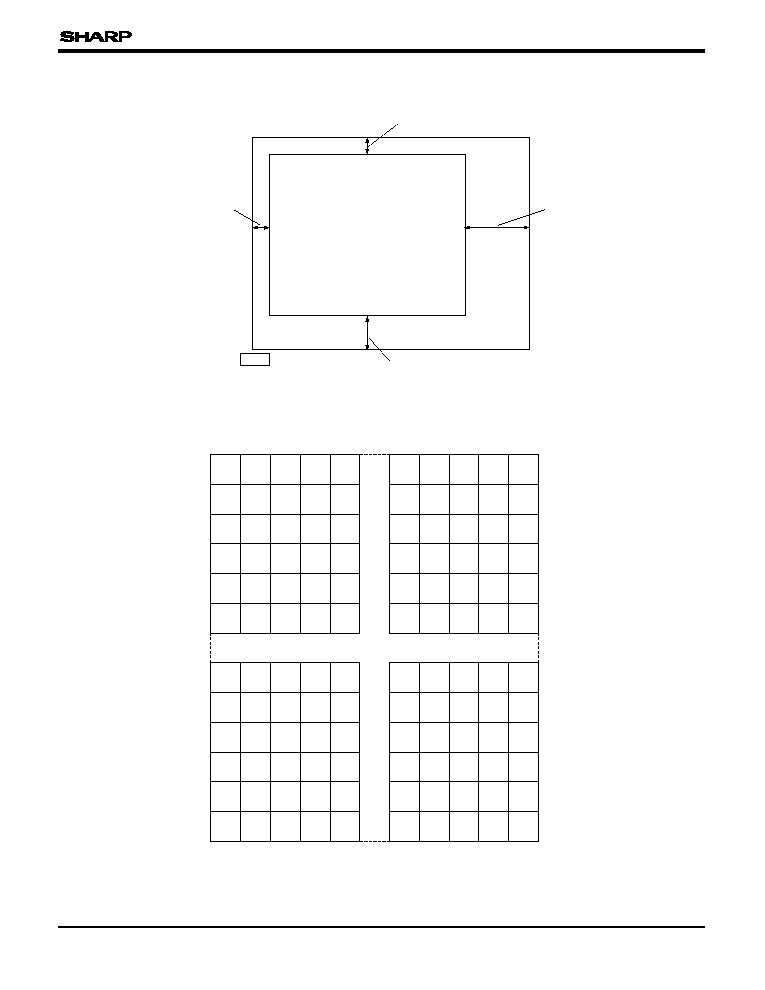
PIXEL STRUCTURE
1 pin
,,,,,,,,,
,,,,,,,,,
,,,,,,,,,
,,,,,,,,,
,,,,,,,,,
,,,,,,,,,
,,,,,,,,,
yyyyyyyyy
yyyyyyyyy
yyyyyyyyy
yyyyyyyyy
yyyyyyyyy
yyyyyyyyy
yyyyyyyyy
,,,,,,,,,
,,,,,,,,,
,,,,,,,,,
,,,,,,,,,
,,,,,,,,,
,,,,,,,,,
,,,,,,,,,
yyyyyyyyy
yyyyyyyyy
yyyyyyyyy
yyyyyyyyy
yyyyyyyyy
yyyyyyyyy
yyyyyyyyy
1 174 (H) x 884 (V)
OPTICAL BLACK
(2 PIXELS)
OPTICAL BLACK
(7 PIXELS)
OPTICAL BLACK
(3 PIXELS)
OPTICAL BLACK
(40 PIXELS)
COLOR FILTER ARRAY
G
B
G
B
G
R
G
R
G
R
G
B
G
B
G
R
G
R
G
R
G
B
G
B
G
R
G
R
G
R
B
G
B
G
B
G
R
G
R
G
B
G
B
G
B
G
R
G
R
G
B
G
B
G
B
G
R
G
R
G
B
G
B
G
B
G
R
G
R
G
B
G
B
G
B
G
R
G
R
G
B
G
B
G
B
G
R
G
R
G
G
B
G
B
G
R
G
R
G
R
G
B
G
B
G
R
G
R
G
R
G
B
G
B
G
R
G
R
G
R
(1, 884)
(1 174, 884)
(1, 1)
(1 174, 1)
ÿ
V3B
ÿ
V1A
ÿ
V1B
ÿ
V3A
ÿ
V1A
ÿ
V1A
ÿ
V3A
ÿ
V1B
ÿ
V3B
ÿ
V1B
ÿ
V3A
ÿ
V3B
Pin arrangement
of the vertical
readout clock
LZ23H3V1
6
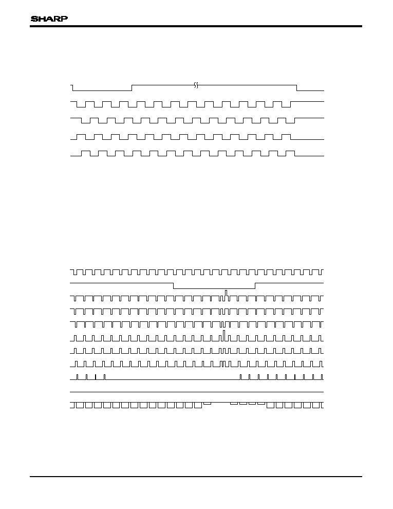
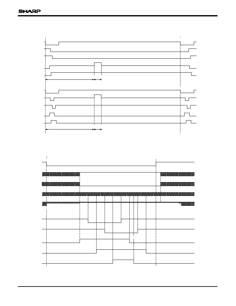
TIMING CHART
NOTES :
1. Do not use these signals immediately after field accumulation mode is transferred to frame
accumulation mode for still image capturing.
2. Do not use these signals immediately after frame accumulation mode is transferred to field
accumulation mode for monitoring mode image.
* Apply at least an OFD shutter pulse to OFD in each field accumulation mode.
* Do not use the field signals immediately after frame accumulation mode is transferred to field
accumulation mode.
ÿ
V3A
ÿ
V2
ÿ
V1B
ÿ
V1A
VD
TIMING CHART EXAMPLE
OS
OFDC
ÿ
OFD
ÿ
V4
ÿ
V3B
(at OFD shutter operation)
Field accumulation mode
Field accumulation
Not for use
(NOTE 1)
Not for use
(NOTE 1)
Not for use
(NOTE 2)
Frame accumulation mode
(2.3..882.883)
(2.3..882.883)
(2.4..882.884)
(1.3..881.883)
mode
(2.3..882.883)
(Number of
vertical line)
Pulse diagram in more detail is shown in the figure q to t after next page.
Field accumulation mode Frame accumulation
mode at first
Frame accumulation mode
Field accumulation
mode at first
Field accumulation
mode
q
q
w
e
r
e'
t
q
ÿ
OFD
ÿ
V3A
OFDC
OS
ÿ
V4
ÿ
V3B
ÿ
V2
ÿ
V1B
ÿ
V1A
VD
HD
Shutter speed
1/1 000 s
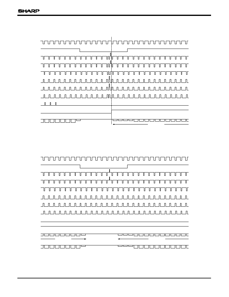
q VERTICAL TRANSFER TIMING FOR 14.3 MHz OPERATION øFIELD ACCUMULATION MODE°
453 1
6
10
874 875 878 879 882 883 OB2
OB1 OB2 OB5 OB6
2
3
6
7
10
11
14
15
18
19
GB RG GB RG GB RG GB RG GB RG
GB RG GB RG GB RG
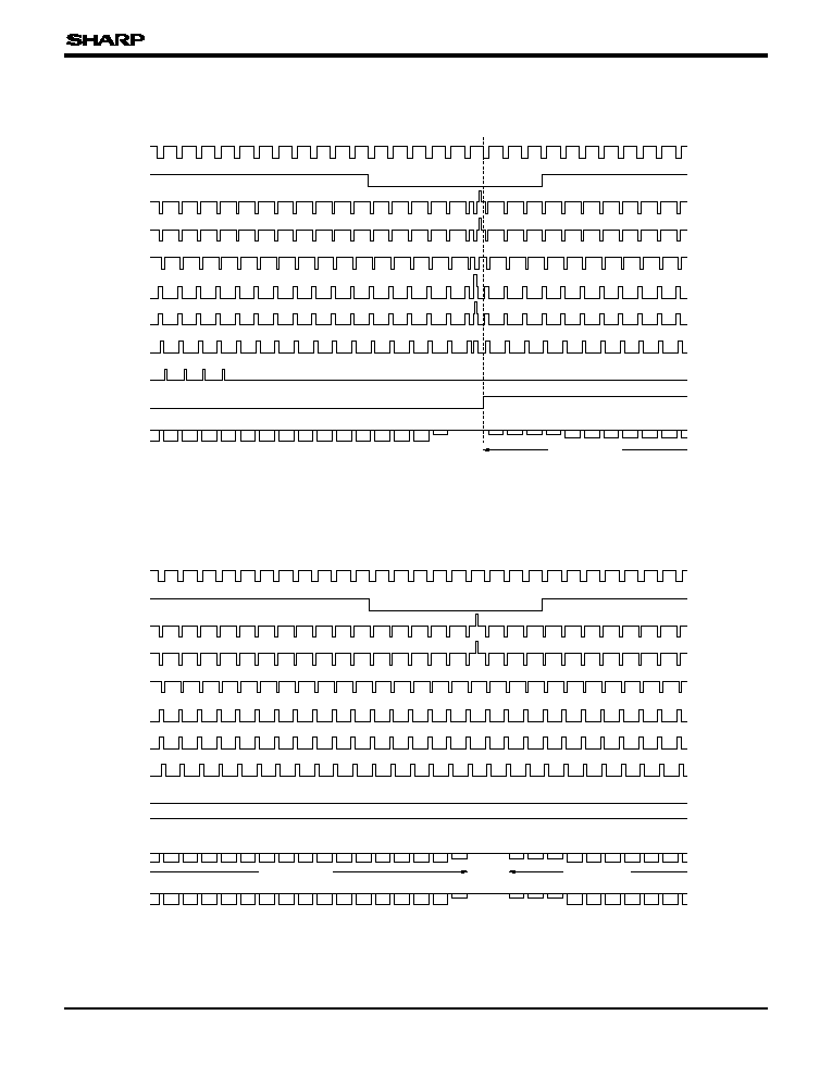
LZ23H3V1
7
ÿ
OFD
ÿ
V3A
OFDC
ÿ
V4
ÿ
V3B
ÿ
V2
ÿ
V1B
ÿ
V1A
VD
HD
(2nd FIELD)
e, e' VERTICAL TRANSFER TIMING FOR 14.3 MHz OPERATION øFRAME ACCUMULATION MODE°
453 454
459
463
OS
e'
872 874 876 878 880 882
OB2 OB4 OB6
1
3
5
7
9
11
13
15
17
19
RG RG RG RG RG RG RG RG RG RG
GB GB GB GB GB GB
884 OB2
GB
Not for use
Not for use
OS
e
ÿ
OFD
ÿ
V3A
OFDC
OS
ÿ
V4
ÿ
V3B
ÿ
V2
ÿ
V1B
ÿ
V1A
VD
HD
Shutter speed
1/1 000 s
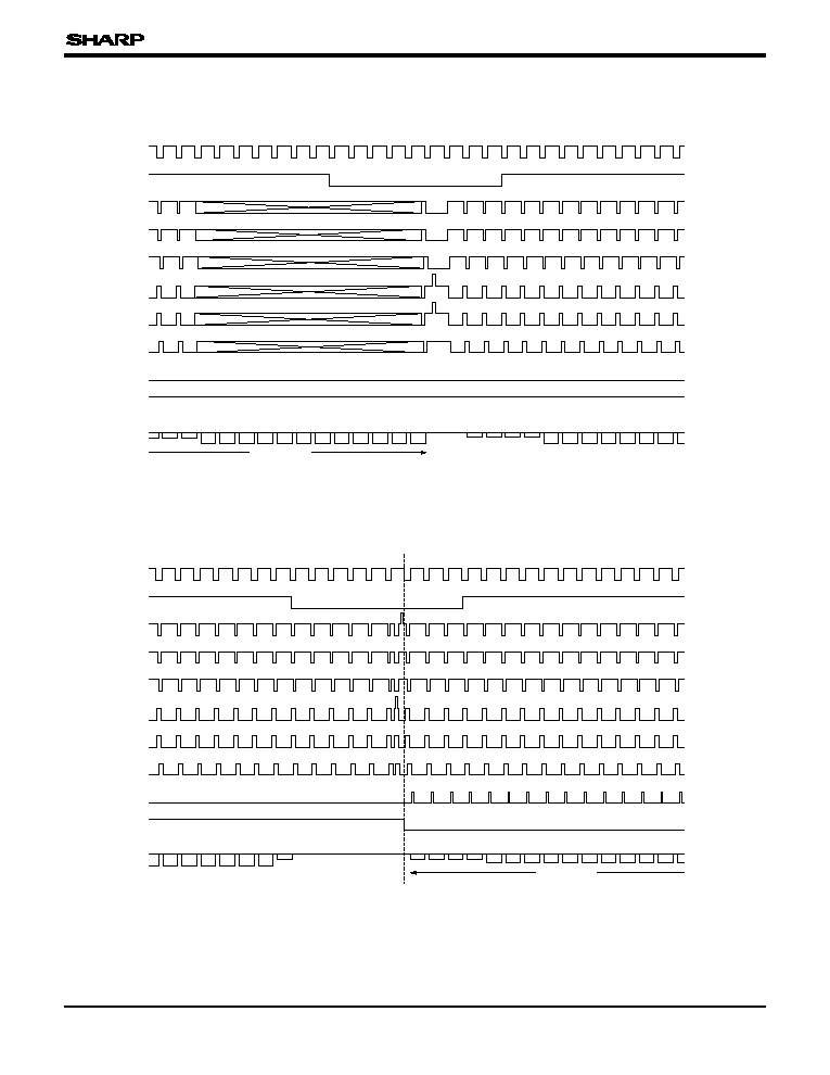
w VERTICAL TRANSFER TIMING FOR 14.3 MHz OPERATION øFRAME ACCUMULATION MODE AT FIRST°
453 1
6
10
874 875 878 879 882 883 OB2
GB RG GB RG GB RG
Not for use
* Do not use the frame signals immediately after field accumulation is transferred to frame
accumulation mode.
* Do not use the frame signals immediately after field accumulation mode is transferred to frame
accumulation mode.
LZ23H3V1
8
ÿ
OFD
ÿ
V3A
OFDC
ÿ
V4
ÿ
V3B
ÿ
V2
ÿ
V1B
ÿ
V1A
VD
HD
(1st FIELD)
r VERTICAL TRANSFER TIMING FOR 14.3 MHz OPERATION øFRAME ACCUMULATION MODE°
906
900
1
6
10
OS
OB1 OB3 OB5 OB7
2
4
6
8
10
12
14
GB GB GB GB GB GB GB
Not for use
Charge swept transfer (658 stages)
ÿ
OFD
ÿ
V3A
OFDC
OS
ÿ
V4
ÿ
V3B
ÿ
V2
ÿ
V1B
ÿ
V1A
VD
HD
Shutter speed
1/1 000 s
t VERTICAL TRANSFER TIMING FOR 14.3 MHz OPERATION øFIELD ACCUMULATION MODE AT FIRST°
906 1
6
10
873 875 877 879 881 883 OB1
RG RG RG RG RG RG
Not for use
* Do not use the frame signals immediately after field accumulation mode is transferred to frame
accumulation mode.
* Do not use the field signals immediately after frame accumulation mode is transferred to field
accumulation mode.
LZ23H3V1
9
ÿ
V3A
ÿ
V3B
ÿ
V4
ÿ
V2
ÿ
V1B
ÿ
V1A
HD
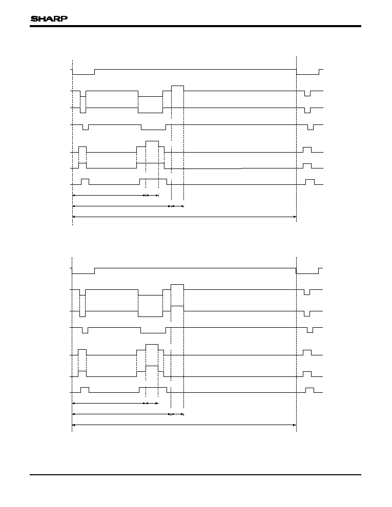
READOUT TIMING FOR 14.3 MHz OPERATION øFIELD ACCUMULATION MODE°
1
1316,
64 96
40
56 104
88
384
436
508
408
132
48 80
392
536
588
660
30.5 µs (436 bits)
41.1 µs (588 bits)
91.9 µs (1 316 bits)
(72 bits)
(72 bits)
1316, 1
5.03 µs
400
560
552
544
5.03 µs
ÿ
V3A
ÿ
V3B
ÿ
V4
ÿ
V2
ÿ
V1B
ÿ
V1A
HD
READOUT TIMING FOR 14.3 MHz OPERATION øFRAME ACCUMULATION MODE AT FIRST°
64 96
40
56 104
88
384
436
508
408
132
48 80
392
536
588
660
30.5 µs (436 bits)
41.1 µs (588 bits)
91.9 µs (1 316 bits)
(72 bits)
(72 bits)
1316, 1
5.03 µs
5.03 µs
400
560
1316, 1
552
544
LZ23H3V1
10
OS
ÿ
RS
ÿ
H2
ÿ
H1
HD
OB (40)
ÿ
OFD
ÿ
V4
ÿ
V2
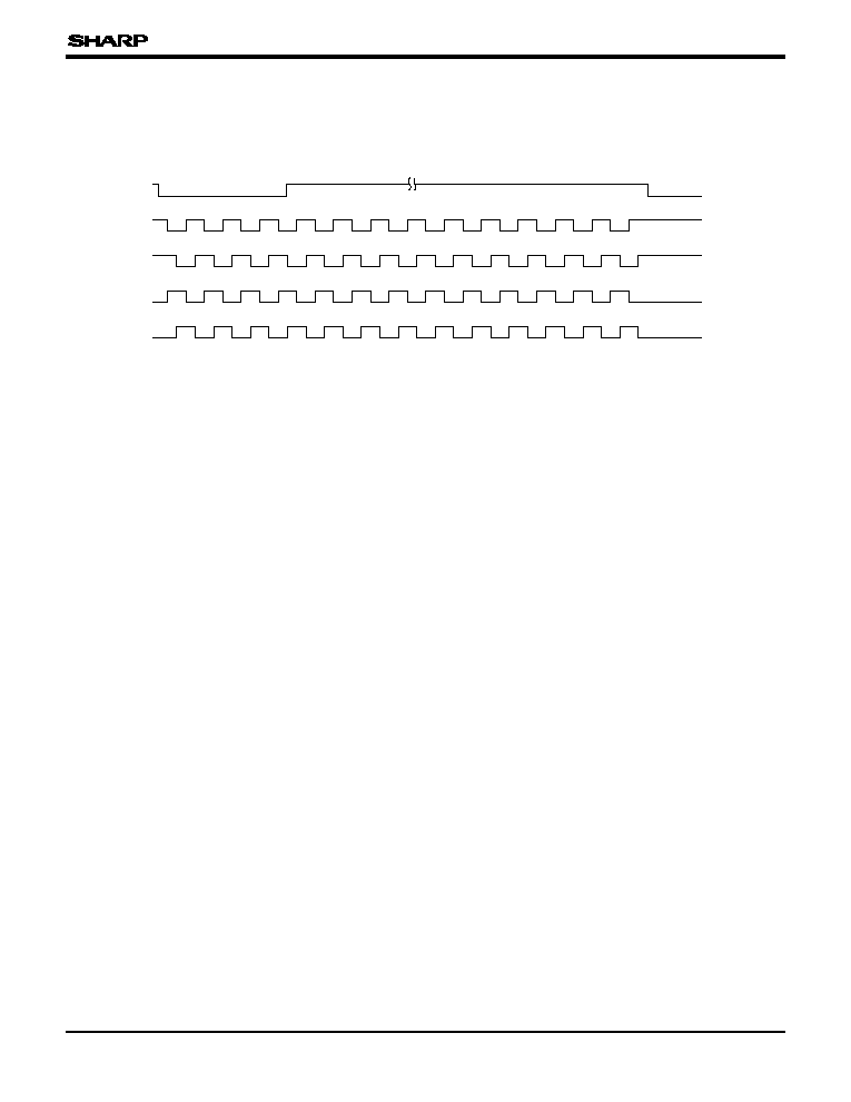
HORIZONTAL TRANSFER TIMING FOR 14.3 MHz OPERATION
1316, 1
132
48
80
64
96
40
56
104
72
92
117.5
40
88
..1174
ÿ
V1A
ÿ
V1B
ÿ
V3A
ÿ
V3B
PRE SCAN (22)
OB (3)
OUTPUT (1 174) 1
ÿ
V4
ÿ
V3A
ÿ
V3B
ÿ
V2
ÿ
V1B
ÿ
V1A
HD
ÿ
V4
ÿ
V2
ÿ
V1B
ÿ
V1A
ÿ
V3B
ÿ
V3A
HD
READOUT TIMING FOR 14.3 MHz OPERATION øFRAME ACCUMULATION MODE°
64
40
56
476
548
132
48
(72 bits)
33.2 µs (476 bits)
80
96
88
104
1
1316, 1
56
40
104
88
132
48 80
64 96
80
96
88
104
48
64
40
56
1
5.03 µs
(72 bits)
33.2 µs (476 bits)
5.03 µs
1316, 1
(1st FIELD)
(2nd FIELD)
476
548
LZ23H3V1
11
ÿ
V1A
ÿ
V1B
ÿ
V4
ÿ
V3A
ÿ
V3B
ÿ
V2
HD
CHARGE SWEPT TRANSFER TIMING FOR 14.3 MHz OPERATION
900H
901H 902H
905H 906H
∑ ∑ ∑ ∑ ∑
1
132
1316
1306
2
14 26 38 50
1306
2
14 26 38 50
1312
8
20 32 44
1312
8
20 32 44
1
2
3
4
∑ ∑ ∑ ∑ ∑ ∑ ∑
658
657
656
1H 2H 3H 4H 5H 6H
ÿ
V4
OFDC
OS
ÿ
V3B
ÿ
V3A
ÿ
V2
ÿ
V1B
ÿ
V1A
VD
HD
Shutter speed
1/1 000 s
q VERTICAL TRANSFER TIMING FOR 18.0 MHz OPERATION øFIELD ACCUMULATION MODE°
ÿ
OFD
442
449 1
6
10
858 859 862 863 866 867 870 871 874 875 878 879 882 883 OB2
2
OB6
OB5
OB2
OB1
3
6
7
10
11
GB RG GB RG GB RG GB RG GB RG GB RG GB RG
GB RG GB RG GB RG
* Do not use the field signals immediately after frame accumulation mode is transferred to field
accumulation mode.
LZ23H3V1
12
ÿ
V4
OFDC
OS
ÿ
V3B
ÿ
V3A
ÿ
V2
ÿ
V1B
ÿ
V1A
VD
HD
Shutter speed
1/1 000 s
w VERTICAL TRANSFER TIMING FOR 18.0 MHz OPERATION øFRAME ACCUMULATION MODE AT FIRST°
ÿ
OFD
442
449 1
6
10
858 859 862 863 866 867 870 871 874 875 878 879 882 883 OB2
GB RG GB RG GB RG GB RG GB RG GB RG GB RG
Not for use
* Do not use the field signals immediately after frame accumulation mode is transferred to field
accumulation mode.
* Do not use the field signals immediately after frame accumulation mode is transferred to field
accumulation mode.
ÿ
V4
OFDC
OS
e
ÿ
V3B
ÿ
V3A
ÿ
V2
ÿ
V1B
ÿ
V1A
VD
HD
e, e' VERTICAL TRANSFER TIMING FOR 18.0 MHz OPERATION øFRAME ACCUMULATION MODE°
ÿ
OFD
449 450
455
459
856 858 860 862 864 866 868 870 872 874 876 878 880 882 884 OB2
1
OB6
OB4
OB2
3
5
7
9
11
GB GB GB GB GB GB GB GB GB GB GB GB GB GB GB
RG RG RG RG RG RG
(2nd FIELD)
Not for use
Not for use
OS
e'
LZ23H3V1
13
ÿ
V4
OFDC
OS
ÿ
V3B
ÿ
V3A
ÿ
V2
ÿ
V1B
ÿ
V1A
VD
HD
r VERTICAL TRANSFER TIMING FOR 18.0 MHz OPERATION øFRAME ACCUMULATION MODE°
ÿ
OFD
888
898 1
6
10
OB7
OB5
OB3
OB1
2
4
6
8
GB GB GB GB
(1st FIELD)
Not for use
Charge swept transfer (668 stages)
ÿ
V4
OFDC
OS
ÿ
V3B
ÿ
V3A
ÿ
V2
ÿ
V1B
ÿ
V1A
VD
HD
Shutter speed
1/1 000 s
t VERTICAL TRANSFER TIMING FOR 18.0 MHz OPERATION øFIELD ACCUMULATION MODE AT FIRST°
ÿ
OFD
898 1
6
10
857 859 861 863 865 867 869 871 873 875 877 879 881 883 OB1
RG RG RG RG RG RG RG RG RG RG RG RG RG RG
Not for use
* Do not use the frame signals immediately after field accumulation mode is transferred to frame
accumulation mode.
* Do not use the field signals immediately after frame accumulation mode is transferred to field
accumulation mode.
LZ23H3V1
14
ÿ
V3A
ÿ
V3B
ÿ
V4
ÿ
V2
ÿ
V1B
ÿ
V1A
HD
READOUT TIMING FOR 18.0 MHz OPERATION øFIELD ACCUMULATION MODE°
1336, 1
50
70
40 100
110
480
660
725
815
680
500
670
470
535 625
1336, 1
90
132
60
490
690
120
29.7 µs (535 bits)
5.00 µs
(90 bits)
5.00 µs
(90 bits)
41.1 µs (588 bits)
74.2 µs (1336 bits)
ÿ
V3A
ÿ
V3B
ÿ
V4
ÿ
V2
ÿ
V1B
ÿ
V1A
HD
READOUT TIMING FOR 18.0 MHz OPERATION øFRAME ACCUMULATION MODE AT FIRST°
50
70
40 100
110
480
660
725
815
680
500
670
470
535 625
1336, 1
90
132
60
490
690
120
1336, 1
29.7 µs (535 bits)
5.00 µs
(90 bits)
5.00 µs
(90 bits)
41.1 µs (588 bits)
74.2 µs (1 336 bits)
LZ23H3V1
15
ÿ
V4
ÿ
V2
HD
(1st FIELD)
(2nd FIELD)
READOUT TIMING FOR 18.0 MHz OPERATION øFRAME ACCUMULATION MODE°
ÿ
V4
ÿ
V2
HD
1
50
70
40
60
90
110
100
120
132
1
90
585 675
110
70
40 100
100
40
120
60
120
60
110
70
90
50
50
132
1336, 1
32.5 µs (585 bits)
585 675
(90 bits)
32.5 µs (585 bits)
(90 bits)
1336, 1
ÿ
V1A
ÿ
V1B
ÿ
V3A
ÿ
V3B
5.00 µs
5.00 µs
ÿ
V1A
ÿ
V1B
ÿ
V3A
ÿ
V3B
OS
ÿ
RS
ÿ
H2
ÿ
H1
HD
OB (40)
OB (3)
PRE SCAN (22)
ÿ
OFD
ÿ
V4
ÿ
V2
HORIZONTAL TRANSFER TIMING FOR 18.0 MHz OPERATION
132
50
90
70
40
60
120
80
105
137.5
40
..1174
110
1336, 1
100
ÿ
V1A
ÿ
V1B
ÿ
V3A
ÿ
V3B
OUTPUT (1 174) 1
LZ23H3V1
16
ÿ
V1A
ÿ
V1B
ÿ
V4
ÿ
V3A
ÿ
V3B
ÿ
V2
HD
CHARGE SWEPT TRANSFER TIMING FOR 18.0 MHz OPERATION
888H
889H
890H
897H
898H 1H
2H
3H
4H
5H 6H
∑ ∑ ∑ ∑ ∑
1
132
1336
1322
2
18 34 50 66
1322
2
18 34 50 66
1330
10 26 42 58
1330
10 26 42 58
1
2
3
4
∑ ∑ ∑ ∑ ∑ ∑ ∑
668
667
666
LZ23H3V1
17
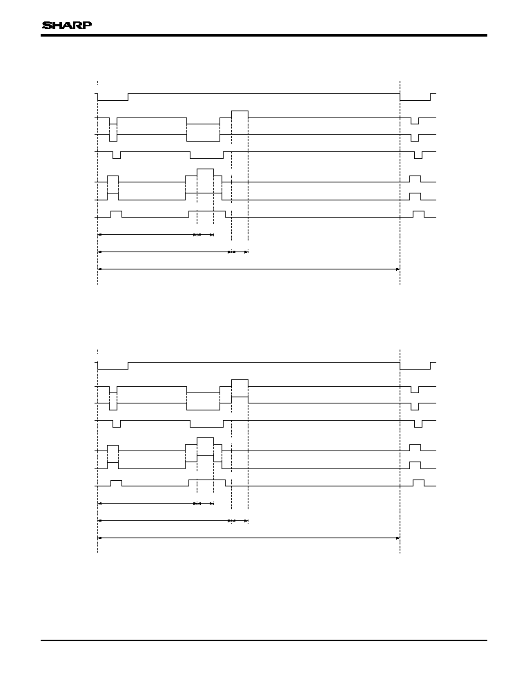
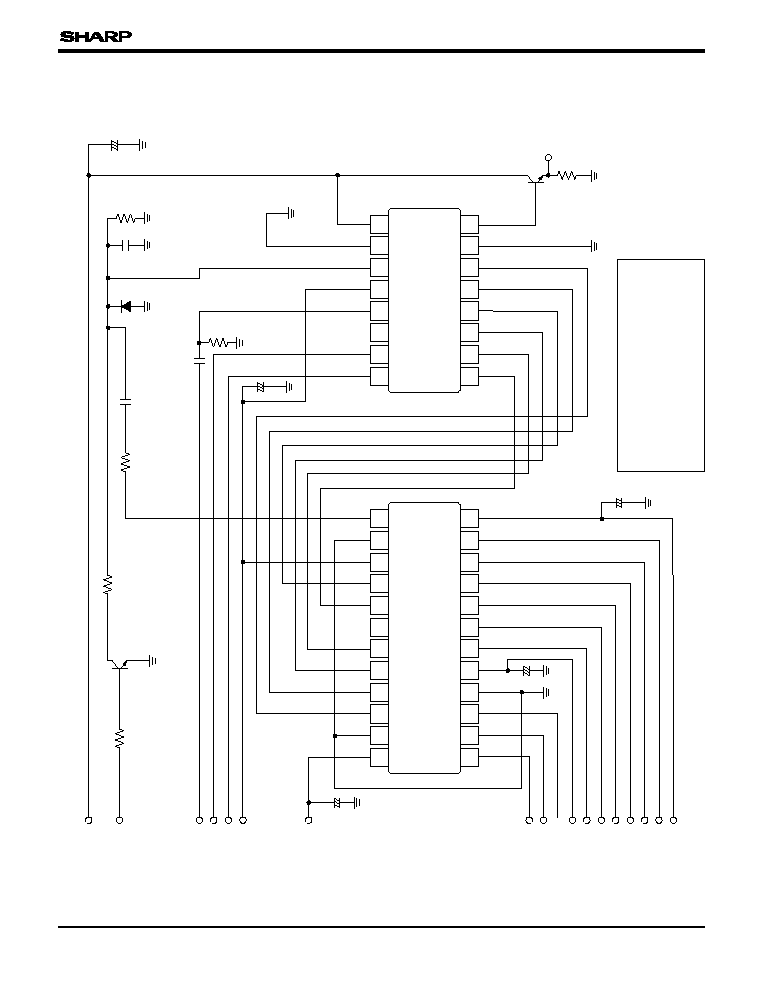
SYSTEM CONFIGURATION EXAMPLE
+
OD
PW
OFD
ÿ
V3B
ÿ
V3A
ÿ
V4
GND
NC
ÿ
H1
ÿ
H2
OS
GND
ÿ
V1A
ÿ
V1B
ÿ
V2
ÿ
RS
V
3B
V
3A
V
1B
V
1A
V
Ma
V
H
V
4
V
2
V
L
V
Mb
POFD
NC
V
H
ÿ
H2
VH
1BX
V
3X
V
2X
VH
3BX
V
4X
V
OFDH
V
1X
VH
3AX
VH
1AX
+3.3 V
OFDX
ÿ
H1
ÿ
RS
V
L
(V
PW
)
CCD
OUT
V
OFDH
VH
3BX
OFDX
V
2X
V
1X
V
3X
V
DD
GND
V
4X
VH
3AX
VH
1BX
VH
1AX
+
+
1
2
3
4
5
6
7
8
12
24
23
22
21
20
19
18
17
13
11
14
10
15
9
16
2
3
4
5
6
7
8
15
14
1
16
13
12
11
10
9
LR36685
LZ23H3V1
(*1)
(*1)
V
OD
OFDC
270
pF
100 $
1 M$
1 M$
5.6 k$
18 k$
0. 47 µF
0. 01 µF
+
+
(*1) ÿ
RS
, OFD :
Use the circuit parameter indicated in
this circuit example, and do not connect
to DC voltage directly.
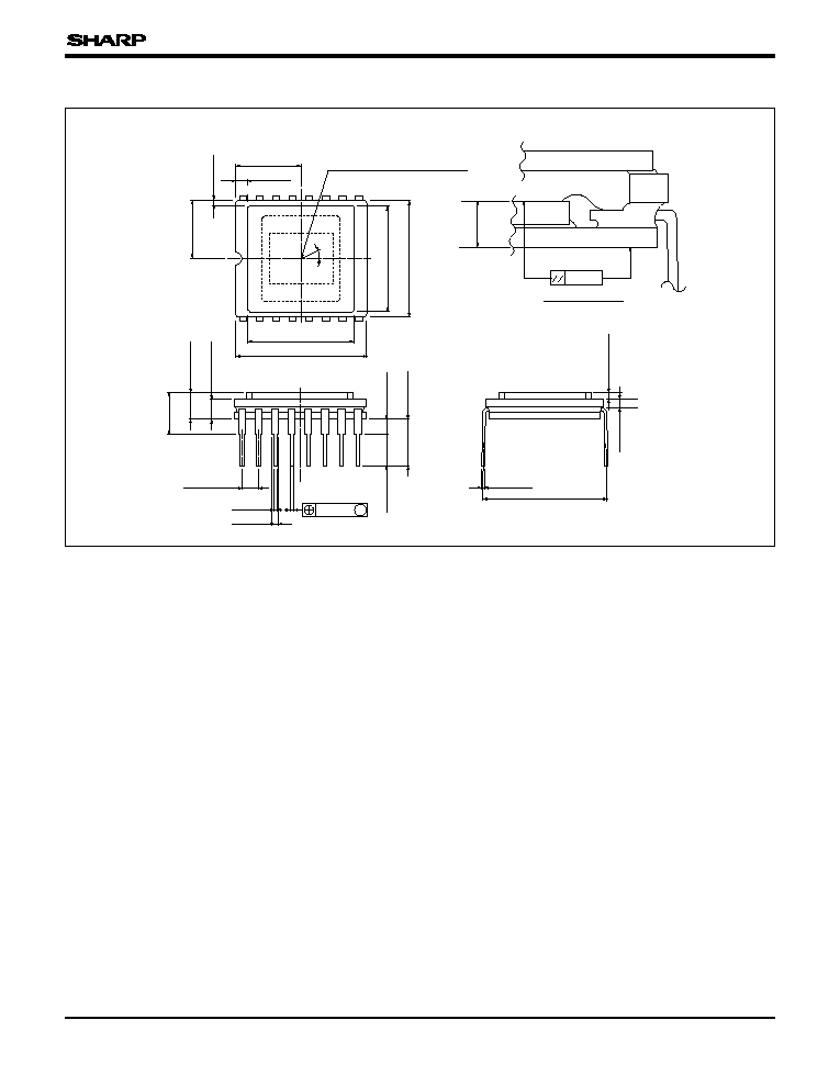
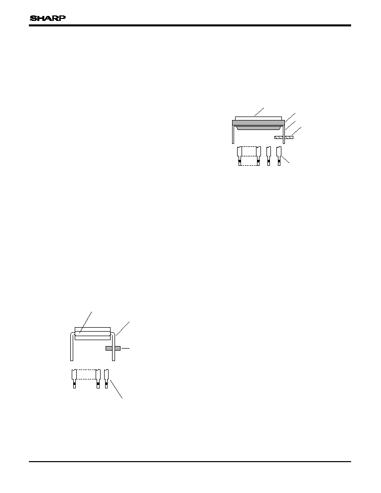
PACKAGES FOR CCD AND CMOS DEVICES
18
PACKAGE
(Unit : mm)
0.04
1.66
±0.10
Package (Cerdip)
Glass Lid
CCD
Cross Section A-A'
1
8
14.00
±0.15
16
9
11.20
±0.10
()
12.40
±0.15
6.20
±0.15
0.60
±0.60
7.00
±0.15
1.40
±0.60
CCD
( : Lid's size)
11.20
±0.10
()
Center of effective imaging area
and center of package
0.25
±0.10
12.70
±0.25
0.80
±0.05
()
1.05
MIN.
0.46
TYP.
0.90
TYP.
2.63
TYP.
5.24
MAX.
3.42
±0.25
1.27
±0.25
3.90
±0.30
2.60
±0.20
P-1.78
TYP.
A'
A
Rotation error of die : ¨ = 1.5∞
MAX.
M
0.25
16 WDIP (WDIP016-N-0500C)
PRECAUTIONS FOR CCD AREA SENSORS
1. Package Breakage
In order to prevent the package from being broken,
observe the following instructions :
1) The CCD is a precise optical component and
the package material is ceramic or plastic.
Therefore,
¯ Take care not to drop the device when
mounting, handling, or transporting.
¯ Avoid giving a shock to the package.
Especially when leads are fixed to the socket
or the circuit board, small shock could break
the package more easily than when the
package isn't fixed.
2) When applying force for mounting the device or
any other purposes, fix the leads between a
joint and a stand-off, so that no stress will be
given to the jointed part of the lead. In addition,
when applying force, do it at a point below the
stand-off part.
(In the case of ceramic packages)
≠ The leads of the package are fixed with low
melting point glass, so stress added to a
lead could cause a crack in the low melting
point glass in the jointed part of the lead.
(In the case of plastic packages)
≠ The leads of the package are fixed with
package body (plastic), so stress added to a
lead could cause a crack in the package
body (plastic) in the jointed part of the lead.
3) When mounting the package on the housing,
be sure that the package is not bent.
≠ If a bent package is forced into place
between a hard plate or the like, the pack-
age may be broken.
4) If any damage or breakage occurs on the sur-
face of the glass cap, its characteristics could
deteriorate.
Therefore,
¯ Do not hit the glass cap.
¯ Do not give a shock large enough to cause
distortion.
¯
Do not scrub or scratch the glass surface.
≠ Even a soft cloth or applicator, if dry, could
cause dust to scratch the glass.
2. Electrostatic Damage
As compared with general MOS-LSI, CCD has
lower ESD. Therefore, take the following anti-static
measures when handling the CCD :
1) Always discharge static electricity by grounding
the human body and the instrument to be used.
To ground the human body, provide resistance
of about 1 M$ between the human body and
the ground to be on the safe side.
2) When directly handling the device with the
fingers, hold the part without leads and do not
touch any lead.
Glass cap
Package
Lead
Fixed
Stand-off
Fixed
Lead
Stand-off
Low melting point glass
19
PRECAUTIONS FOR CCD AREA SENSORS

3) To avoid generating static electricity,
a. do not scrub the glass surface with cloth or
plastic.
b. do not attach any tape or labels.
c. do not clean the glass surface with dust-
cleaning tape.
4) When storing or transporting the device, put it in
a container of conductive material.
3. Dust and Contamination
Dust or contamination on the glass surface could
deteriorate the output characteristics or cause a
scar. In order to minimize dust or contamination on
the glass surface, take the following precautions :
1) Handle the CCD in a clean environment such
as a cleaned booth. (The cleanliness level
should be, if possible, class 1 000 at least.)
2) Do not touch the glass surface with the fingers.
If dust or contamination gets on the glass
surface, the following cleaning method is
recommended :
¯ Dust from static electricity should be blown
off with an ionized air blower. For anti-
electrostatic measures, however, ground all
the leads on the device before blowing off
the dust.
¯
The contamination on the glass surface
should be wiped off with a clean applicator
soaked in Isopropyl alcohol. Wipe slowly and
gently in one direction only.
≠ Frequently replace the applicator and do not
use the same applicator to clean more than
one device.
Note : In most cases, dust and contamination
are unavoidable, even before the device
is first used. It is, therefore, recommended
that the above procedures should be
taken to wipe out dust and contamination
before using the device.
4. Other
1) Soldering should be manually performed within
5 seconds at 350 ∞C maximum at soldering iron.
2) Avoid using or storing the CCD at high tem-
perature or high humidity as it is a precise
optical component. Do not give a mechanical
shock to the CCD.
3) Do not expose the device to strong light. For
the color device, long exposure to strong light
will fade the color of the color filters.
20
PRECAUTIONS FOR CCD AREA SENSORS