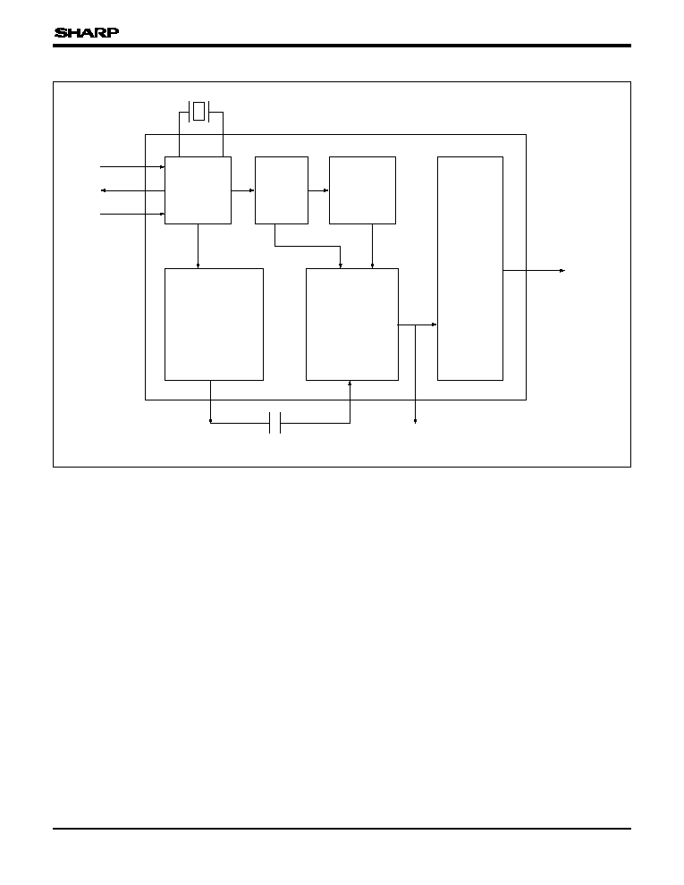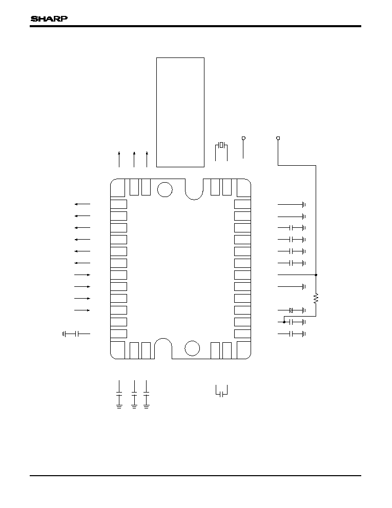
PACKAGES FOR CCD AND CMOS DEVICES
12
0.04
0.04
,,,,,,,,,,,,,,,,,,,,,,,,,,,,,,,,,,,,,,,,,,,,,,,,,,,,,,,,,,,,,,,,,,,,,,,,,
,,,,,,,,,,,,,,,,,,,,,,,,,,,,,,,,,,,,,,,,,,,,,,,,,,,,,,,,,,,,,,,,,,,,,,,,,
,,,,,,,,,,,,,,,,,,,,,,,,,,,,,,,,,,,,,,,,,,,,,,,,,,,,,,,,,,,,,,,,,,,,,,,,,
,,,,,,,,,,,,,,,,,,,,,,,,,,,,,,,,,,,,,,,,,,,,,,,,,,,,,,,,,,,,,,,,,,,,,,,,,
,,,,,,,,,,,,,,,,,,,,,,,,,,,,,,,,,,,,,,,,,,,,,,,,,,,,,,,,,,,,,,,,,,,,,,,,,
,,,,,,,,,,,,,,,,,,,,,,,,,,,,,,,,,,,,,,,,,,,,,,,,,,,,,,,,,,,,,,,,,,,,,,,,,
,,,,,,,,,,,,,,,,,,,,,,,,,,,,,,,,,,,,,,,,,,,,,,,,,,,,,,,,,,,,,,,,,,,,,,,,,
,,,,,,,,,,,,,,,,,,,,,,,,,,,,,,,,,,,,,,,,,,,,,,,,,,,,,,,,,,,,,,,,,,,,,,,,,
,,,,,,,,,,,,,,,,,,,,,,,,,,,,,,,,,,,,,,,,,,,,,,,,,,,,,,,,,,,,,,,,,,,,,,,,,
,,,,,,,,,,,,,,,,,,,,,,,,,,,,,,,,,,,,,,,,,,,,,,,,,,,,,,,,,,,,,,,,,,,,,,,,,
,,,,,,,,,,,,,,,,,,,,,,,,,,,,,,,,,,,,,,,,,,,,,,,,,,,,,,,,,,,,,,,,,,,,,,,,,
,,,,,,,,,,,,
,,,,,,,,,,,,
,,,,,,,,,,,,
,,,,,,,,,,,,
,,,,,,,,,,,,
,,,,,,,,,,,,
,,,,,,,,,,,,
,,,,
,,,,
,,,,
,,,,
,,,,
,,,,
,,,,
,,,,
,,,,
,,,,
,,,,
,,,,
,,,,
,,,,
,,,,
,,,,
,,,,
,,,,
,,,,,,,
,,,,,,,
,,,,,,,
,,,,,,,
,,,,,,,
,,,,,,,
,,,,,,,
,,,,,,,
,,,,,,,
,,,,,,,
,,,,,,,
,,,,,,,
,,,,,,,
,,,,,,,
,,,,,,,
,,,,,,,
,,,,,,,
,,,,,,,
,,,,,,,
,,,,,,,
,,,,,,,
,,,,,,,
,,,,,,,
,,,,,,,
,,,,,,,
,,,,,,,
,,,,,,,
,,,,,,,
,,,,,,,
,,,,,,,
,,,,,,,
,,,,,,,
,,,,,,,
,,,,,,,
,,,,,,,
,,,,,,,
,,,,,,,,,,,,,,,,,,,,,,,,,
,,,,,,,,,,,,,,,,,,,,,,,,,
,,,,,,,,,,,,,,,,,,,,,,,,,
,,,,,,,,,,,,,,,,,,,,,,,,,
,,,,,,,,,,,,,,,,,,,,,,,,,
,,,,,,,,,,,,,,,,,,,,,,,,,
,,,,
,,,,
,,,,
,,,,
,,,,
,,,,
,,,,
,,,,
,,,,
,,,,
,,,,
,,,,
,,,,
,,,,
,,,,
,,,,
,,,,
,,,,,,,
,,,,,,,
,,,,,,,
,,,,,,,
,,,,,,,
,,,,,,,
,,,,,,,
,,,,,,,
,,,,,,,
,,,,,,,
,,,,,,,
,,,,,,,
,,,,,,,
,,,,,,,
,,,,,,,
,,,,,,,
,,,,,,,
,,,,,
,,,,,
,,,,,
,,,,,
,,,,,
,,,,,
,,,,,
,,,,,
,,,,,
,,,,,
,,,,,
,,,,,
,,,,,
,,,,,
,,,,,
,,,,,
,,,,,
,,,,,,
,,,,,,
,,,,,,
,,,,,,
,,,,,,
,,,,,,
,,,,,,
,,,,,,
,,,,,,
,,,,,,
,,,,,,
,,,,,,
,,,,,,
,,,,,,
,,,,,,
,,,,,,
,,,,,,
,,,,,,,
,,,,,,,
,,,,,,,
,,,,,,,
,,,,,,,
,,,,,,,
,,,,,,,
,,,,,,,
,,,,,,,
,,,,,,,
,,,,,,,
,,,,,,,
,,,,,,,
,,,,,,,
,,,,,,,
,,,,,,,
,,,,,,,
,,,,,,,
,,,,,,,
,,,,,,,
,,,,,,,
,,,,,,,
,,,,,,,
,,,,,,,
,,,,,,,
,,,,,,,
,,,,,,,
,,,,,,,
,,,,,,,
,,,,,,,
,,,,,,,
,,,,,,,
,,,,,,,
,,,,,,,
,,,,,,,
,,,,,,,
,,,,,,,
,,,,,,,
,,,,,,,
,,,,,,,
,,,,,,,
,,,,,,,
,,,,,,,
,,,,,,,
,,,,,,,
,,,,,,,
,,,,,,,
,,,,,,,
,,,,,,,
,,,,,,,
,,,,,,,
,,,,,,,
,,,,,,,
,,,,,,,
,,,,,,,
,,,,,,,
,,,,,,,
,,,,,,,
,,,,,,,
,,,,,,,
,,,,,,,
,,,,,,,
,,,,,,,
,,,,,,,
,,,,,,,
,,,,,,,
,,,,,,,
,,,,,,,
,,,,,,,
,,,,,,,
,,,,,,,
,,,,,,,
,,,,,,,
,,,,,,,
,,,,,,,
,,,,,,,
,,,,,,,
,,,,,,,
,,,,,,,
,,,,,,,
,,,,,,,
,,,,,,,
,,,,,,,
,,,,,,,
,,,,,,,
,,,,,,,
,,,,,,,
,,,,,,,
,,,,,,,
,,,,,,,
,,,,,,,
,,,,,,,
,,,,,,,
,,,,,,,
,,,,,,,
,,,,,,,
,,,,,,,
,,,,,,,
,,,,,,,
,,,,,,,
,,,,,,,
,,,,,,,
,,,,,,
,,,,,,
,,,,,,
,,,,,,
,,,,,,
,,,,,,
,,,,,,
,,,,,,
,,,,,,
,,,,,,
,,,,,,
,,,,,,
,,,,,,
,,,,,,
,,,,,,
,,,,,,
,,,,,,
,,,,,,,
,,,,,,,
,,,,,,,
,,,,,,,
,,,,,,,
,,,,,,,
,,,,,,,
,,,,,,,
,,,,,,,
,,,,,,,
,,,,,,,
,,,,,,,
,,,,,,,
,,,,,,,
,,,,,,,
,,,,,,,
,,,,,,,
,,,,,,
,,,,,,
,,,,,,
,,,,,,
,,,,,,
,,,,,,
,,,,,,
,,,,,,
,,,,,,
,,,,,,
,,,,,,
,,,,,,
,,,,,,
,,,,,,
,,,,,,
,,,,,,
,,,,,,
,,,,,,,
,,,,,,,
,,,,,,,
,,,,,,,
,,,,,,,
,,,,,,,
,,,,,,,
,,,,,,,
,,,,,,,
,,,,,,,
,,,,,,,
,,,,,,,
,,,,,,,
,,,,,,,
,,,,,,,
,,,,,,,
,,,,,,,
,,,,,,
,,,,,,
,,,,,,
,,,,,,
,,,,,,
,,,,,,
,,,,,,
,,,,,,
,,,,,,
,,,,,,
,,,,,,
,,,,,,
,,,,,,
,,,,,,
,,,,,,
,,,,,,
,,,,,,
,,,,,,,
,,,,,,,
,,,,,,,
,,,,,,,
,,,,,,,
,,,,,,,
,,,,,,,
,,,,,,,
,,,,,,,
,,,,,,,
,,,,,,,
,,,,,,,
,,,,,,,
,,,,,,,
,,,,,,,
,,,,,,,
,,,,,,,
,,,,,,
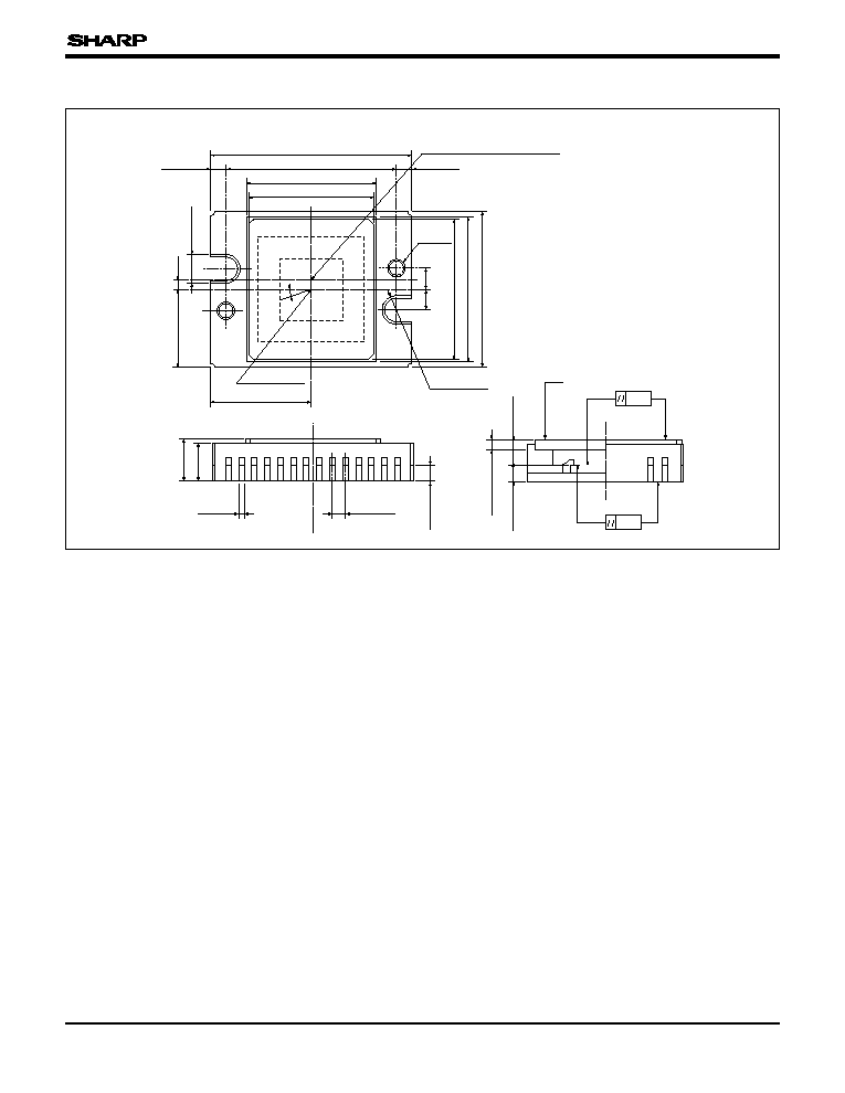
15.60
±0.10
13.30
±0.10
1.15
±0.10
1.15
±0.10
10.80
±0.05
(2)
1.60
1.60
11.00
±0.10
12.00
±0.10
2-ÿ1.30
±0.20
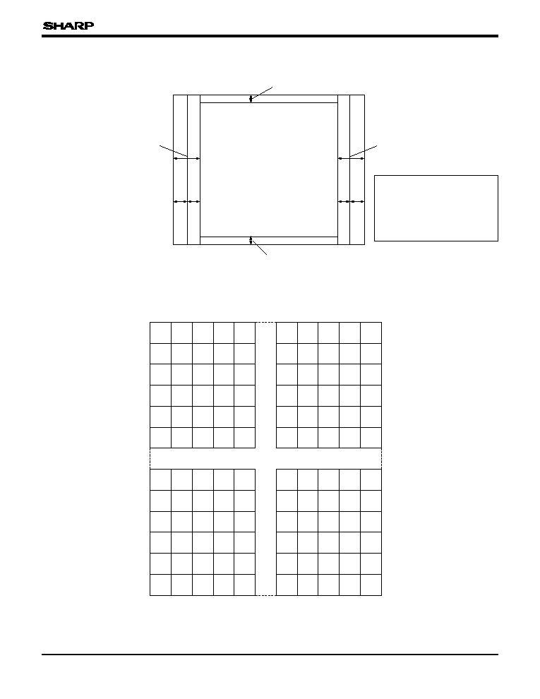
Center of effective imaging area
10.00
±0.10
9.80
±0.05
(2)
2-R1.05
±0.20
Center of die
7.80
±0.075
6.00
±0.075
0.65
2.10
±0.20
¨
CMOS
Rotation error of die : ¨ = 1.0∞
MAX.
( 1 : Effective imaging area)
( 2 : Lid's size)
Refractive index : nd = 1.5
(1)
(1)
1.26
±0.10
1.86
±0.10
0.70
±0.05
(2)
1.20
±0.12
A
A'
Glass Lid
Package
CMOS
A
A'
0.40
TYP.
P-1.00
TYP.
2.90
±0.10
3.12
±0.20
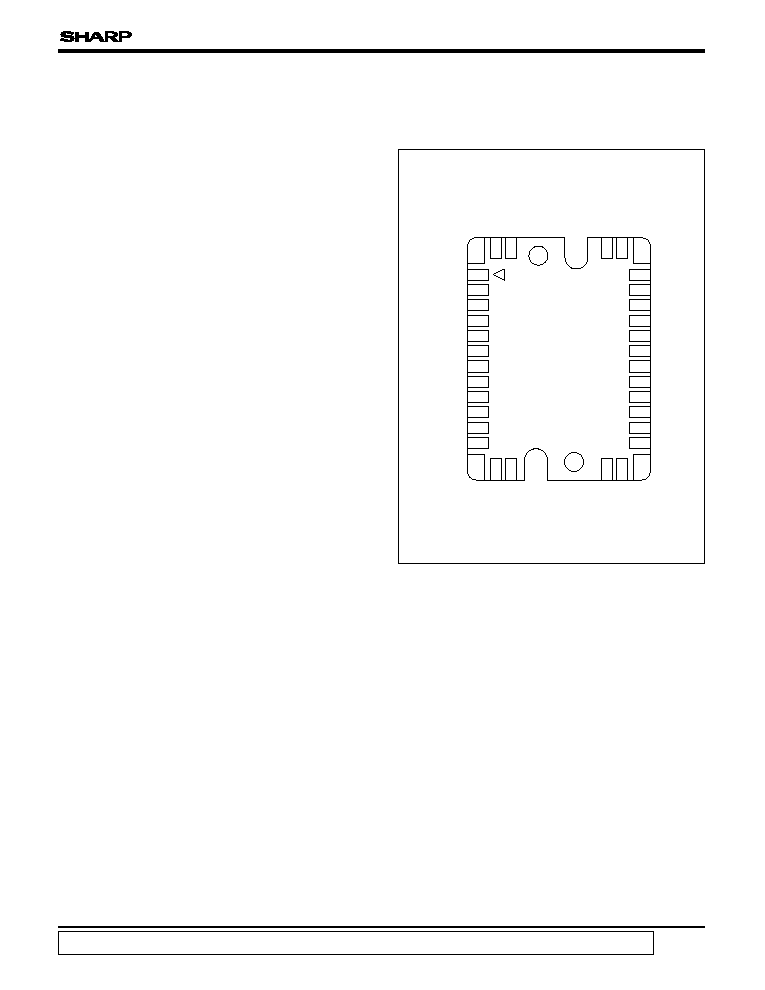
36 WLCC (WLCC036-N-R625)
PACKAGE
(Unit : mm)