 | –≠–ª–µ–∫—Ç—Ä–æ–Ω–Ω—ã–π –∫–æ–º–ø–æ–Ω–µ–Ω—Ç: PC814 | –°–∫–∞—á–∞—Ç—å:  PDF PDF  ZIP ZIP |
PC814 Series
PC814 Series
AC Input Photocoupler
s
Features
s
Applications
2. High isolation voltage between input and
3. Compact dual-in-line package
4. Current transfer ratio
1. Programmable controllers
2. Telephone sets, telephone exchangers
3. System appliances
4. Signal transmission between circuits of
CTR : MIN. 20% at I
F
= ± 1mA, V
CE
= 5V
different potentials and impedances
s
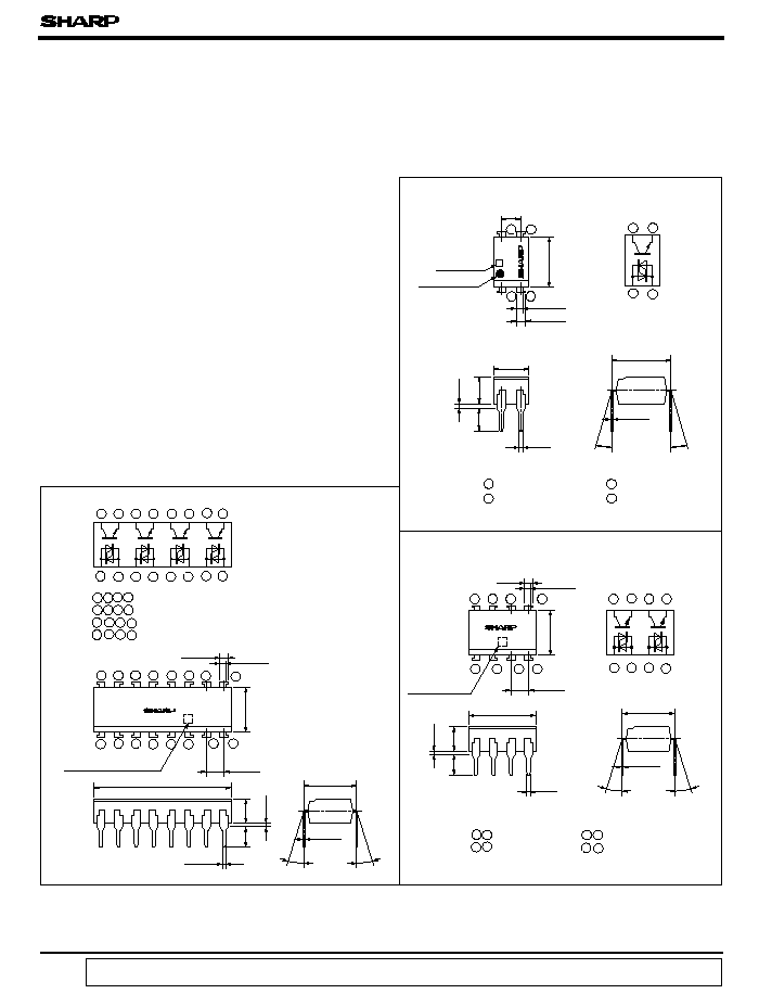
Outline Dimensions
( Unit : mm)
data books, etc. Contact SHARP in order to obtain the latest version of the device specification sheets before using any SHARP's device.
"
"
In the absence of confirmation by device specification sheets, SHARP takes no responsibility for any defects that occur in equipment using any of SHARP's devices, shown in catalogs,
5. Recognized by UL, file No. E64380
PC844
PC844
PC814
Internal connection
PC814
diagram
CTR rank mark
rank mark
PC824
PC824
Internal connection diagram
CTR
2
1
4
3
1 Anode, Cathode
2 Anode, Cathode
3 Emitter
4 Collector
4
1
2
3
1
2
3
4
5
6
7
8
1
2
3
4
5
6
7
8
5 7 Emitter
6 8 Collector
1 3 Anode,Cathode
2 4 Anode,Cathode
1
2
3
4
5
6
7
8
9
CTR
rank mark
Internal connection diagram
1
2
3
4
5
6
7
8
9
1 3 5 7 Anode, Cathode
2 4 6 8 Anode, Cathode
9
Emitter
Collector
PC814
( 1-channel type )
PC824
(2-channel type )
PC844
( 4-channel type )
1. AC input
Primary side mark
g Lead forming type ( I type ) and taping reel type ( P type ) are also available. (
PC814I/PC814P
)
output ( V : 5 000V
rms
)
6.5
±
0.5
0.9
±
0.2
1.2
±
0.3
2.54
±
0.25
19.82
±
0.5
3.5
±
0.5
3.0
±
0.5
0.5
±
0.1
7.62
±
0.3
0.26
±
0.1
=
0 to 13
∞
0.5
TYP.
6.5
±
0.5
1.2
±
0.3
0.9
±
0.2
2.54
±
0.25
=
0 to 13
∞
9.66
±
0.5
3.5
±
0.5
3.0
±
0.5
0.5
TYP.
0.5
±
0.1
0.26
±
0.1
7.62
±
0.3
6.5
±
0.5
2.54
±
0.25
0.9
±
0.2
1.2
±
0.3
4.58
±
0.5
3.5
±
0.5
3.0
±
0.5
0.5
±
0.1
0.5
TYP.
7.62
±
0.3
0.26
±
0.1
=
0 to 13
∞
11
12
13
14
15
16
11
12
13
14
15
16
11
12
13
14
15
16
10
10
10
PC814 Series
*3 For 10 seconds
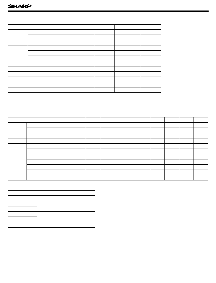
*4 Classification table of current transfer ratio
Parameter
Symbol
Conditions
Forward voltage
V
F
I
F
= ± 20mA
Peak forward voltage
V
FM
I
FM
= ± 0.5V
Terminal capacitance
C
t
V = 0, f = 1kHz
Collector dark current
I
CEO
V
CE
= 20V, I
F
= 0
Transfer
charac-
teristics
*4
Current transfer ratio
CTR
I
F
= ± 1mA, V
CE
= 5V
Collector-emitter saturation voltage
V
CE( sat )
I
F
= ± 20mA, I
C
= 1mA
Isolation resistance
R
ISO
Floating capacitance
V = 0, f = 1MHz
Cut-off frequency
f
c
t
r
V
CE
= 2V, I
C
= 2mA, R
L
=
100
t
f
MIN.
TYP.
MAX.
Unit
-
1.2
1.4
V
-
-
3.0
V
-
50
250
pF
-
-
10
- 7
A
20
-
300
%
-
0.1
0.2
V
5 x 10
10
10
11
-
0.6
1.0
pF
15
80
-
kHz
-
-
4
18
µ
s
-
3
18
µ
s
( Ta = 25∞C)
s
Absolute Maximum Ratings
( Ta = 25∞C)
C
f
V
CE
= 5V, I
C
= 2mA, R
L
= 100
, - 3dB
Parameter
Symbol
Rating
Unit
Input
Forward current
I
F
± 50
mA
*1
Peak forward current
I
FM
± 1
A
Power dissipation
P
70
mW
Output
Collector-emitter voltage
V
CEO
35
V
Emitter-collector voltage
V
ECO
6
V
Collector current
I
C
50
mA
Collector power dissipation
P
C
150
mW
Total power dissipation
P
tot
200
mW
*2
Isolation voltage
V
iso
Operating temperature
T
opr
- 30 to + 100
∞C
Storage temperature
T
stg
- 55 to + 125
∞C
*3
Soldering temperature
T
sol
260
∞C
*1 Pulse width <=100
µ
s, Duty ratio : 0.001
s
Electro-optical Characteristics
Model No.
Rank mark
PC814A
A
50 to 150
PC824A
PC844A
PC814
A or no mark
20 to 300
PC824
PC844
Response time
Rise time
Fall time
Input
Output
CTR ( % )
5 000
*2 40 to 60% RH, AC for 1 minute
DC500V, 40 to 60% RH
V
rms
Duty ratio
5
5
10
20
100
50
200
500
2
10
- 3
10
- 2
5
2
10
- 1
5
2
5
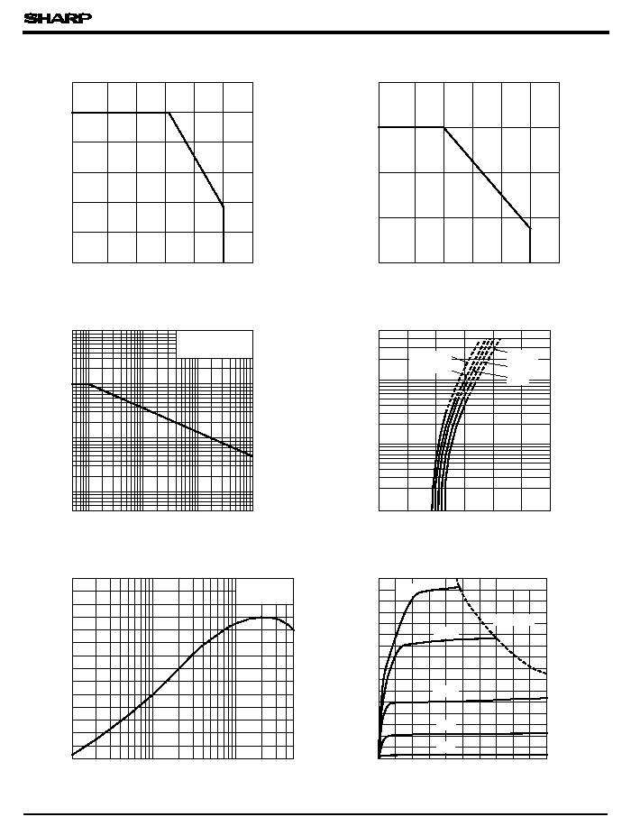
Fig. 3 Peak Forward Current vs. Duty Ratio
0.1
0.5
0.2
1
2
5
10
0
20
50
60
80
100
120
140
20
40
0
0
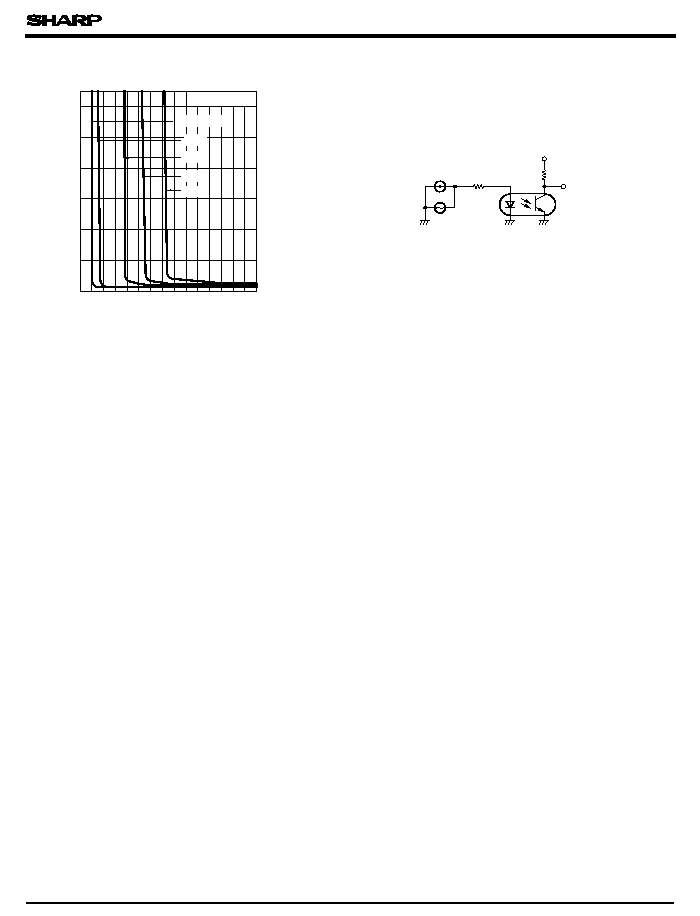
Collector-emitter voltage V
CE
(V)
10
2
20
30
4
6
8
10
20mA
10mA
5mA
1mA
Fig. 6 Collector Current vs.
Collector-emitter Voltage
Peak forward current I
FM
(
mA
)
Forward current I
F
( mA )
0
- 30
10
F
(
mA
)
0
25
50
75
100
125
20
30
40
50
60
Ambient temperature T
a
(∞C)
PC814 Series
25∞C
0∞C
0
1
2
F
(
mA
)
0.5
1.0
1.5
2.0
2.5
3.0
5
10
20
50
100
200
500
50∞C
Fig. 4 Forward Current vs. Forward Voltage
- 25∞C
Forward voltage V
F
(V)
0
0
125
100
200
50
150
25
50
75
100
Ambient Temperature
C
(
mW
)
- 30
Fig. 2 Collector Power Dissipation vs.
a
(∞C)
Fig. 1 Forward Current vs. Ambient
Temperature
Pulse width <=100
µ
s
Fig. 5 Current Transfer Ratio vs. Forward
Current
Forward current I
Ambient temperature T
Collector power dissipation P
Forward current I
1
Current transfer ratio CTR
(
%
)
Collector current I
C
(mA
)
T
a
= 25∞C
V
CE
= 5V
T
a
= 25∞C
T
a
= 25∞C
P
C
(MAX. )
I
F
= 30mA
T
a
= 75∞C
10 000
5 000
2 000
1 000
50
0
100
150
0
25
100
75
50
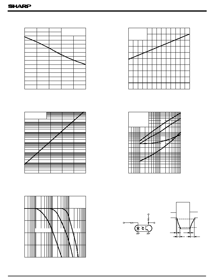
Relative current transfer ratio
(
%
)
Fig. 7 Relative Current Transfer Ratio vs.
Ambient Temperature
25
0
50
75
100
Fig. 9 Collector Dark Current vs.
Ambient Temperature
Fig.11 Frequency Response
Frequency f ( kHz )
0.2
20
2
200
1 000
0
100
1k
0.5 1
5
10
50 100
500
Fig. 8 Collector-emitter Saturation Voltage
vs. Ambient Temperature
Ambient temperature T
a
(∞C)
Ambient temperature T
a
(∞C)
Collector emitter saturation voltage V
CE
( sat
)
(
V
)
Collector dark current I
CEO
(
A
)
Ambient temperature T
a
(∞C)
Voltage gain A
v
(
dB
)
L
( k
)
100
5
2
1
Response time
(
µ
s
)
0.5
0.1
0.2
0.03
0.1
1
10
0.2
0.5
2
5
50
20
10
PC814 Series
Test Circuit for Response Time
V
CC
t
t
r
t
s
90
%
10
%
t
d
Output
Input
R
L
Input
Output
R
D
- 30
- 20
- 15
- 10
- 5
f
0
- 30
0.01
0
20
40
60
80
100
0.02
0.03
0.04
0.05
0.06
0.07
0.08
0.09
0.1
I
F
= 1mA
V
CE
= 5V
V
CE
= 20V
V
CE
= 5V
I
C
= 2mA
T
a
= 25∞C
R
L
= 10k
t
r
t
f
t
d
t
s
V
CE
= 2V
I
C
= 2mA
T
a
= 25∞C
I
F
= 20mA
I
C
= 1mA
- 30
10
- 12
10
- 11
10
- 10
10
- 9
10
- 8
10
- 7
10
- 6
Fig.10 Response Time vs. Load Resistance
Load resistance R
Collector-emitter saturation voltage V
CE
( sat
)
(
V
)
Forward current I
F
( mA )
0
0
2
4
6
2
4
6
8
10
1mA
3mA
5
3
1
9
7
5
3
1
5mA
7mA
11 12 13 14 15
Fig.12 Collector-emitter Saturation Voltage
vs. Forward Current
PC814 Series
V
CC
R
L
Output
R
D
Test Circuit for Frepuency Response
T
a
= 25∞C
I
C
= 0.5mA
Please refer to the chapter " Precautions for Use "
q