S102S01/S102S02/S202S01/S202S02
S102S01/S102S02
S202S01/S202S02
s
Applications
s
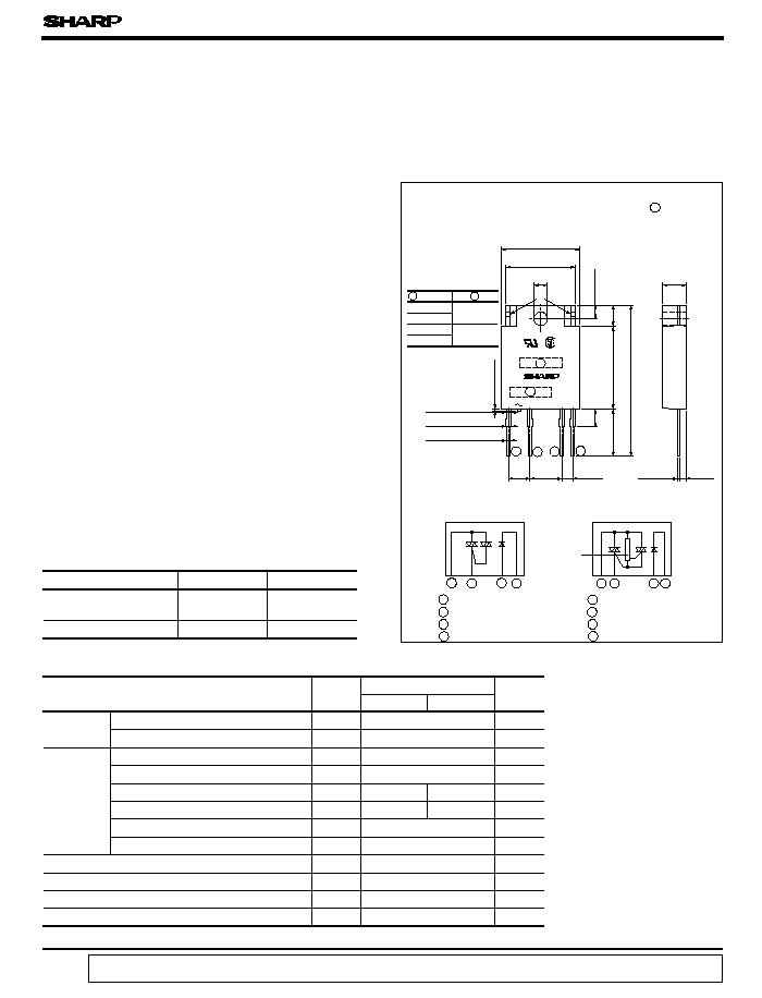
Outline Dimensions
( Unit : mm)
s
Absolute Maximum Ratings
(Ta = 25∞C)
SIP Type SSR for Medium
Power Control
Parameter
Symbol
Rating
Unit
S102S01
S102S02
S202S01
S202S02
Input
Forward current
I
F
50
mA
Reverse voltage
V
R
6
V
Output
*1
RMS ON-state current
I
T
8
*2
Peak one cycle surge current
I
surge
80
A
Repetitive peak OFF-state voltage
V
DRM
400
600
V
V
DSM
400
600
V
Critical rate of rise of ON-state
dI/dt
50
A/
µ
s
Operating frequency
f
45 to 65
Hz
*3
Isolation voltage
V
iso
Operating temperature
T
opr
- 25 to + 100
∞C
Storage temperature
T
stg
- 30 to + 125
∞C
*4
Soldering temperature
T
sol
260
∞C
( 36.0
)
(5.08) (7.62)
(2.54)
(1.4)
+
Internal connection diagram
*
A
B
1
2
3
4
Zero-Cross
Circuit
1 2
3 4
1
2
3 4
3 Input (
+
)
3 Input (
+
)
A (Model No.)
B
S102S01
8A125VAC
S102S02
S202S01
8A250VAC
S202S02
data books, etc. Contact SHARP in order to obtain the latest version of the device specification sheets before using any SHARP's device.
"
"
In the absence of confirmation by device specification sheets, SHARP takes no responsibility for any defects that occur in equipment using any of SHARP's devices, shown in catalogs,
are common to terminal 1 .
g
Do not allow external connection.
( )
:
Typical dimensions
s
Features
Non-repetitive peak OFF-state voltage
current
2 Output (Triac T1 )
1 Output (Triac T2 )
1 Output (Triac T2 )
2 Output (Triac T1 )
2. RMS ON-state current
I
T
: 8 Arms at T
C
<= 80∞C
( With heat sink )
3. Built-in zero-cross circuit
(S102S02/S202S02 )
4. High repetitive peak OFF-state voltage
S102S01/S102S02
V
DRM
: MIN. 400V
S202S01/S202S02
V
DRM
: MIN. 600V
5. Isolation voltage between input and output
( V
iso
1. Automatic vending machines, programmable
controllers
2. Amusement equipment
-
4 Input (
-
)
4 Input (
-
)
*1 T
C
<= 80∞C
*2 50Hz sine wave, T
j
= 25∞C
start
*3 60Hz AC for 1 minute,
shorted respectively ) .
*4 For 10 seconds
6. Approved by CSA, No. LR63705
1. High radiation resin mold package
For 100V lines
For 200V lines
For phase control
No built-in zero-cross circuit
S102S01
S202S01
Built-in zero-cross circuit
S102S02
S202S02
(Note)
When the isolation voltage
A
rms
V
rms
s
Model Line-ups
4 000
40 to 60 % RH, Apply voltages
between input and output, by
the dielectric withstand
voltage tester with zero-
cross circuit.
( Input and output shall be
insulation sheet.
Recognized by UL, file No. E94758
* The metal parts marked *
is necessary at using external
heat sink, please use the
: 4 000V
rms
)
18.5
±
0.2
16.4
±
0.3
3.2
±
0.2
3.2
±
0.2
5.5
±
0.2
5.0
±
0.3
19.6
±
0.2
g
0.2
MAX.
4
-
1.1
±
0.2
4
-
1.25
±
0.3
4
-
0.8
±
0.2
4.2
MAX.
11.2
MIN.
0.6
±
0.1
S102S01 /S202S01
S102S02 /S202S02
( Ta = 25∞C)
Parameter
Input
Forward voltage
Reverse current
Output
Holding current
Zero-cross voltage
Transfer
charac-
teristics
Isolation resistance
Turn-off time
Thermal resistance
( Between junction and case)
Thermal resistance
( Between junction and ambience)
Symbol
V
F
I
R
I
DRM
V
T
I
H
V
OX
I
FT
R
ISO
t
on
t
off
R
th(j - c)
R
th (j - a)
Conditions
I
F
= 20mA
V
R
= 3V
V
D
= V
DRM
I
F
= 20mA, I
T
= 2Arms
V
D
= 2/3 ∑ V
DRM
I
F
= 8mA
V
D
= 12V, R
L
= 30
V
D
= 6V, R
L
= 30
AC 50Hz
MIN.
TYP.
MAX.
Unit
-
1.2
1.4
V
-
-
10
-
4
A
-
-
10
-
4
A
-
-
1.5
-
-
-
50
mA
30
-
-
V/
µ
s
5
-
-
V/
µ
s
-
-
35
V
-
-
8
mA
-
-
8
mA
10
10
-
-
-
-
1
ms
-
-
10
ms
-
-
-
10
ms
-
4.5
-
∞C/W
-
-
-
40
-
∞C/W
Repetitive peak OFF-state current
ON-state voltage
Critical rate of rise of OFF-state voltage
Critical rate of rise of commutating
OFF-state voltage
T
j
= 125∞C, dI
T
/dt= - 4.0A/ms,
V
D
= 400V
Turn-on
time
S102S02
S202S02
S102S01
S202S01
S102S02
S202S02
S102S01
S202S01
S102S02
S202S02
Minimum
trigger
current
- 25
0
25
50
75
100
125
0
1
2
3
4
5
6
7
8
9
10
(1)
(2)
(3)
(4)
(5)
(6)
( 1) With infinite heat sink
( 2) With heat sink ( 200 x 200 x 2 mm Al plate )
( 3) With heat sink ( 100 x 100 x 2 mm Al plate )
( 4) With heat sink ( 75 x 75 x 2 mm Al plate )
( 5) With heat sink ( 50 x 50 x 2 mm Al plate )
( 6) Without heat sink
( Note) With the Al heat sink set up vertically,tighten
the device at the center of the Al heat sink
conductive silicone grease on the heat sink
carried out.
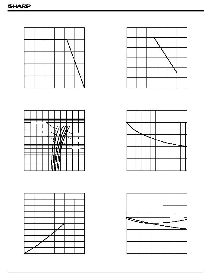
Fig. 1 RMS ON-state Current vs.
Ambient Temperature
s
Electro-optical Characteristics
Ambient temperature T
a
(∞C)
mounting plate. Forcible cooling shall not be
with a torque of 0.4N ∑ m and apply thermal
RMS ON-state current I
T
(
Arms
)
V
rms
dV/dt
DC500V, 40 to 60 % RH
( dV/dt )
C
Resistance load
S102S01/S102S02/S202S01/S202S02
S102S01/S102S02/S202S01/S202S02
Case temperature T (∞C)
- 25
0
25
50
75
100
125
0
2
4
6
8
10
Ambient temperature T
a
(∞C)
Forward current I
F
(
mA
)
- 25
0
25
50
75
100
125
0
10
20
30
40
50
60
Fig. 2 RMS ON-state Current vs.
Case Temperature
Fig. 3 Forward Current vs.
Ambient Temperature
Forward voltage V
F
(V)
Forward current I
F
(
mA
)
0
1.0
2.0
2
10
100
1
5
20
50
200
75∞C
50∞C
25∞C
0∞C
- 25∞C
Surge current I
surge
(
A
)
2
10
0
20
40
60
80
100
1
5
20
50
100
RMS ON-state current I
T
( A
rms
)
Maximum ON-state power dissipation
(W
)
0
2
4
6
8
10
12
0
2
4
6
8
10
12
14
16
18
20
Ambient temperature T
a
(∞C)
Minimum trigger current I
FT
(
mA
)
- 25
0
25
50
75
100
0
2
4
6
8
10
S102S01
S202S01
S102S02
S202S02
Fig. 7 Minimum Trigger Current vs.
Ambient Temperature (Typical Value)
Fig. 4 Forward Current vs. Forward Voltage
Fig. 6 Maximum ON-state Power Dissipation
vs. RMS ON-state Current (Typical Value)
(S102S01/S202S01 )
(S102S02/S202S02 )
Fig. 5 Surge Current vs. Power-on Cycle
Power-on cycle ( Times )
RMS ON-state current I
T
(
Arms
)
C
f= 50Hz
T
j
= 25∞C Start
T
a
= 100∞C
T
a
= 25∞C
V
D
= 12V
R
L
= 30
V
D
= 6V

S102S01/S102S02/S202S01/S202S02
- 25
0
25
50
75
100
S102S02
S202S02
S102S01
S202S01
(S102S01/S102S02 )
(S202S01/S202S02 )
Fig. 8 Repetitive Peak OFF-state Current
vs. Ambient Temperature (Typical Value)
10
- 9
10
- 8
10
- 7
10
- 6
10
- 5
10
- 4
V
D
= 400V
V
D
= 600V
Ambient temperature T
a
( ∞C )
Repetitive peak OFF-state currednt I
DRM
(
A
)
q Please refer to the chapter " Precautions for Use "