 | –≠–ª–µ–∫—Ç—Ä–æ–Ω–Ω—ã–π –∫–æ–º–ø–æ–Ω–µ–Ω—Ç: S11MA01 | –°–∫–∞—á–∞—Ç—å:  PDF PDF  ZIP ZIP |
S11MA01/S21MA01
S11MA01/S21MA01
s
Applications
s
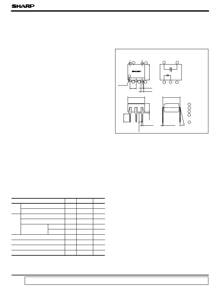
Outline Dimensions
(Unit : mm )
1. Electrical dampers for refrigerator
2. Turntable controllers for microwave oven
(Ta = 25∞C )
s
Absolute Maximum Ratings
Internal conection diagram
S11MA01
1
2
S11MA01
6
3
1
2
4
6
3
4
1 Anode
2 Cathode
3 NC
4 Anode,
Cathode
6 Anode,
Cathode
Anode
mark
data books, etc. Contact SHARP in order to obtain the latest version of the device specification sheets before using any SHARP's device.
"
"
In the absence of confirmation by device specification sheets, SHARP takes no responsibility for any defects that occur in equipment using any of SHARP's devices, shown in catalogs,
:
0 to 13
∞
Power Control
3. Ignitions circuit for oil fan heater
*1 50Hz sine wave
*3 For 10 seconds
Parameter
Symbol
Rating
Unit
Input
Forward current
I
F
50
mA
Reverse voltage
V
R
6
V
Output
RMS ON-state current
I
T
100
*1
Peak one cycle surge current
I
surge
1.2
A
Repetitive peak
OFF-state voltage
S11MA01
V
DRM
400
V
S21MA01
V
DRM
600
V
*2
Isolation voltage
V
iso
V
rms
Operating temperature
T
opr
- 25 to + 80
∞C
Storage temperature
T
stg
- 55 to + 125
∞C
*3
Soldering temperature
T
sol
260
∞C
s
Features
mA
rms
1. Low operating current type
2. Compact 5-pin dual-in-line package type
*2 AC for 1 minute, 40 to 60% RH, f = 60Hz
( MAX 60mA
rms
)
5 000
6.5
±
0.5
0.9
±
0.2
1.2
±
0.3
2.54
±
0.25
7.12
±
0.5
3.35
±
0.5
3.7
±
0.5
0.5
±
0.1
0.5
TYP.
3.5
±
0.5
7.62
±
0.3
0.26
±
0.1
3. Recognized by UL file No. E94758
6-pin DIP Type SSR for Low
S11MA01/S21MA01
s
Electro-optical Characteristics
(Ta = 25∞C )
Parameter
Input
Forward voltage
Reverse current
Output
Repetitive peak OFF-state voltage
ON-state voltage
Holding current
Critical rate of rise of OFF-state voltage
Operating current
S11MA01
S21MA01
Transfer
charac-
teristics
Mininum trigger current
Isolation resistance
Turn-on time
Symbol
V
F
I
R
I
DRM
V
T
I
H
-
I
FT
R
ISO
t
on
Conditions
I
F
= 20mA
V
R
= 3V
V
DRM
= Rated
I
T
= 0.06A
V
D
= 6V
V
D
= 6V, R
L
= 100
V
D
= 6V, R
L
= 100
, I
F
= 20mA
2
V
DRM
= ( 1/ ) ∑ Rated
MIN.
-
-
-
-
0.1
500
-
-
5 x 10
10
-
TYP.
MAX.
Unit
1.2
1.4
V
-
10
- 5
A
-
10
- 6
A
-
2.5
V
1.0
3.5
mA
-
-
V/
µ
s
-
60
-
10
mA
10
11
-
-
100
µ
s
Ambient temperature T
a
(∞C)
0
50
100
0
20
40
60
80
100
120
Ambient temperature T
a
(∞C)
Forward current I
F
(
mA
)
0
50
100
0
10
20
30
40
50
60
Ambient temperature T
a
(∞C)
0
50
100
0
20
30
40
50
60
70
Forward voltage V
F
(V)
Forward current I
F
(
mA
)
0.9
1.0
1.1
1.2
1.3
1.4
1.5
10
100
1
2
5
20
50
0∞C
- 25∞C
50∞C
25∞C
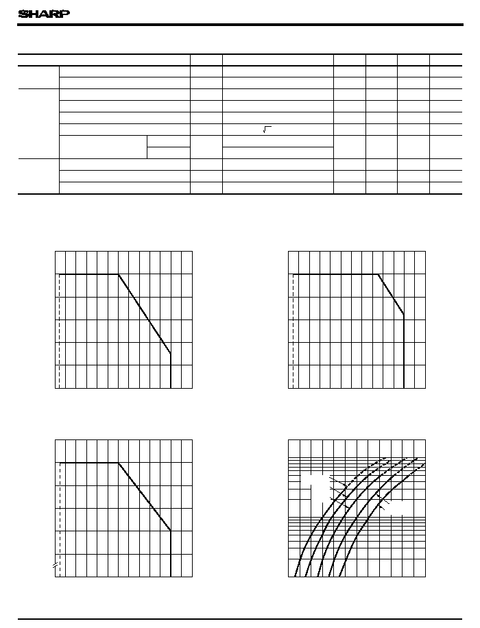
Fig. 1 RMS ON-state Current vs.
Ambient Temperature
Fig. 2 Forward Current vs.
Ambient Temperature
Fig. 3 Operating Current vs.
Ambient Temperature
Fig. 4 Forward Current vs.
Forward Voltage
RMS ON-state current I
T
(
mArms
)
mA
rms
dV/dt
- 30
- 30
T
a
= 75∞C
- 30
DC = 500V, 40 to 60% RH
Operating current
(mA
rms
)
AC100Vrms, 60Hz, Resistance load
AC200Vrms, 60Hz, Resistance load
S11MA01/S21MA01
Ambient temperature T
a
(∞C)
Minimum trigger current I
FT
(
mA
)
- 30
0
20
40
60
80
100
0
2
4
6
8
10
12
Ambient temperature T
a
(∞C)
- 30
0
20
40
60
80
100
1.0
1.1
1.2
1.3
1.4
1.5
1.6
Ambient temperature T
a
(∞C)
- 30
0
20
40
60
80
100
T
(V)
0
0.5
1.0
1.5
0
20
40
60
80
100
120
Forward current I
F
( mA )
Turn-on time t
on
(
µ
s
)
10
10
20
30
40
50
100
20
30
40
50
100
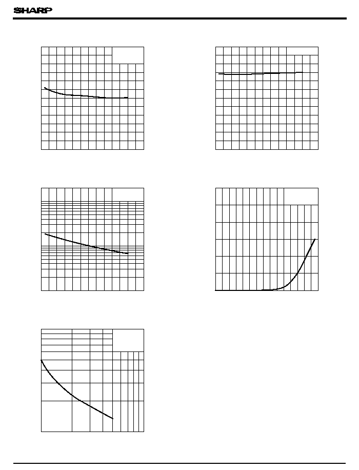
Fig. 5 Minimum Trigger Current vs.
Ambient Temperature
Fig. 6 ON-state Voltage vs.
Ambient Temperature
Fig. 7 Relative Holding Current vs.
Ambient Temperature
Fig. 8 ON-state Current vs.
ON-state Voltage
Fig. 9 Turn-on Time vs. Forward Current
Relative holding current I
H
(t∞C
)/I
H
(25∞C
)
x
100%
ON-state voltage V
T
(
V
)
ON-state current I
T
(
mA
)
ON-state voltage V
V
D
= 6V
R
L
= 100
I
T
= 0.06A
I
F
= 20mA
T
a
= 25∞C
V
D
= 6V
10
1
10
2
10
3
V
D
= 6V
R
L
= 100
I
F
= 20mA
S11MA01/S21MA01
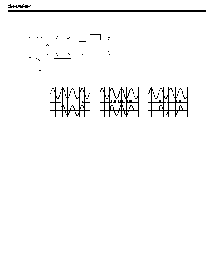
AC 100V
AC 200V
Load
Z
S
SSR
1
2
6
4
D
1
R
1
+
V
CC
(1) DC Drive
(2) Pulse Drive
AC supply voltage
Input signal
Load current
(for resistance load)
s
Basic Operation Circuit
Z
S
:
Surge absorption circuit
(3) Phase Control
and 2 to prevent reverse bias from being applied to the infrared LED.
carefully done especially for an inductive load.
be more than 10mA.
Tr1
V
I
An appropriate circuit must be chosen according to the load ( for CR, choose its constant) . This must be
2 ) Be sure to install a surge absorption circuit.
3 ) For phase control, adjust such that the load current immediately after the input signal is applied will
Notes 1) If large amount of surge is loaded onto V
CC
or the driver circuit, add a diode D
1
between terminals 1
q Please refer to the chapter " Precautions for Use"