S11MD4V/S11MD4T
S11MD4V/S11MD4T
s
Features
s
Applications
1. For triggering medium/high power triacs
1 50Hz sine wave
3 For 10 seconds
f = 60Hz
s
Absolute Maximum Ratings
( Ta = 25∞C)
s
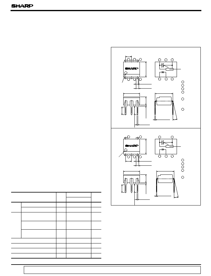
Outline Dimensions
( Unit : mm)
S11MD4V
Anode
mark
S11MD4V
S11MD4T
S11MD4T
Internal connection
diagram
Zero-cross
circuit
Internal connection
diagram
Zero-cross
circuit
Anode
mark
1
2
3
4
5
6
1
2
3
4
5
6
1
2
3
4
6
1
2
3
4
6
1 Anode
2 Cathode
3 NC
4 Anode/
Cathode
5 No exter-
nal con-
nection
6 Anode/
Cathode
1 Anode
2 Cathode
3 NC
4 Anode/
Cathode
6 Anode/
Cathode
1. Pin No. 5 completely molded for external
3. Built-in zero-cross circuit
4. High repetitive peak OFF-state voltage
(V
DRM
: MIN. 400V )
g
S11MD4V
and
S11MD4T
are for 100V
lines.
Parameter
Symbol
Rating
Unit
S11MD4V/S11MD4T
Input
Forward current
I
F
50
mA
Reverse voltage
V
R
6
V
Output
RMS ON-state
current
I
T
0.1
surge current
1
Peak one cycle
I
surge
1.2
A
Repetitive peak
OFF-state voltage
V
DRM
400
V
*2
Isolation voltage
V
iso
Operating temperature
T
opr
∞C
Storage temperature
T
stg
- 55 to +125
∞C
3
Soldering temperature
T
sol
260
∞C
Phototriac Coupler with
Built-in Zero-cross Circuit
noise resistance
(S11MD4T)
2. Dual-in-line package type
(S11MD4V)
V
iso
5. Isolation voltage between input and output
2 40 to 60% RH, AC for 1 minute,
6. Recognized by UL, file No.E64380
5 000
- 30 to +100
data books, etc. Contact SHARP in order to obtain the latest version of the device specification sheets before using any SHARP's device.
"
"
In the absence of confirmation by device specification sheets, SHARP takes no responsibility for any defects that occur in equipment using any of SHARP's devices, shown in catalogs,
: 5 000V
rms
(S11MD4V/S11MD4T )
A
rms
V
rms
:
0 to 13
∞
6.5
±
0.5
2.54
±
0.25
0.9
±
0.2
1.2
±
0.3
7.62
±
0.3
0.26
±
0.1
0.5
±
0.1
0.5
TYP.
3.5
±
0.5
3.7
±
0.5
7.12
±
0.5
3.35
±
0.5
:
0 to 13
∞
6.5
±
0.5
0.9
±
0.2
1.2
±
0.3
2.54
±
0.25
7.12
±
0.5
7.62
±
0.3
0.26
±
0.1
0.5
±
0.1
0.5
TYP.
3.5
±
0.5
3.7
±
0.5
3.35
±
0.5

S11MD4V/S11MD4T
( Ta = 25∞C)
Parameter
Symbol
Conditions MIN.
TYP.
MAX.
Unit
Forward voltage
V
F
I
F
= 20mA
-
1.2
1.4
V
Reverse current
I
R
V
R
= 3V
-
-
10
-5
A
Repetitive peak OFF-state
current
I
DRM
V
DRM
-
-
10
-6
A
ON-state voltage
V
T
I
T
= 0.1A
-
1.7
2.5
V
Holding current
I
H
V
D
= 6V
0.1
3.5
mA
Critical rate of rise of
OFF-state voltage
100
-
-
V/
µ
s
Zero-cross voltage
V
OX
-
-
35
V
Minimum trigger current
I
FT
V
D
= 6V. R
L
= 100
-
-
10
mA
Isolation resistance
R
ISO
5 x 10
10
10
11
-
Turn-on time
t
on
V
D
= 6V, R
L
= 100
, I
F
= 20mA
-
20
50
µ
s
2
V
DRM
= 1/
∑ Rated
- 30
0
20
40
60
80
100
0
0.05
0.10
Fig. 1 RMS ON-state Current vs.
Ambient Temperature
Ambient temperature T
a
(∞C)
-30
0
25
50
75
100
125
0
10
20
30
40
50
60
70
Fig. 2 Forward Current vs.
Ambient Temperature
Forward current I
F
(
mA
)
Ambient temperature T
a
(∞C)
-30
0
20
40
60
80
100
0
2
4
6
8
10
12
14
Fig. 4 Minimum Trigger Current vs.
Ambient Temperature
Minimum trigger current I
FT
(
mA
)
Ambient temperature T
a
(∞C)
T
rms
)
s
Electro-optical Characteristics
Input
Output
Transfer
charac-
teristics
1.0
RMS ON-state current I
(
A
Forward current I
F
(
mA
)
Fig. 3 Forward Current vs. Forward Voltage
Forward voltage V
F
(V)
R
L
= 100
V
D
= 6V
= Rated
dV/dt
DC500V, 40 to 60% RH
200
10
5
2
1
0
0.5
1.0
1.5
2.5
3.0
2.0
100
20
50
75∞C
50∞C
25∞C
0∞C
- 30∞C
T
a
= 100∞C
Resistance load, I
F
= 15mA

S11MD4V/S11MD4T
Ambient temperature T
a
(∞C)
-30
0
20
40
60
80
100
0.7
0.8
0.9
1.0
1.1
1.2
1.3
Fig. 5 Relative Repetitive Peak OFF-state
-30
0
20
40
60
80
100
1.4
1.5
1.6
1.7
1.8
1.9
2.0
Fig. 6 ON-state Voltage vs.
Ambient Temperature
T
(
V
)
Ambient temperature T
a
(∞C)
-30
0
20
40
60
80
100
0.2
1
0.1
0.5
2
5
10
Fig. 7 Holding Current vs.
Ambient Temperature
Holding current I
H
(
mA
)
Ambient temperature T
a
(∞C)
100
200
300
400
500
600
5
10
- 8
10
- 7
2
5
2
OFF-state voltage V
D
(V)
-30
0
20
40
60
80
100
5
2
5
2
5
2
5
10
- 6
10
- 5
10
- 7
10
- 8
10
- 9
Fig. 9 Repetitive Peak OFF-state Current vs.
Ambient temperature T
a
(∞C)
2
5
-30
0
20
40
60
80
100
15
20
25
Fig.10 Zero-cross Voltage vs.
Zero-cross voltage V
OX
(
V
)
Ambient temperature T
a
(∞C)
V
DRM
(
T
j
=T
a
)
/V
DRM
(
T
j
=
25∞C
)
DRM
(
A
)
DRM
(
A
)
R load
Voltage vs. Ambient Temperature
Relative repetitive peak OFF-state voltage
ON-state voltage V
Repetitive peak OFF-state current I
Ambient Temperature
Ambient Temperature
Repetitive peak OFF-state current I
I
T
= 100mA
V
D
= 6V
T
a
= 25∞C
V
DRM
= 400V
I
F
= 15mA
Fig. 8 Repetitive Peak OFF-state Current vs.
OFF-state Voltage
S11MD4V/S11MD4T
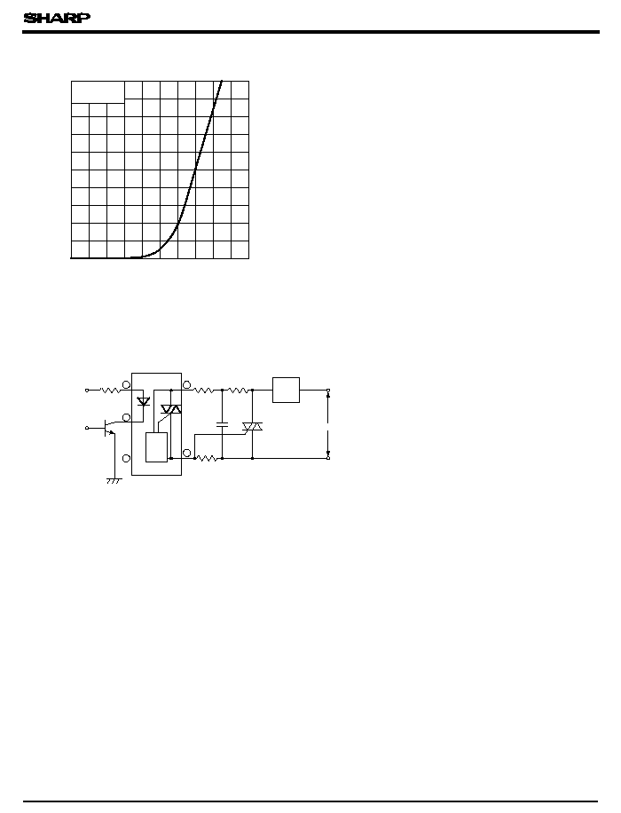
Fig.11 ON-state Current vs. ON-state Voltage
0
0.2 0.4 0.6 0.8 1.0 1.2 1.4 1.6 1.8 2.0
0
10
20
30
40
50
60
70
80
90
100
T
(
mA
)
T
(V)
Load
Zero-
cross
circuit
AC100V
1
2
3
4
6
+
V
CC
V
IN
s
Basic Operation Circuit
ON-state current I
ON-state voltage V
Medium/High Power Triac Drive Circuit
Note) Please use on condition of the triac for power triggers.
T
a
= 25∞C
I
F
= 20mA
q
Please refer to the chapter "Precautions for Use."