
S12ME1/S12ME1F
s
Features
s
Applications
3. Over voltage detection of switching power supplies
s
Outline Dimensions
( Unit : mm)
2. For triggering medium or high power thyristor and triac
S12ME1
diagram
Internal connection
S12ME1
S12ME1F
S12ME1
1
2
3
4
5
6
1
2
3
4
5
6
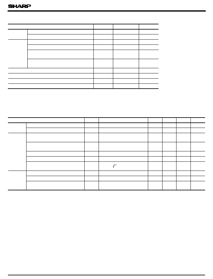
Anode
mark
1 Anode
2 Cathode
3 NC
4 Cathode
5 Anode
6 Gate
Internal connection
diagram
1
2
3
4
5
6
1
2
3
4
5
6
1 Anode
2 Cathode
3 NC
4 Cathode
5 Anode
6 Gate
Anode
mark
S12ME1/S12ME1F
Space distance : 5mm or more (
S12ME1
)
8mm or more (
S12ME1F
)
European Safety Standard Approved,
Photothyristor Coupler
1. Internal insulation distance : 0.4mm or more
2. Creepage distance : 8mm or more
3. Recognized by UL file No. E64380
g DIN-VDE0884 approved type is also available as an option.
Approved by BSI ( BS415 : NO.7088, BS7002 : NO.7410)
data books, etc. Contact SHARP in order to obtain the latest version of the device specification sheets before using any SHARP's device.
"
"
In the absence of confirmation by device specification sheets, SHARP takes no responsibility for any defects that occur in equipment using any of SHARP's devices, shown in catalogs,
Long Creepage Distance Type
g Lead forming type (I type ) and taping reel type (P type) of
S12ME1/S12ME1F
are also available. (
S12ME1I/S12ME1FI,S12ME1P/S12ME1FP
)
1. ON-OFF operation for low power load
:
0 to 13
�
6.5
�
0.5
2.54
�
0.25
1.2
�
0.3
9.22
�
0.5
7.62
�
0.3
0.26
�
0.1
0.5
�
0.1
3.7
�
0.5
3.4
�
0.3
0.5
TYP.
3.5
�
0.5
6.5
�
0.5
2.54
�
0.25
1.2
�
0.3
9.22
�
0.5
7.62
�
0.3
0.26
�
0.1
10.16
�
0.5
0.5
�
0.1
3.5
�
0.5
3.4
�
0.5
s
Absolute Maximum Ratings
s
Electro-optical Characteristics
( Ta = 25�C)
( Ta = 25�C)
1 50Hz sine wave
4 For 10 seconds
Parameter
Symbol
Rating
Unit
Input
Forward current
I
F
50
mA
Reverse voltage
V
R
6
V
Output
RMS ON-state current
I
T
0.2
A
rms
1
Peak one cycle surge current
I
surge
2
A
2
Repetitive
peak OFF-state voltage
V
DRM
400
V
2
Repetitive peak
OFF-state reverse voltage
V
RRM
400
V
3
Isolation voltage
V
iso
V
rms
Operating temperature
T
opr
- 30 to +100
�C
Storage temperature
T
stg
- 55 to +125
�C
4
Soldering temperature
T
sol
260
�C
Parameter
Symbol
Conditions
MIN.
TYP.
MAX.
Unit
Input
V
F
I
F
= 20mA
-
1.2
1.4
V
I
R
V
R
= 3V
-
-
10
�
A
Output
I
DRM
V
DRM
= Rated, R
G
= 20k
-
-
1
�
A
I
RRM
V
DRM
= Rated, R
G
= 20k
-
-
1
�
A
V
T
I
T
= 0.2A
-
1.0
1.4
V
I
H
V
D
= 6V, R
G
= 20k
-
-
1.0
mA
3
-
-
V/
�
s
Transfer
charac-
teristics
I
FT
V
D
= 6V, R
L
= 100
, R
G
= 20k
-
-
10
mA
R
5 x 10
10
10
11
-
t
on
-
-
50
�
s
2 R
G
= 20k
2
V
DRM
= 1/
� Rated, R
G
= 20k
Forward voltage
Reverse current
ON-state voltage
Holding current
Minimum trigger current
Isolation resistance
Turn-on time
Repetitive peak OFF-state
current
Critical rate of rise of
OFF-state voltage
Repetitive peak OFF-state
reverse voltage
V
D
= 6V, R
L
= 100
, I
F
= 20mA
R
G
= 20k
S12ME1/S12ME1F
ISO
4 000
3 40 to 60% RH, AC for 1 minute, f = 60Hz
DC500V, 40 to 60% RH
dV/dt

S12ME1/S12ME1F
0
0.5
1.0
1.5
2.0
2.5
3.0
1
2
5
10
20
50
100
200
500
50�C
25�C
0�C
- 25�C
T
a
= 75�C
Fig. 3 Forward Current vs. Forward Voltage
Forward current I
F
(
mA
)
Forward voltage V
F
(V)
- 30
0
20
40
60
80
100
0
2
4
6
8
10
12
14
20k
50k
Fig. 4 Minimum Trigger Current vs.
Ambient Temperature
Minimum trigger current I
FT
(
mA
)
Ambient temperature T
a
(�C)
R
G
= 10k
V
D
= 6V
R
L
= 100
1
2
5
10
20
50
100
1
2
5
10
20
50
100
Fig. 5 Minimum Trigger Current vs.
Gate Resistance
Minimum trigger current I
FT
(
mA
)
Gate resistance R
G
- 30
0
20
40
60
80
100
0
200
400
600
800
1000
50k
Fig. 6 Break Over Voltage vs.
Break over voltage V
BO
(
V
)
Ambient temperature T
a
(�C)
R
G
= 10k
- 30
0
20
40
60
80
100
0
T
(
A
rms
)
Ambient temperature T
a
(�C)
Fig. 1 RMS ON-state Current vs.
Ambient Temperature
- 30
0
25
50
75
100
125
0
10
20
30
40
50
60
70
Fig. 2 Forward Current vs.
Ambient Temperature
Forward current I
F
(
mA
)
Ambient temperature T
a
(�C)
V
D
= 6V
R
L
= 100
T
a
= 25�C
0.2
0.1
Ambient Temperature
( k
)
RMS ON-state current I

S12ME1/S12ME1F
0
20
40
60
80
100
Fig. 9 Repetitive Peak OFF-state Current vs.
Ambient temperature
DRM
(
A
)
Ambient temperature T
a
(�C)
10
- 5
10
- 6
10
- 7
10
- 8
10
- 9
Fig.10 Turn-on Time vs. Forward Current
10
20
50
100
10
20
50
100
30
40
30
40
Forward current I
F
( mA )
Turn-on time t
on
(
�
s
)
Fig.11 ON-state Current vs. ON-state Voltage
0
0.2
0.4
0.6
0.8
1.0
1.2
1.4
1.6
0
40
80
120
160
200
T
(
mA
)
T
(V)
I
F
= 20mA
T
a
= 25�C
0
20
40
60
80
100
1
2
5
10
20
50
100
Fig. 7 Critical Rate of Rise of OFF-state
Voltage vs. Ambient Temperature
Ambient temperature T
a
(�C)
- 30
0
20
40
60
80
100
0.01
0.02
0.05
0.1
0.2
0.5
1
20k
50k
Fig. 8 Holding Current vs.
Ambient Temperature
Holding current I
H
(
mA
)
Ambient temperature T
a
(�C)
R
G
= 10k
V
D
= 6V
R
G
= 20k
V
DRM
=
1/ 2 Rated
V
D
= 6V
R
L
= 100
T
a
= 25�C
V
DRM
= Rated
R
G
= 20k
Critical rate of rise of OFF-state voltage
Repetitive peak OFF-state current I
ON-state current I
ON-state voltage V
dV/dt
(
V/
�
s
)

S12ME1/S12ME1F
3
2
1
6
5
4
3
2
1
6
5
4
+
V
CC
V
IN
+
V
CC
V
IN
C
G
R
G
Z
S
Load
Z
S
:
Snubber circuit
AC 100V
C
G
R
G
Load
AC 100V
s
Basic Operation Circuit
Medium/High Power Thyristor Drive Circuit
Medium/High Power Triac Drive Circuit (Zero-cross Operation)
q
Please refer to the chapter " Precautions for Use" ( Page 78 to 93) .