 | –≠–ª–µ–∫—Ç—Ä–æ–Ω–Ω—ã–π –∫–æ–º–ø–æ–Ω–µ–Ω—Ç: S201D02V | –°–∫–∞—á–∞—Ç—å:  PDF PDF  ZIP ZIP |
S101D01/S101D02
s
Outline Dimensions
s
Features
s
Absolute Maximum Ratings
( Ta = 25∞C)
s
Applications
*1 50Hz, sine wave
*3 For 10 seconds
1. Compact
( 16-pin dual-in-line package type)
3. Built-in zero-cross circuit
1. Fan heaters
2. Microwave ovens
3. Refrigerators
4. Air conditioners
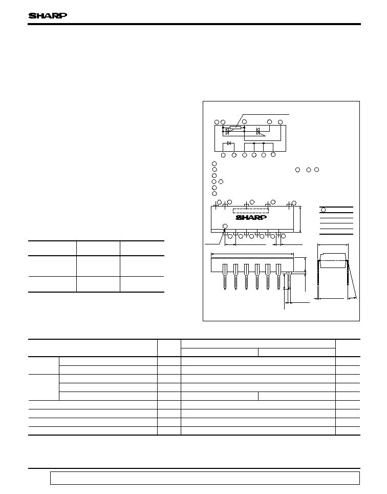
(Unit : mm )
16-Pin DIP Type SSR for Low
Power Control
2. RMS ON-state current I
T
: 1.2Arms
Parameter
Symbol
Unit
Input
Forward current
I
F
mA
Reverse voltage
V
R
V
Output
RMS ON-state current
I
T
*1
Peak one cycle surge current
I
surge
A
Repetitive peak OFF-state voltage
V
DRM
V
*2
Isolation voltage
V
iso
Operating temperature
T
opr
∞C
Storage temperature
T
stg
∞C
*3
Soldering temperature
T
sol
∞C
For 100V
lines
For 200V
lines
For phase control
No built-in zero-
cross circuit
S101D01
S201D01
Built-in zero-
cross circuit
S101D02
Internal connection diagram
2
3
4
5
6
7
9
2 Anode
3 Cathode
Gate
NC
A
Anode
mark
9
2
3
4
5
6
7
A (Model No.)
S101D01
S101D02
S201D01
S201D02
data books, etc. Contact SHARP in order to obtain the latest version of the device specification sheets before using any SHARP's device.
"
"
In the absence of confirmation by device specification sheets, SHARP takes no responsibility for any defects that occur in equipment using any of SHARP's devices, shown in catalogs,
S101D01/S101D02/S201D01/S201D02
(S101D02 , S201D02 )
S201D02
S201D01/S201D02
g
Zero-cross
circuit
s
Model Line-ups
Rating
S101D01/S101D02
S201D01/S201D02
50
6
1.2
12
400
600
- 25 to + 85
- 40 to + 125
260
A
rms
V
rms
*2 40 to 60% RH, AC 60Hz for 1 minute
4 000
4. Recognised by UL, file No. E94758
5. Approved by CSA, No. LR63705
g
Zero-cross circuit for
S101D02 /S201D02
T
1
T
2
:
0 to 13
∞
6.5
±
0.5
7.62
±
0.3
0.26
±
0.1
0.5
±
0.1
0.5
TYP.
3.5
±
0.5
1.2
±
0.2
2.54
±
0.25
19.82
±
0.5
3.4
±
0.5
16 15
16
15
13
13
11
11
16
15
13
11
9 ,
7
*To radiate the heat, solder
the lead pins
to
,
on
the pattern of the PWB
without using a socket such
that there is no open pin left.
4
9
s
Electrical Characteristics
(Ta = 25∞C )
S101D01/S101D02/S201D01/S201D02
Ambient temperature T
a
(∞C)
- 25
0
25
50
75
100
0
0.2
0.4
0.6
0.8
1.0
1.2
1.4
1.6
40
85
Ambient temperature T
a
(∞C)
Forward current I
F
(
mA
)
- 25
0
25
50
75
100
0
10
20
30
40
50
60
70
80
55
85
200
50
20
5
2
1
100
10
Forward voltage V
F
(V)
Forward current I
F
(
mA
)
0.5
0
1.0
1.5
2.0
2.5
3.0
-
25∞C
50∞C
25∞C
0∞C
Ambient temperature T
a
(∞C)
Minimum trigger current I
FT
(
mA
)
- 30
0
20
40
60
80
100
0
2
4
6
8
10
12
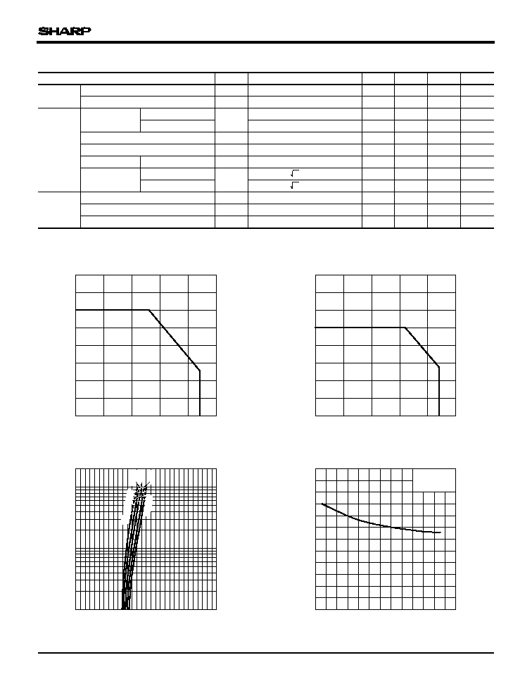
Fig. 1 RMS ON-state Current vs.
Ambient Temperature
Fig. 2 Forward Current vs.
Ambient Temperature
Fig. 3 Forward Current vs.
Forward Voltage
Fig. 4 Minimum Trigger Current vs.
Ambient Temperature
Parameter
Symbol
Conditions
MIN.
TYP.
MAX.
Unit
Input
Forward voltage
V
F
I
F
= 20mA
-
1.2
1.4
V
Reverse current
I
R
V
R
= 3V
-
-
10
- 5
A
Output
Repetitive
peak OFF-state
current
I
DRM
V
DRM
= 400V
-
-
10
- 4
A
V
DRM
= 600V
-
-
10
- 4
A
ON-state voltage
V
T
I
T
= 1.2A
-
-
1.7
V
Holding current
I
H
-
-
25
mA
Zero-cross voltage
V
OX
-
-
35
V
Critical rate of
rise of OFF-state
voltage
2
V
DRM
= 1/
∑ 400V
200
-
-
V/
µ
s
2
V
DRM
= 1/
∑ 600V
100
-
-
V/
µ
s
Transfer
charac-
teristics
Minimum trigger current
I
FT
V
D
= 6V, R
L
= 100
-
-
10
mA
Isolation resistance
R
ISO
5 x 10
10
10
11
-
Turn-on time
t
on
V
D
= 6V, R
L
= 100
, I
F
= 20mA
-
-
100
µ
s
( S101D01)
S101D01 / S101D02
S201D01 / S201D02
S101D02 / S201D02
S101D01 / S101D02
S201D01 / S201D02
RMS ON-state current I
T
(
Arms
)
V
D
= 6V
DC500V, 40 to 60% RH
V
D
= 6V
R
L
= 100
T
a
=
75∞C
dV/dt
Resistance load, I
F
= 15mA

Ambient temperature T
a
(∞C)
Minimum trigger current I
FT
(
mA
)
- 30
0
20
40
60
80
100
0
2
4
6
8
10
12
Ambient temperature T
a
(∞C)
Minimum trigger current I
FT
(
mA
)
- 30
0
20
40
60
80
100
0
2
4
6
8
10
12
Ambient temperature T
a
(∞C)
- 30
0
20
40
60
80
100
0.8
0.9
1.0
1.1
1.2
1.3
1.4
Ambient temperature T
a
(∞C)
- 30
0
20
40
60
80
100
T
(V)
0
0.5
1.0
1.5
0
0.2
0.4
0.6
0.8
1.0
1.2
Forward current I
F
( mA )
Turn-on time t
on
(
µ
s
)
10
10
20
30
40
50
100
20
30
40
50
100
60
70
80
90
S101D01/S101D02/S201D01/S201D02
Fig. 5 Minimum Trigger Current vs.
Ambient Temperature
Fig. 6 Minimum Trigger Current vs.
Ambient Temperature
Fig. 8 Relative Holding Current vs.
Ambient Temperature
(S101D02 , S201D02 )
(S201D01 )
Fig. 7 ON-state Voltage vs.
Ambient Temperature
Fig. 9 ON-state Current vs.
ON-state Voltage
(S101D01 )
Fig.10 Turn-on Time vs. Forward Current
ON-state voltage V
T
(V
)
Relative holding current I
H
(t∞C
)/I
H
(
25∞C
)
x
100(%
)
ON-state current I
T
(
A
)
ON-state voltage V
V
D
= 6V
R
L
= 100
V
D
= 6V
R
L
= 100
V
D
= 6V
10
3
10
2
10
1
I
T
= 1.2A
I
F
= 20mA
T
a
= 25∞C
V
D
= 6V
R
L
= 100
T
a
= 25∞C

S101D01/S101D02/S201D01/S201D02
Forward current I
F
( mA )
Turn-on time t
on
(
µ
s
)
20
20
10
30
40
50
100
10
30
40
50
100
Forward current I
F
( mA )
Turn-on time t
on
(
µ
s
)
20
30
100
10
30
40
50
100
20
40
50
200
Load
Z
S
SSR
2
D
1
R
1
+
V
CC
( 1) DC Drive
( 2) Pulse Drive
s
Basic Operation Circuit
Fig.11 Turn-on Time vs. Forward Current
Fig.12 Turn-on Time vs. Forward Current
Z
S
:
Surge absorption circuit
( 3) Phase Control
( Precautions for Use )
heat radiation from the mounted SSR.
pattern around increases the change of being affected by external noise.
1) All pins must be soldered since they are also used as heat sinks ( heat radiation fins ) . In designing, take into the
(S101D02 , S201D02 )
(S201D01)
AC 100V (S101D01 / S101D02 )
AC 200V (S201D01 / S201D02 )
Notes 1 ) If large amount of surge is loaded onto V
CC
or the driver circuit, add a diode D
1
2 ) Be sure to install a surge absorption circuit.
An appropriate circuit must be chosen according to the load ( for CR, choose its constant ) . This must be
carefully done especially for an inductive load.
3 ) For phase control, adjust such that the load current immediately after the input signal is applied will be
Tr1
V
AC supply voltage
Input signal
Load current
( for resistance load)
more than 60mA.
designing mounting pattern. The rounded part of Pin 15 ( gate ) must be as small as possible. Pulling the gate
2) For higher radiation efficiency that allows wider thermal margin, secure a wider round pattern for Pin 13 when
9
V
D
= 6V
R
L
= 100
T
a
= 25∞C
V
D
= 6V
R
L
= 100
T
a
= 25∞C
between terminals 2
and 3 to prevent reverse bias from being applied to the infrared LED.
3) As for other general cautions, refer to the chapter " Precautions for Use "
1
3
13
11

115
Application Circuits
NOTICE
qThe circuit application examples in this publication are provided to explain representative applications of
SHARP devices and are not intended to guarantee any circuit design or license any intellectual property
rights. SHARP takes no responsibility for any problems related to any intellectual property right of a
third party resulting from the use of SHARP's devices.
qContact SHARP in order to obtain the latest device specification sheets before using any SHARP device.
SHARP reserves the right to make changes in the specifications, characteristics, data, materials,
structure, and other contents described herein at any time without notice in order to improve design or
reliability. Manufacturing locations are also subject to change without notice.
qObserve the following points when using any devices in this publication. SHARP takes no responsibility
for damage caused by improper use of the devices which does not meet the conditions and absolute
maximum ratings to be used specified in the relevant specification sheet nor meet the following
conditions:
(i) The devices in this publication are designed for use in general electronic equipment designs such as:
--- Personal computers
--- Office automation equipment
--- Telecommunication equipment [terminal]
--- Test and measurement equipment
--- Industrial control
--- Audio visual equipment
--- Consumer electronics
(ii)Measures such as fail-safe function and redundant design should be taken to ensure reliability and
safety when SHARP devices are used for or in connection with equipment that requires higher
reliability such as:
--- Transportation control and safety equipment (i.e., aircraft, trains, automobiles, etc.)
--- Traffic signals
--- Gas leakage sensor breakers
--- Alarm equipment
--- Various safety devices, etc.
(iii)SHARP devices shall not be used for or in connection with equipment that requires an extremely
high level of reliability and safety such as:
--- Space applications
--- Telecommunication equipment [trunk lines]
--- Nuclear power control equipment
--- Medical and other life support equipment (e.g., scuba).
qContact a SHARP representative in advance when intending to use SHARP devices for any "specific"
applications other than those recommended by SHARP or when it is unclear which category mentioned
above controls the intended use.
qIf the SHARP devices listed in this publication fall within the scope of strategic products described in the
Foreign Exchange and Foreign Trade Control Law of Japan, it is necessary to obtain approval to export
such SHARP devices.
qThis publication is the proprietary product of SHARP and is copyrighted, with all rights reserved. Under
the copyright laws, no part of this publication may be reproduced or transmitted in any form or by any
means, electronic or mechanical, for any purpose, in whole or in part, without the express written
permission of SHARP. Express written permission is also required before any use of this publication
may be made by a third party.
qContact and consult with a SHARP representative if there are any questions about the contents of this
publication.