S102S03/S202S03
S102S03/S202S03
s
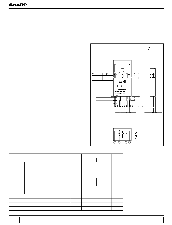
Outline Dimensions
( Unit : mm)
(Ta = 25 ∞C)
s
Features
s
Applications
s
Absolute Maximum Ratings
1. High radiation resin mold package
3. Isolation voltage between input and output
( V
iso
4. Low input driving current
1. Automatic vending machines
3. Amusement equipment
2. Programmable controllers
V
DSM
dI
T
/d
t
f
V
iso
T
opr
T
stg
T
sol
For 100V lines
For 200V lines
S102S03
S202S03
Operating frequency
*2
Isolation voltage
Operating temperature
Storage temperature
*3
Soldering temperature
Parameter
Symbol
Input
Forward current
I
F
Reverse voltage
V
R
Output
I
T
*1
Peak one cycle surge current
I
surge
V
DRM
( 36.0
)
(5.08) (7.62)
(2.54)
(1.4)
+
Internal connection diagram
( )
:
Typical dimensions
*
A
B
1
2
3
4
1
2
3 4
3 Input (
+
)
A (Model No.)
B
8A125VAC
8A250VAC
S102S03
S202S03
data books, etc. Contact SHARP in order to obtain the latest version of the device specification sheets before using any SHARP's device.
"
"
In the absence of confirmation by device specification sheets, SHARP takes no responsibility for any defects that occur in equipment using any of SHARP's devices, shown in catalogs,
RMS ON-state current
Repetitive peak OFF-state voltage
Non-repetitive peak OFF-state voltage
Critical rate of rise of ON-state current
1 Output (Triac T2 )
2 Output (Triac T1 )
2. RMS ON-state current I
T
: MAX. 8 Arms
at T
C
<= 80∞C ( With heat sink )
Rating
Unit
S102S03
S202S03
50
mA
6
V
*4
8
80
A
400
600
V
400
600
V
50
A/
µ
s
45 to 65
Hz
V
rms
- 25 to + 100
∞C
- 30 to + 125
∞C
260
∞C
( I
FT
: MAX. 5mA )
-
4 Input (
-
)
g
Do not allow external connection.
are common to terminal 1 .
* The metal parts marked *
5. Approved by CSA, No. LR63705
*1 50Hz sine wave,
(Note )
When the isolation voltage is
*3 For 10 seconds
SIP Type SSR with Mounting
Capability for External Heat
Sink
*4 T
C
<= 80∞C
A
rms
s
Model Line-ups
: 4 000V
rms
)
4 000
insulation sheet.
Tj = 25∞C start
*2 60Hz AC for 1 minute,
40 to 60% RH, Apply
voltages between input
and output by the
voltage tester with
zero-cross circuit.
( Input and output shall
be shorted respectively ) .
Recognized by UL, file No. E94758
dielectric withstand
necessary at using external
heat sink, please use the
18.5
±
0.2
16.4
±
0.3
3.2
±
0.2
3.2
±
0.2
5.5
±
0.2
5.0
±
0.3
19.6
±
0.2
11.2
MIN.
4.2
MAX.
g
0.2
MAX.
4
-
1.1
±
0.2
4
-
0.8
±
0.2
4
-
1.25
±
0.3
0.6
±
0.1
( Ta = 25∞C)
Parameter
Symbol
Input
Forward voltage
V
F
Reverse current
I
R
Output
I
DRM
On-state voltage
V
T
Holding current
I
H
Critical rate of rise of com-
Transfer
charac-
teristics
Minimum trigger current
I
FT
Isolation resistance
R
ISO
Turn-on time
Turn-off time
Thermal resistance ( Between junction and case )
Thermal resistance ( Between junction and ambience)
Conditions
I
F
= 20mA
V
R
= 3V
V
D
= V
DRM
I
T
= 2A
rms
V
D
= 2/3V
DRM
V
D
= 12V, R
L
= 30
AC = 50Hz
R
th(j - c)
R
th(j - a)
MIN.
TYP.
MAX.
Unit
-
1.2
1.4
V
-
-
10
-
4
A
-
-
10
-
4
A
-
-
1.5
V
rms
-
-
-
35
mA
30
-
-
V/
µ
s
5
-
-
V/
µ
s
-
-
5
mA
10
10
-
-
1
ms
-
-
-
-
10
ms
-
4.5
-
∞C/W
-
-
-
40
-
∞C/W
t
on
t
off
Repetitive peak OFF-state current
Critical rate of rise of OFF-state voltage
mutating OFF-state voltage
2
- 25
0
1
75
25
0
50
125
100
9
3
4
5
6
7
8
10
(2)
(4)
(6)
(5)
(3)
(1)
carried out.
conductive silicone grease on the heat sink
the device at the center of the Al heat sink
( 5) With heat sink ( 50 x 50 x 2 mm Al plate )
( 4) With heat sink ( 75 x 75 x 2 mm Al plate )
( 3) With heat sink ( 100 x 100 x 2 mm Al plate )
( 2) With heat sink ( 200 x 200 x 2 mm Al plate )
( 6) Without heat sink
( 1) With infinite heat sink
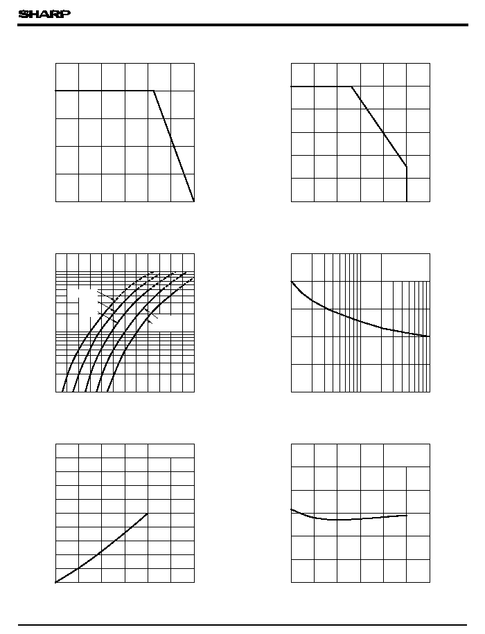
Fig. 1 RMS ON-state Current vs.
Ambient Temperature
S102S03/S202S03
s
Electro-optical Characteristics
RMS ON-state current I
T
(
A
rms
)
Ambient temperature T
a
(∞C)
V
D
= 400V
Tj = 125∞C, dIt/d
t
= - 4.0A/ms,
mounting plate. Forcible cooling shall not be
with a torque of 0.4N ∑ m and apply thermal
dV/dt
( dV/dt )
C
DC = 500V, 40 to 60 % RH
( Note) With the Al heat sink set up vertically, tighten
Resistance load, I
F
= 20mA
S102S03/S202S03
RMS ON-state current I
T
( A
rms
)
4
Maximum ON-state power dissipation
(W
)
6
2
0
0
4
2
10
8
12
18
10
8
6
16
14
12
20
50
Surge current I
surge
(
A
)
1
0
20
2
10
5
20
100
40
60
80
100
Ambient temperature T
a
(∞C)
Forward current I
F
(
mA
)
- 25
0
25
50
75
100
125
0
10
20
30
40
50
60
Ambient temperature T
a
(∞C)
Minimum trigger current I
FT
(
mA
)
- 25
0
25
50
75
100
125
0
1
2
3
4
5
6
Forward voltage V
F
(V)
Forward current I
F
(
mA
)
0.9
1
1.1
1.0
1.2
10
2
5
20
50
100
25∞C
50∞C
1.3
1.4
1.5
- 25∞C
0∞C
Fig. 3 Forward Current vs.
Ambient Temperature
Fig. 4 Forward Current vs.
Forward Voltage
Fig. 5 Surge Current vs.
Fig. 7 Minimum Trigger Current vs. Ambient
Temperature (Typical Value)
Case temperature T (∞C)
- 25
0
25
50
75
100
125
0
2
4
6
8
10
Fig. 2 RMS ON-state Current vs.
Case Temperature
Power-on Cycle
Power-on cycle ( Times )
c
RMS ON-state current I
T
(
Arms
)
vs. RMS ON-state Current
Fig. 6 Maximum ON-state Power Dissipation
f = 50Hz
T
j
= 25∞C Start
T
a
= 75∞C
T
a
= 25∞C
V
D
= 12V
R
L
= 30
(Typical Value)
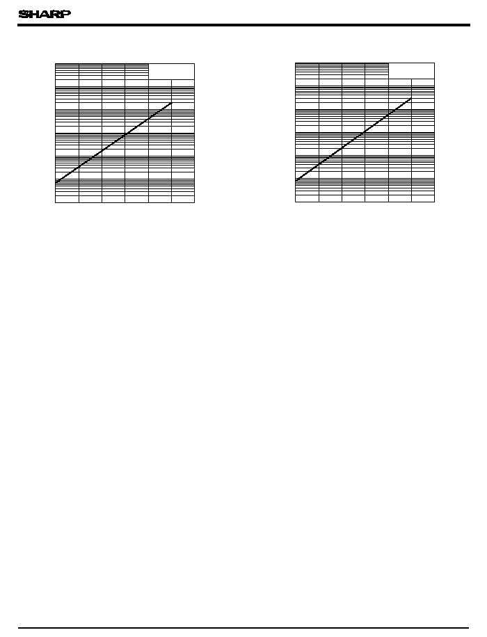
S102S03/S202S03
Ambient temperature T
a
(∞C)
- 25
0
25
50
75
100
125
10
- 9
10
- 8
10
- 7
10
- 6
10
- 5
10
- 4
10
- 3
Ambient temperature T
a
(∞C)
10
- 5
10
- 6
10
- 7
10
- 8
10
- 9
- 25
0
25
10
- 3
10
- 4
100
75
50
125
Ambient Temperature (Typical Value )
Fig.8-a Repetitive Peak OFF-state Current vs.
Ambient Temperature (Typical Value)
Fig.8-b Repetitive Peak OFF-state Current vs.
(S102S03 )
(S202S03 )
V
D
= 400V
Repetitive peak OFF-state current I
DRM
(
A
)
V
D
= 600V
Repetitive peak OFF-state current I
DRM
(
A
)
q Please refer to the chapter " Precautions for Use "