 | –≠–ª–µ–∫—Ç—Ä–æ–Ω–Ω—ã–π –∫–æ–º–ø–æ–Ω–µ–Ω—Ç: S21MD10V | –°–∫–∞—á–∞—Ç—å:  PDF PDF  ZIP ZIP |
S21MD10V
S21MD10V
s
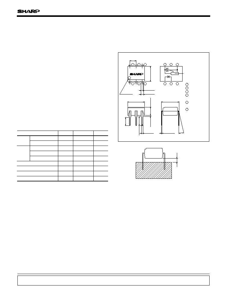
Outline Dimensions
(Unit : mm)
Built-in Zero-cross Circuit, High
Noise Resistance Type
Phototriac Coupler
Anode
mark
Internal connection
diagram
Zero-cross
circuit
6.5
±
0.5
2.54
±
0.25
0.9
±
0.2
1.2
±
0.3
7.62
±
0.3
0.26
±
0.1
0.5
±
0.1
0.5
TYP.
3.5
±
0.5
7.12
±
0.5
3.7
±
0.5
3.35
±
0.5
: 0 to 13∞
1
2
3
4
5
6
Anode
Cathode
NC
Anode/
Cathode
No external
connection
Anode/
Cathode
1
2
3
6
5
4
1
2
3
6
5
4
S21MD10V
Notice
In the absence of confirmation by device specification sheets, SHARP takes no responsibility for any defects that may occur in equipment using any SHARP
devices shown in catalogs, data books, etc. Contact SHARP in order to obtain the latest device specification sheets before using any SHARP device.
Internet
Internet address for Electronic Components Group http://www.sharp.co.jp/ecg/
1mm
Soldering area
s
Absolute Maximum Ratings
1. For triggering medium/high power triac
s
Features
s
Applications
1. Built-in zero-cross circuit
2. High critical rate of rise of OFF-state voltage
(dV/dt:MIN. 1 000V/
µ
s)
3. High repetitive peak OFF-state voltage (V
DRM
:MIN. 600V)
4. Isolation voltage between input and output
(V
iso (rms)
:5kV)
5. Recognized by UL, file No.E64380
DIN-VDE 0884 approved type is also available as an option
Approved by VDE, No.104842
S21MD10V
is for 200V line
*1 50Hz Sine wave
*2 40 to 60% RH, AC for 1 min, f
=
60HZ
*3 For 10s
Parameter
Symbol
Rating
Unit
Input
Output
(Ta
=
25∞C)
Forward current
50
Reverse voltage
6
RMS ON-state current
0.1
1.2
Repetitive peak OFF-state voltage
600
Operating temperature
-
30 to
+
100
Storage temperature
-
55 to
+
125
260
*3
Soldering temperature
*2
Isolation voltage
*1
Peak one cycle surge current
5
I
F
V
R
I
T (rms)
I
surge
V
DRM
V
iso (rms)
T
opr
T
stg
T
sol
mA
V
A
V
∞C
∞C
∞C
A
kV
Parameter
Symbol
Unit
Input
Forward voltage
V
F
V
I
R
V
R
=
3V
A
Reverse current
I
DRM
A
Repetitive peak OFF-state current
V
T
I
T
=
100mA
V
D
=
6V
Resistance load, I
F
=
10mA
V
V
Output
On-state voltage
I
H
mA
dV/dt
I
FT
V
OX
mA
R
ISO
t
on
µ
s
Transfer
charac-
ter istics
I
F
=
20mA
V
DRM
=
Rated
MIN.
-
-
-
0.1
-
-
-
5
◊
10
10
10
-
5
10
-
6
-
-
-
MAX.
3.0
3.5
5
20
-
35
1.4
Conditions
V
D
=
6V, R
L
=
100
DC500V, 40 to 60%RH
V
D
=
6V, R
L
=
100
, I
F
=
20
m
A
TYP.
-
V/
µ
s
1 000
2 000
-
-
1
◊
10
11
1.2
-
-
-
Holding current
Critical rate of rise of OFF-state voltage
Minimum trigger current
Zero-cross voltage
Isolation resistance
Turn-on time
(Ta
=
25∞C)
V
DRM
=
1/ 2 Rated
S21MD10V
s
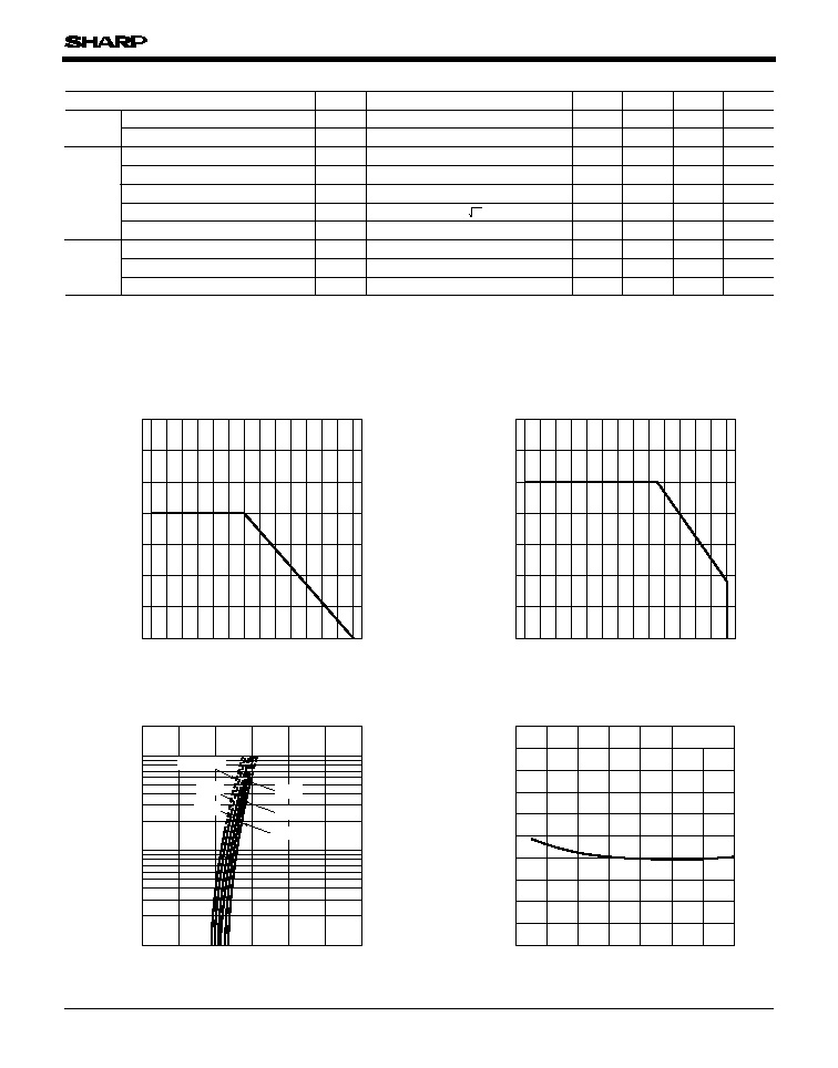
Electro-optical Characteristics
0
25
50
75
100
125
150
175
-
30
-
20
-
10 0 10 20 30 40 50 60 70 80 90 100
RMS ON-state current I
r (rms)
(mA)
Ambient temperature T
a
(∞C)
0
10
20
30
40
50
60
70
-
30
-
20
-
10 0 10 20 30 40 50 60 70 80 90 100
Forward current I
F
(mA)
Ambient temperature T
a
(∞C)
Fig.1
RMS ON-state Current vs. Ambient
Temperature
Fig.2
Forward Current vs. Ambient
Temperature
1
2
5
10
200
0
1
0.5
1.5
2
2.5
3
20
50
100
Forward current I
F
(mA)
Forward voltage V
F
(V)
T
a
=100∞C
25∞C
75∞C
50∞C
0∞C
-
30∞C
Fig.3
Forward Current vs. Forward Voltage
0
1
2
3
4
5
6
7
8
9
10
-
40
0
-
20
20
40
60
80
100
Minimum trigger current I
FT
(mA)
Ambient temperature T
a
(∞C)
V
D
=
4V
Fig.4
Minimum Trigger Current vs. Ambient
Temperature

S21MD10V
1
1.1
1.2
1.3
1.4
1.5
1.6
1.7
1.8
1.9
2
2.1
2.2
2.3
2.4
2.5
-
40
0
-
20
20
40
60
80
100
ON-state voltage V
T
(V)
Ambient temperature T
a
(∞C)
I
T
=
100mA
0.01
0.1
1
-
40
0
-
20
20
40
60
80
100
Holding current I
H
(mA)
Ambient temperature T
a
(∞C)
V
D
=
4V
Fig.5
ON-state Voltage vs. Ambient
Temperature
Fig.7
Repetitive Peak OFF-state Current vs.
Ambient Temperature
Fig.6
Holding Current vs. Ambient
Temperature
0.001
0.1
10
-
40
0
-
20
20
40
60
80
100
Repetitive peak OFF-state current I
DRM
(
µ
A)
Ambient temperature T
a
(∞C)
1
0.01
V
D
=
600V
Fig.8 Relative Repetitive Peak OFF-state
Voltage vs. Ambient Temperature
0.7
0.8
0.9
1
1.1
1.2
1.3
-
40
0
-
20
20
40
60
80
100
Relative repetitive peak OFF-state voltage
V
DRM
(T
j
=
T
a
) / V
DRM
(T
j
=
25
∞
C)
Ambient temperature T
a
(∞C)
10
100
1 000
1
10
100
Turn-on time t
ON
(
µ
s)
Forward current I
F
(mA)
V
D
=
6V
R
L
=
100
T
a
=
25∞C
Fig.9
Turn-on Time vs. Forward Current
0
2
4
6
8
10
12
14
16
18
20
-
40
0
-
20
20
40
60
80
100
Zero-cross voltage V
OX
(V)
Ambient temperature T
a
(∞C)
R load, I
F
=
15mA
Fig.10
Zero-cross Voltage vs. Ambient
Temperature

S21MD10V
Fig.11 Basic Operation Circuit
Load
Note) Please use on condition of the triac for power triggers.
Zero-
cross
circuit
+
V
CC
V
IN
AC200V
6
5
4
1
2
3
Medium/High Power Triac Drive Circuit

115
Application Circuits
NOTICE
qThe circuit application examples in this publication are provided to explain representative applications of
SHARP devices and are not intended to guarantee any circuit design or license any intellectual property
rights. SHARP takes no responsibility for any problems related to any intellectual property right of a
third party resulting from the use of SHARP's devices.
qContact SHARP in order to obtain the latest device specification sheets before using any SHARP device.
SHARP reserves the right to make changes in the specifications, characteristics, data, materials,
structure, and other contents described herein at any time without notice in order to improve design or
reliability. Manufacturing locations are also subject to change without notice.
qObserve the following points when using any devices in this publication. SHARP takes no responsibility
for damage caused by improper use of the devices which does not meet the conditions and absolute
maximum ratings to be used specified in the relevant specification sheet nor meet the following
conditions:
(i) The devices in this publication are designed for use in general electronic equipment designs such as:
--- Personal computers
--- Office automation equipment
--- Telecommunication equipment [terminal]
--- Test and measurement equipment
--- Industrial control
--- Audio visual equipment
--- Consumer electronics
(ii)Measures such as fail-safe function and redundant design should be taken to ensure reliability and
safety when SHARP devices are used for or in connection with equipment that requires higher
reliability such as:
--- Transportation control and safety equipment (i.e., aircraft, trains, automobiles, etc.)
--- Traffic signals
--- Gas leakage sensor breakers
--- Alarm equipment
--- Various safety devices, etc.
(iii)SHARP devices shall not be used for or in connection with equipment that requires an extremely
high level of reliability and safety such as:
--- Space applications
--- Telecommunication equipment [trunk lines]
--- Nuclear power control equipment
--- Medical and other life support equipment (e.g., scuba).
qContact a SHARP representative in advance when intending to use SHARP devices for any "specific"
applications other than those recommended by SHARP or when it is unclear which category mentioned
above controls the intended use.
qIf the SHARP devices listed in this publication fall within the scope of strategic products described in the
Foreign Exchange and Foreign Trade Control Law of Japan, it is necessary to obtain approval to export
such SHARP devices.
qThis publication is the proprietary product of SHARP and is copyrighted, with all rights reserved. Under
the copyright laws, no part of this publication may be reproduced or transmitted in any form or by any
means, electronic or mechanical, for any purpose, in whole or in part, without the express written
permission of SHARP. Express written permission is also required before any use of this publication
may be made by a third party.
qContact and consult with a SHARP representative if there are any questions about the contents of this
publication.