 | –≠–ª–µ–∫—Ç—Ä–æ–Ω–Ω—ã–π –∫–æ–º–ø–æ–Ω–µ–Ω—Ç: S21MD3TV | –°–∫–∞—á–∞—Ç—å:  PDF PDF  ZIP ZIP |
S21MD4TV
S11MD5T/S21MD3TV/
Phototriac Coupler
s
Applications
s
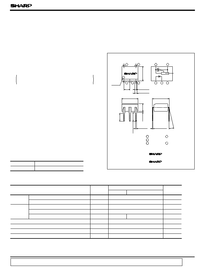
Outline Dimensions
s
Features
1. NO.5 pin completely sealed in the mold for
external noise resistance
1 Sine wave
3 For 10 seconds
s
Absolute Maximum Ratings
(Ta = 25∞C)
100V
S11MD5T
200V
Parameter
Symbol
Rating
Unit
S11MD5T
Input
I
F
50
mA
Reverse voltage
V
R
6
V
Output
I
T
0.1
1
Peak one cycle surge current
I
surge
1.2
A
V
DRM
400
600
V
2
Isolation voltage
V
iso
Operating temperature
T
opr
- 30 to + 100
∞C
Storage temperature
T
stg
- 55 to + 125
∞C
3
Soldering temperature
T
sol
260
∞C
S11MD5T
V
DRM
: MIN. 400V
RMS ON-state current
Repetitive peak OFF-state voltage
S11MD5T
diagram
Internal connection
S21MD4TV
1
2
3
4
6
1
2
3
6
4
g
Zero-cross
circuit
Anode
mark
S21MD3T
S21MD4T
1 Anode
2 Cathode
3 NC
4 Anode/
Cathode
6 Anode/
Cathode
data books, etc. Contact SHARP in order to obtain the latest version of the device specification sheets before using any SHARP's device.
"
"
In the absence of confirmation by device specification sheets, SHARP takes no responsibility for any defects that occur in equipment using any of SHARP's devices, shown in catalogs,
5. Recognized by UL : recognized, file No. E64380
S11MD5T/S21MD3TV/S21MD4TV
2. Built-in zero-cross circuit
(S21MD4TV)
S21MD3TV/S21MD4TV
V
DRM
: MIN. 600V
S11MD5T/S21MD3TV
( Unit : mm)
S21MD3TV/S21MD4TV
S21MD3TV/S21MD4TV
High Noise-resistance Type
4. Isolation voltage between input and output
1. For triggering of power triac
Forward current
( Viso : 5 000 Vrms )
s
Model Line-ups
5 000
2 40 to 60% RH, AC for 1 minute, f = 60Hz
A
rms
V
rms
Marking of S21MD3TV
:
Marking of S21MD4TV
:
g
Zero-cross circuit (S21MD4TV )
:
0 to 13
∞
6.5
±
0.5
0.9
±
0.2
1.2
±
0.3
2.54
±
0.25
7.12
±
0.5
7.62
±
0.3
3.5
±
0.5
0.5
TYP.
0.5
±
0.1
0.26
±
0.1
3.7
±
0.5
3.35
±
0.5
3. High repetitive peak OFF-state voltage.
S11MD5T/S21MD3TV/S21MD4TV
s
Electro-optical Characteristics
( Ta= 25∞C)
- 30
0
20
40
60
80
100
0
0.05
0.10
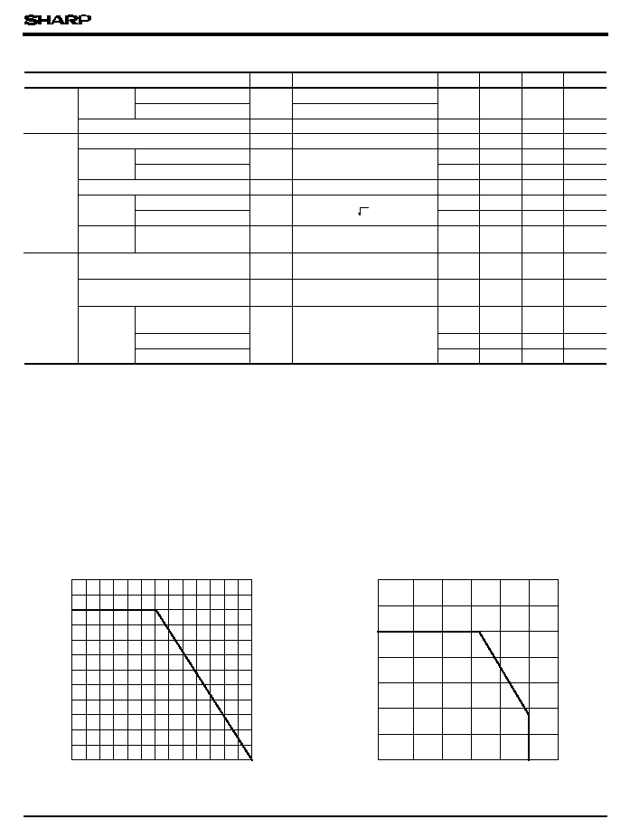
Fig. 1 RMS ON-state Current vs.
Ambient Temperature
Ambient temperature T
a
(∞C )
- 30
0
25
50
75
100
125
0
10
20
30
40
50
60
70
Fig. 2 Forward Current vs.
Ambient Temperature
Forward current I
F
(
mA
)
Ambient temperature T
a
(∞C)
T
Symbol
Conditions
MIN.
TYP.
MAX.
Forward
voltage
S11MD5T/S21MD4TV
V
F
I
F
= 20mA
-
1.2
1.4
I
F
= 30mA
S21MD3TV
Reverse current
I
R
V
R
= 3V
-
-
10
-5
Repetitive peak OFF-state current
I
DRM
V
DRM
= R
ated
-
-
10
-6
ON-state
voltage
S11MD5T
V
T
I
T
= 0.1A
-
1.3
2.0
-
1.7
2.5
S21MD3TV/S21MD4TV
Holding current
I
H
V
D
= 6V
0.1
1
3.5
Critical rate
of rise of OFF-
state voltage
S11MD5T/S21MD4TV
V
DRM
= 1/ 2 Rated
100
-
-
500
-
-
S21MD3TV
Zero-cross
voltage
S21MD4TV
V
OX
I
F
= 15mA
-
-
35
Minimun trigger current
I
FT
V
D
= 6V
R
L
= 100
-
-
10
Isolation resistance
R
ISO
DC500V
5 x 10
10
10
11
-
Turn-on
time
S11MD5T
t
on
-
80
200
S21MD3TV
-
100
-
50
Unit
V
A
A
V
V
mA
V/
µ
s
V/
µ
s
V
mA
µ
s
µ
s
µ
s
Parameter
Input
Output
Transfer
charac-
teristics
R
L
= 100
-
20
S21MD4TV
V
D
= 6V, I
F
= 20mA
RMS ON-state current I
40 to 60% RH
dV/dt
Resistance load
4
S21MD3TV
: I
F
=30mA
4

S11MD5T/S21MD3TV/S21MD4TV
Forward current I
F
(
mA
)
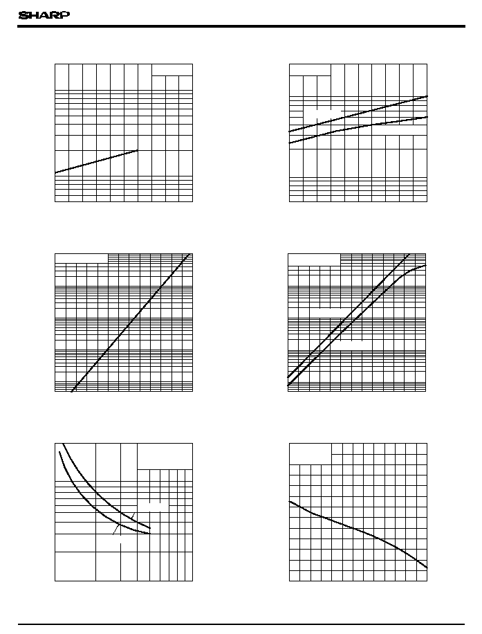
Fig. 3 Forward Current vs. Forward Voltage
S21MD4TV
S21MD3TV
S11MD5T
8
6
4
2
100
80
60
40
20
0
0
-30
Fig. 4 Minimum Trigger Current vs.
Ambient Temperature
a
(∞C)
- 30
0.7
0
20
40
60
80
100
0.8
0.9
1.0
1.1
1.2
1.3
S21MD3TV
S11MD5T
S21MD4TV
- 30
0
20
40
60
80
100
1.0
1.1
1.2
1.3
1.4
1.5
1.6
T
(
V
)
Ambient temperature T
a
(∞C)
1.4
1.5
- 30
0
20
100
1.6
1.7
1.8
1.9
2.0
40
60
80
S21MD3TV
S21MD4TV
T
(
V
)
Ambient temperature T
a
(∞C)
-30
100
0.1
0.2
0.5
1
2
5
10
80
60
40
20
0
S11MD5T
S21MD3TV
S21MD4TV
Ambient temperature T
a
(∞C)
Fig. 7 Holding Current vs.
Ambient Temperature
Holding current I
H
(
mA
)
Fig. 5 Relative Repetitive Peak OFF-state
Voltage vs. Ambient Temperature
V
DRM
(
T=
T
a
)
/V
DRM
(
T
=
25∞C
)
Ambient temperature T
a
(∞C)
Ambient Temperature
(S21MD3TV/S21MD4TV)
Ambient temperature T
Minimum trigger current I
FT
(
mA
)
V
D
= 6V
R
L
= 100
Forward voltage V
F
(V)
14
10
12
Fig. 6-a ON-state Voltage vs.
Ambient Temperature
(S11MD5T)
Relative repetitive peak OFF-state voltage
j
ON-state voltage V
Fig. 6-b ON-state Voltage vs.
ON-state voltage V
j
I
T
= 100mA
I
T
= 100mA
V
D
= 6V
200
10
5
2
1
0
0.5
1.0
1.5
2.5
3.0
2.0
100
20
50
75∞C
50∞C
25∞C
0∞C
- 30∞C
T
a
= 100∞C
S11MD5T/S21MD3TV/S21MD4TV
100
200
300
400
500
600
5
10
- 10
2
5
10
- 9
2
5
100
200
300
400
500
600
10
- 8
2
5
2
10
- 7
S21MD4TV
S21MD3TV
vs. OFF-state Voltate
- 30
0
20
40
60
80
100
5
10
- 11
2
5
2
5
2
5
2
5
10
- 10
10
- 9
10
- 8
10
- 7
Ambient temperature T
a
(∞C)
- 30
0
100
10
- 5
10
- 6
10
- 7
10
- 8
10
- 9
5
2
5
2
5
2
5
20
40
60
80
S21MD3TV
S21MD4TV
vs. Ambient Temperature
Ambient temperature T
a
(∞C)
2
5
100
80
60
40
20
0
15
-30
20
25
R load
Zero-cross voltage V
OX
(
V
)
100
10
200
50
100
20
20
50
S11MD5T
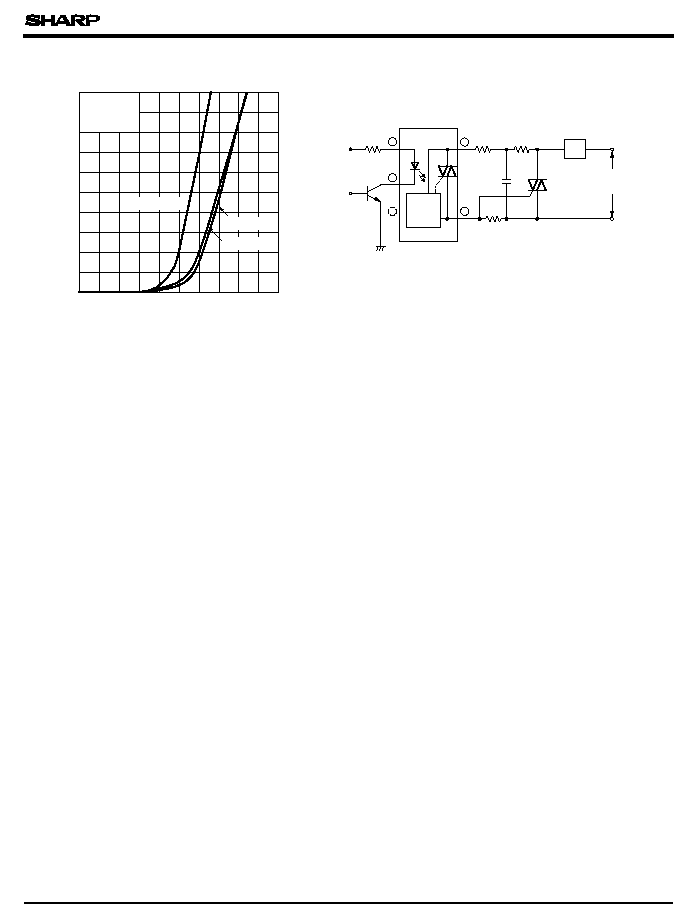
Fig.10 Turn-on Time vs. Forward Current
Turn-on time t
on
(
µ
s
)
D
(V)
DRM
(
A
)
DRM
(
A
)
DRM
(
A
)
vs. OFF-state Voltage
(S11MD5T)
D
(V)
(S21MD3TV/S21MD4TV)
(S11MD5T)
(S21MD3TV/S21MD4TV)
Forward current I
F
( mA )
(S11MD5T/S21MD3TV )
Ambient temperature T
a
(∞C)
Fig.11 Zero-cross Voltage vs.
Ambient Temperature
(S21MD4TV)
Repetitive peak OFF-state current I
Fig. 8-a Repetitive Peak OFF-state Current
Fig. 8-b Repetitive Peak OFF-state Current
Repetitive peak OFF-state current I
Fig. 9-a Repetitive Peak OFF-state Current
Fig. 9-b Repetitive Peak OFF-state Current
Repetitive peak OFF-state current I
Repetitive peak OFF-state current I
DRM
(A
)
S21MD3TV
T
a
= 25∞C
T
a
= 25∞C
V
DRM
= Rated
V
DRM
= Rated
T
a
= 25∞C
R
L
= 100
V
D
= 6V
I
F
= 15mA
OFF-state voltage V
vs. Ambient Temperature
OFF-state voltage V
S11MD5T/S21MD3TV/S21MD4TV
0
10
0
S21MD3TV
0.2 0.4 0.6 0.8 1.0 1.2 1.4 1.6 1.8 2.0
20
30
40
50
60
70
80
90
100
S21MD4TV
S11MD5T
Fig.12 ON-state Current vs.
T
(
mA
)
V
T
(V)
Zero-
cross
Circuit
+
V
CC
V
IN
Load
1
2
3
6
4
s
Basic Operation Circuit
AC100V
:
S11MD5T
AC200V
:
S21MD3TV
S21MD4TV
S21MD4TV
.
ON-state Voltage
ON-state voltage
Zero-cross circuit is applied to
Medium/High Power Triac Drive Circuit
ON-state current I
Note ) Please use on condition of the triac for power triggers.
I
F
= 20mA
T
a
= 25∞C
q
Please refer to the chapter "Precautions for Use."