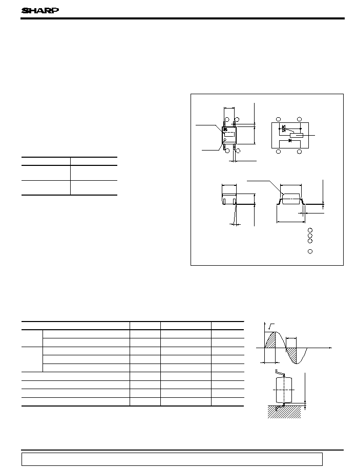
Outline Dimensions
(Unit : mm)
Features
Application
Model Line-ups
C0.4
1
*
6
∞
4.4
±
0.2
0.4
±
0.1
3.6
±
0.3
2.6
±
0.2
0.1
±
0.1
5.3
±
0.3
0.2
±
0.05
7.0
+
0.2
-
0.7
0.5
+
0.4
-
0.2
0.6
MAX.
Zero-cross
circuit
Model No.
Anode
mark
(Input side)
(Ta=25∞C)
(A)
0
2
∑
I
T
2
I
T
1
360
∞
90
∞
180
∞
1
,
2
<=
90
∞
Absolute Maximum Ratings
3
4
4
3
2
2
Internal connection diagram
S2S3/S2S4
S2S3/S2S4
Mini-Flat Type
Phototriac Coupler
1 Anode
4 Anode/
Cathode
Zero-cross circuit
not built in
S2S3
Zero-cross circuit
built in
S2S4
1. For SSR
*
The zero-cross circuit for S2S4
For 100/200V line
3 Anode/
Cathode
2 Cathode
Soldering area
0.2 mm or more
Rating
Forward current
I
F
50
mA
Reverse voltage
V
R
6
V
RMS ON-state current
*1
I
T
0.05
A
rms
*2
Peak one cycle surge current
I
surge
0.6 (50Hz sine wave)
A
Repetitive peak OFF-state voltage
V
DRM
600
V
Isolation voltage
*3
V
iso
3 750
V
rms
Operating temperature
T
opr
- 30 to+100
∞C
Storage temperature
T
stg
- 40 to+125
∞C
*4
T
sol
260
∞C
Input
Output
Symbol
Unit
Parameter
2.54
±
0.25
1. Popular type
2. Small package type
3. Conforming to UL double protective insulation (V
iso
: 3 750V
rms
)
4. Infrared reflow soldering type (230∞C, within 30 seconds)
Soldering temperature
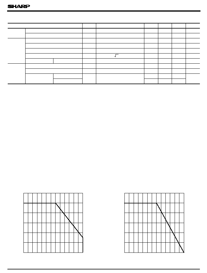
*1 The definition of conduction angle
of RMS ON-state current I
T
should be as shown in the right drawing. For decrease curve, refer to Fig. 2.
*2 50Hz sine curve
*3 40 to 60% RH, AC for 1 minute
*4 For 10 seconds
5. Recognized by UL (No
.
64380)
1
s
s
s
s
s
data books, etc. Contact SHARP in order to obtain the latest version of the device specification sheets before using any SHARP's device.
"
"
In the absence of confirmation by device specification sheets, SHARP takes no responsibility for any defects that occur in equipment using any of SHARP's devices, shown in catalogs,
(Ta=25∞C)
Electro-optical Characteristics
0
10
- 30
0
50
100
20
30
40
50
60
- 30
0
0
50
100
10
20
30
40
50
60
MIN.
TYP.
MAX.
Input
Forward voltage
V
F
I
F
= 20mA
-
1.2
1.4
V
Reverse current
I
R
V
R
= 3V
-
-
10
µ
A
Output
Repetitive peak OFF-state current
I
DRM
-
-
1
µ
A
ON-state voltage
V
T
I
T
= 0.05A
-
-
2.5
V
Holding current
I
H
V
D
= 6V
0.1
-
3.5
mA
Critical rate of rise of OFF-state voltage
2
V
DRM
= 1/
∑ Rated
100
-
V/
µ
s
Zero-cross voltage
S2S4
V
OX
I
F
= 15mA, Resistance load
-
-
35
V
Transfer
characteristics
I
FT
V
D
= 6V, R
L
= 100
-
-
10
mA
Insulation resistance
R
ISO
DC500V, 40 to 60% RH
5 x 10
10
11
1 x 10
-
Turn-on time
S2S3
t
on
V
D
= 6V, R
L
= 100
,
I
F
= 20mA
-
-
100
µ
s
S2S4
-
-
50
S2S3/S2S4
Minimum trigger current
V
DRM
= Rated
Fig. 1 Forward Current vs. Ambient
Temperature
Fig. 2 RMS ON-state Current vs. Ambient
Temperature
Forward current I
F
(mA)
Ambient temperature Ta (∞C)
Ambient temperature Ta (∞C)
1 000
Symbol
Unit
Parameter
Conditions
dv/dt
RMS ON-state current I
T
(mArms)
s