- 1 -
SM8521 CONTENTS
DESCRIPTION .............................................................. 2
FEATURES .................................................................... 2
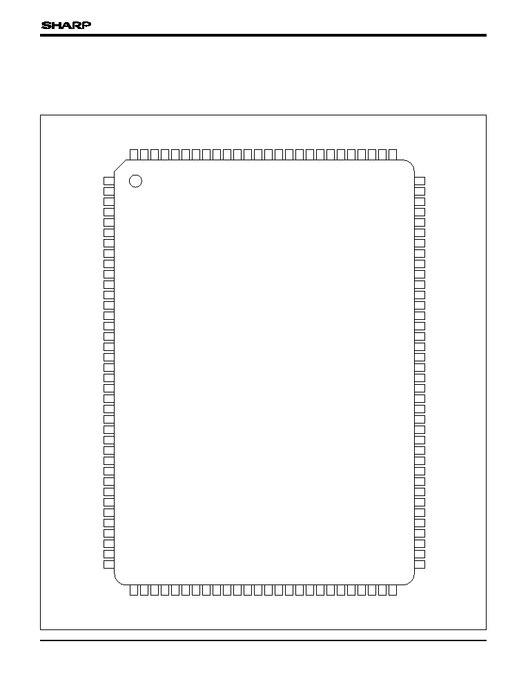
PIN CONNECTIONS ..................................................... 3
BLOCK DIAGRAM ....................................................... 4
PIN DESCRIPTION ....................................................... 5
ABSOLUTE MAXIMUM RATINGS ............................. 6
RECOMMENDED OPERATING CONDITIONS ............. 6
DC CHARACTERISTICS ............................................. 7
SM85CPU ...................................................................... 8
Register Lineup
Address Space
ROM Area
Register File Area
RAM Area
Data Format
Bus Timing
SYSTEM CONTROL .................................................. 18
Oscillator Circuit
Clock System
Memory Map
Hardware Reset
Interrupt Function
Standby Function
I/O PORTS ................................................................... 29
TIMER/COUNTERS .................................................... 30
Clock Timer
Watchdog Timer Register (WDT)
LCDC/DMA .................................................................. 33
VRAM Configuration
DMA Transfer
Compound and Overwrite Mode
Registers
SOUND GENERATOR ............................................... 41
Sound Waveform Register
Registers
MMU ............................................................................. 45
UNIVERSAL ASYNCHRONOUS RECEIVER AND
TRANSMITTER (UART) INTERFACE ......................... 47
UART Transmit Data Register (URTT)
UART Receive Data Register (URTR)
UART Status Register (URTS)
UART Control Register (URTC)
Transfer Format
INSTRUCTION SET .................................................... 51
Definition of Symbols
Instruction Summary
Addressing Mode
SYSTEM CONFIGURATION EXAMPLE .................. 55
SM8521
DESCRIPTION
The SM8521 is a CMOS 8-bit single-chip micro-
computer containing SM85CPU core and the required
peripheral functions for dot matrix LCD display
system. SM85CPU is an 8-bit High performance CPU
with various addressing modes and High-efficiency
instruction sets. SM85CPU is featured by allocating
general registers on RAM to reduce overhead when
calling subroutines.
The peripheral functions and memory of SM8521
contain ROM, RAM, MMU, LCD controller, DMA,
sound generator, timer, serial interface (UART) and
PIO.
FEATURES
� ROM capacity : 4 096 x 8 bits
� RAM capacity : 1 024 x 8 bits
� External memory expansion
� A RAM area is used as subroutine stack
� CPU core :
� 8 bits x 8 ports (or 16 bits x 4 ports) and 16
bits x 4 ports general purpose register are
used as accumulator, register pointer, and
register index.
� Instruction sets
67
(multiplication/division/bit manipulation instruc-
tion)
� Addressing mode
23 types
� System clock cycle 0.2 �s (MIN.) at 10 MHz
main clock cycle
� System clock is variable by software (system
clock can be optioned to 1/2, 1/4, 1/8, 1/16,
1/32 of main-clock and 1/2 of sub-clock.)
� Built-in main clock oscillator for system clock
� Built-in sub clock oscillator for real time clock
� Interrupts :
Non-maskable interrupts
x 2
Maskable interrupts
x 8
� Standby modes : Halt mode/Stop mode
� I/O ports : Input/output 32
� Timer :
8 bits x 2 (with 8 bits prescaller)
Clock timer x 1 (1 s or 1 min)
Watchdog timer
� MMU :
In each 8 k-byte unit, external memory can be
expanded up to MAX. 2 M bytes.
� LCD controller :
Display size 160 x 100 dots
160 x 160 dots
160 x 200 dots
200 x 100 dots
200 x 160 dots
black & white 4 gradations
(interframe elimination)
VRAM
160 x 200 dot x 2 phases or
200 x 160 dot x 2 phases
(required externally)
� DMA :
Transmission mode : ROM to VRAM,
VRAM to VRAM,
Extend RAM to VRAM,
VRAM to Extend RAM
Transmission data : Rectangle (Arbitrary size)
� Sound generator :
Arbitrary waveform x 2 (16-level tone, 32-
step/1-period waveform output)
Noise x 1 channel
� PIO :
I/O 8-bit x 4
(In each 2 bits, I/O, pull-up and open-drain
can be set.)
IR carrier generator built-in.
� UART :
1 channel
Baud rate : Timer 0 output only (Timer 0
output/32)
SM8521
SM8521
8-Bit Single-Chip Microcomputer
(Controller For Hand-Held Equipment)
- 2 -
In the absence of confirmation by device specification sheets, SHARP takes no responsibility for any defects that may occur in equipment using any SHARP devices shown in catalogs, data books,
etc. Contact SHARP in order to obtain the latest device specification sheets before using any SHARP device.
- 5 -
SM8521
PIN NAME
I/O
FUNCTION
D0-D7
I/O
External data bus
A0-A20
O
External address bus
MCE0B
O
Chip enable 0 (Mask ROM/flash memory)
MCE1B
O
Chip enable 1 (SRAM)
IOE0B
O
I/O enable 0 (address : FF00-FFFF)
IOE1B
O
I/O enable 1 (address : FF00-FFFF)
RDB
O
Read strobe
WRB
O
Write strobe
NMIB
I
Non-maskable interrupt
INTB
I
External interrupt
VD0-7
I/O
VRAM data bus
VA0-12
O
VRAM address bus
VCE0B
O
VRAM chip enable 0 (A000-BFFF)
VCE1B
O
VRAM chip enable 1(C000-DFFF)
VRDB
O
VRAM read strobe
VWRB
O
VRAM write strobe
P0
0
-P0
7
I/O
I/O port 0
P1
0
-P1
7
I/O
I/O port 1
P2
0
-P2
7
I/O
I/O port 2
P3
0
-P3
7
I/O
I/O port 3
RxDB
I
UART data input port
TxDB
O
UART data output port
SOUND
O
Sound output
VR
I
D/A converter reference voltage
FR
O
LCD drive waveform
LP
O
Display data latch pulse
XC
O
Display data clock
XD0-XD3
O
Diaplay data
YD
O
Vertical timing
DOFFB
O
Display off
X1
I
Main clock input
X2
O
Main clock output
CLK
O
System clock output
OSC1
I
Subclock input
OSC2
O
Subclock output
RESETB
I
Reset
M0-M2
I
Operation Mode (usually GND)
V
CC
, GND
I
Power supply
PIN DESCRIPTION