Copyright & Copy;2000 Shindengen Electric Mfg.Co.Ltd
RATINGS
SHINDENGEN
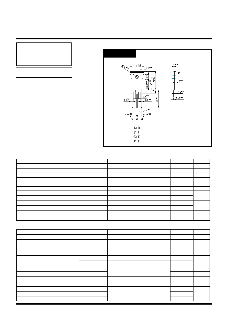
OUTLINE DIMENSIONS
Unit : mm
Case : MTO-3P
Absolute Maximum Ratings
Item
Symbol
Conditions
Ratings
Unit
Storage Temperature
Tstg
-55150
Junction Temperature
Tj
150
Collector to Base Voltage
V
CBO
600
V
Collector to Emitter Voltage
V
CEO
450
V
V
CEX
V
EB
= 5V
600
Emitter to Base Voltage
V
EBO
7
V
Collector Current DC
I
C
20
A
Collector Current Peak
I
CP
40
Base Current DC
I
B
7
A
Base Current Peak
I
BP
14
Total Transistor Dissipation
P
T
Tc = 25
150
W
Mounting Torque
TOR
0.8
Nm
Electrical Characteristics (Tc=25)
Item
Symbol
Conditions
Ratings
Unit
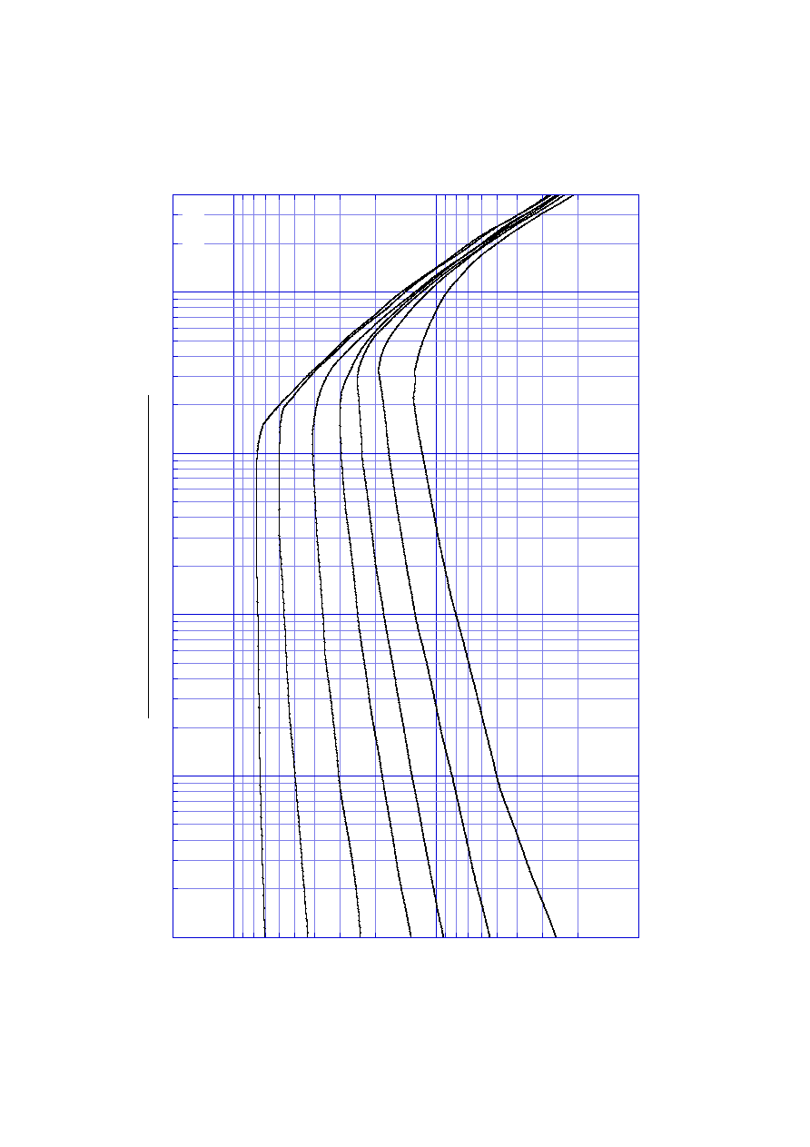
Collector to Emitter Sustaining Voltage
V
CEO
(sus)
I
C
= 0.2A
Min 450
V
Collector Cutoff Current
I
CBO
At rated Voltage
Max 0.1
mA
I
CEO
Max 0.1
Emitter Cutoff Current
I
EBO
At rated Voltage
Max 0.1
mA
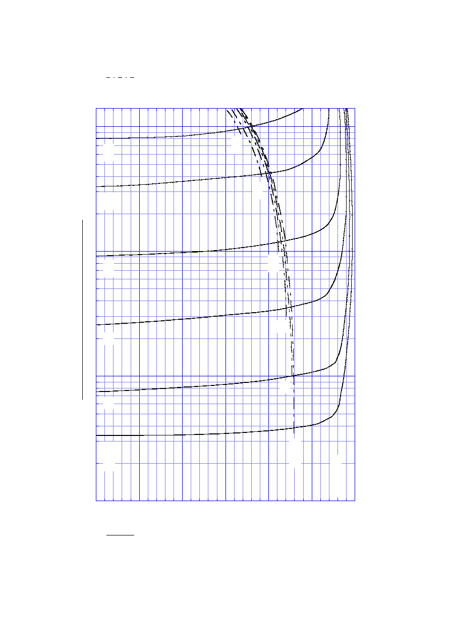
DC Current Gain
h
FE
V
CE
= 5V, I
C
= 10A
Min 10
h
FEL
V
CE
= 5V, I
C
= 1mA
Min 5
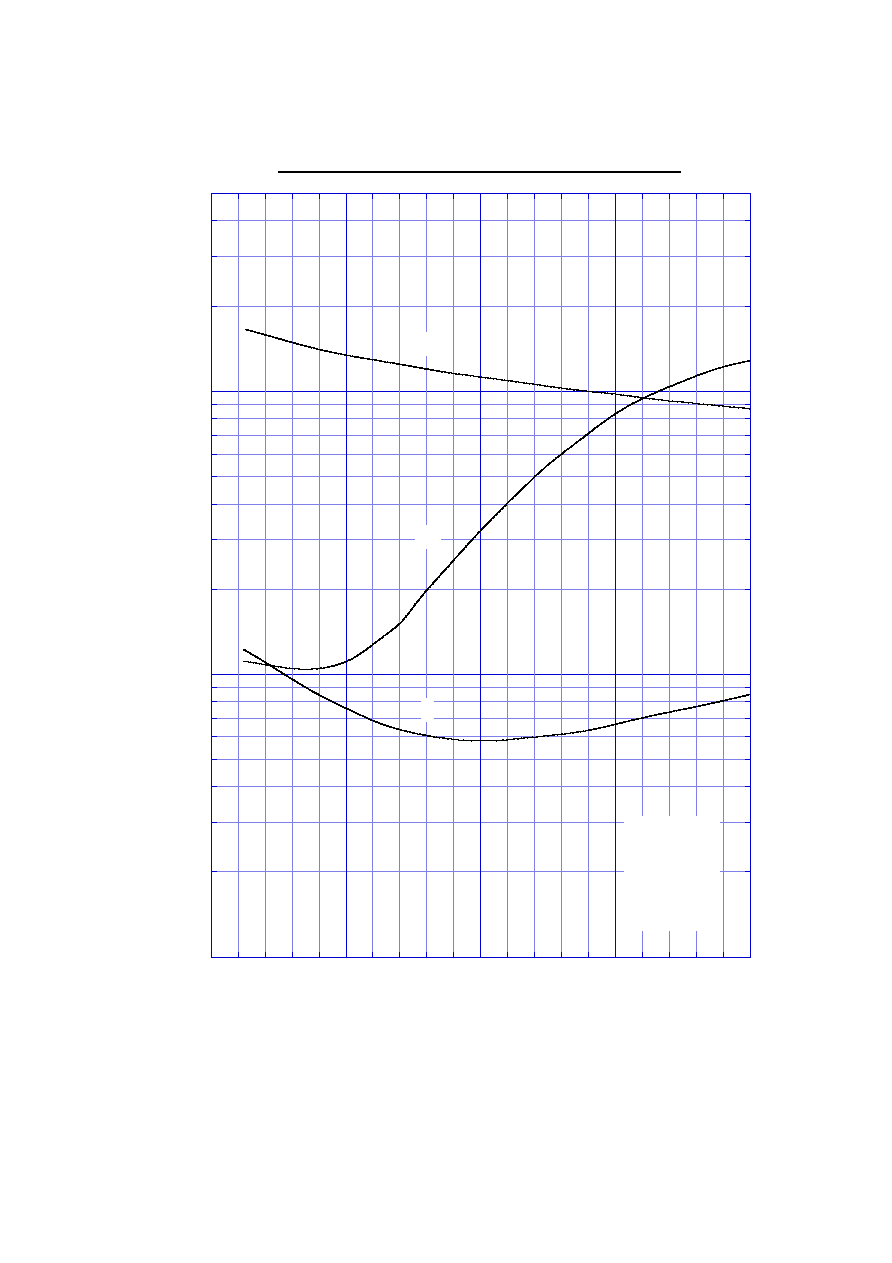
Collector to Emitter Saturation Voltage
V
CE
(sat)
I
C
= 10A
Max 1.0
V
Base to Emitter Saturation Voltage
V
BE
(sat)
I
B
= 2A
Max 1.5
V
Thermal Resistance
jc
Junction to case
Max 0.83
/W
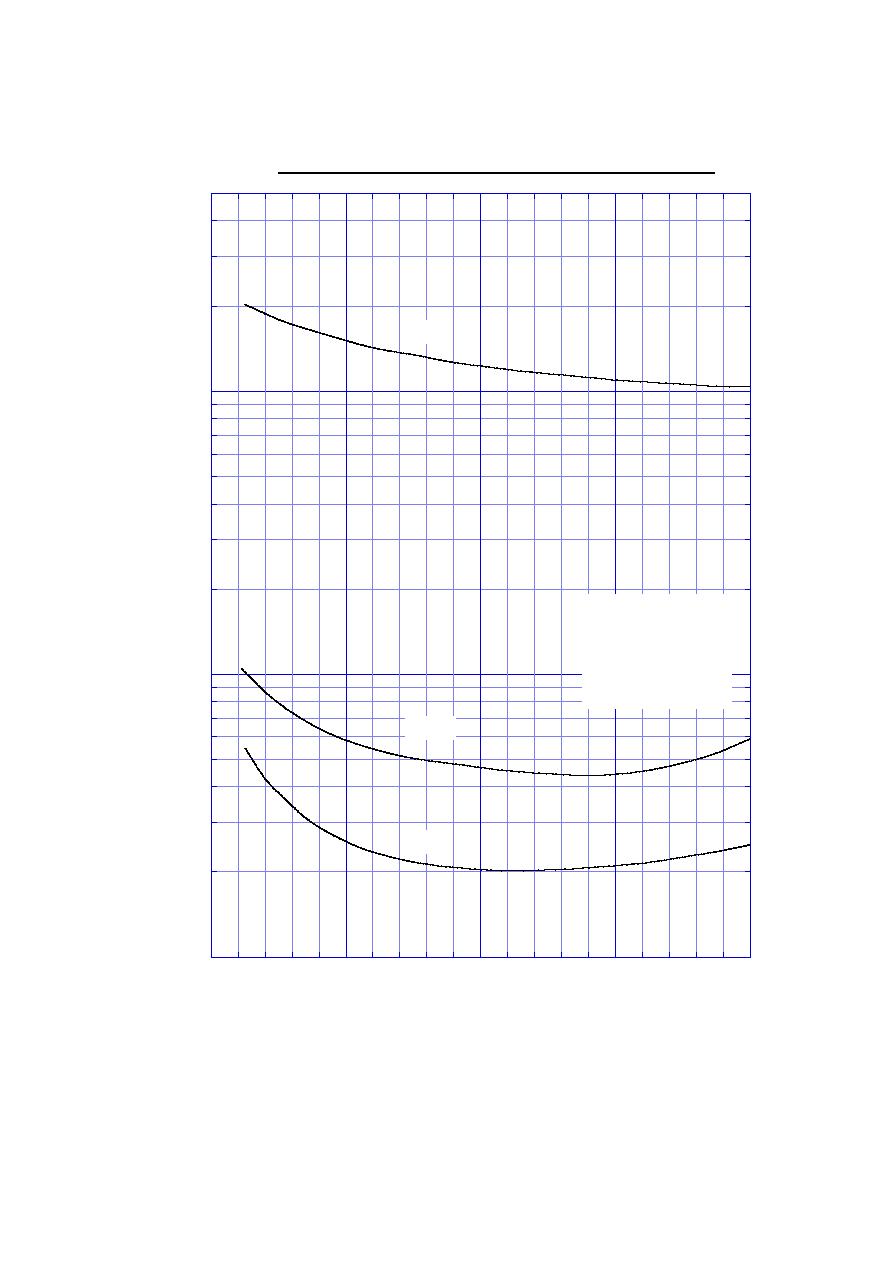
Transition Frequency
f
T
V
CE
= 10V, I
C
= 2A
STD 20
MHz
Turn on Time
ton
I
C
= 10A
Max 0.5
Storage Time
ts
I
B1
= 2A, I
B2
= 4A
Max 2.0
s
Fall Time
tf
R
L
= 15, V
BB2
= 4V
Max 0.2
FX Series
Switching Power Transistor
20A NPN
2SC4060
(T20W45FX)