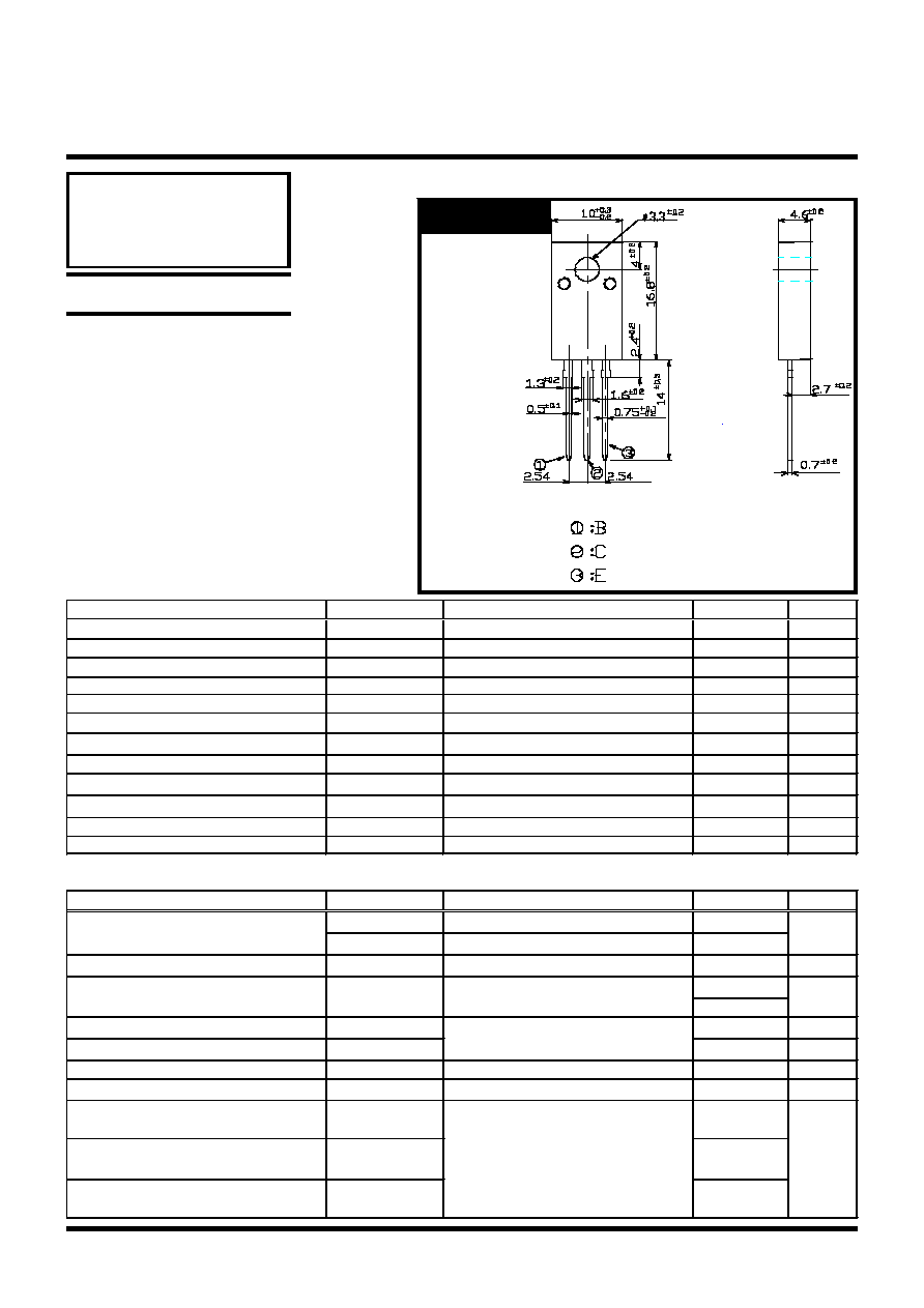
ChipFind - документация

Электронный компонент: 2SD1794

Скачать:  PDF   ZIP
Unit : mm
Copyright & Copy;2000 Shindengen Electric Mfg.Co.Ltd
RATINGS
SHINDENGEN
OUTLINE DIMENSIONS
Case : ITO-220
Darlington Transistor
10A NPN
2SD1794
(TP10L20)
Absolute Maximum Ratings
Item
Symbol
Conditions
Ratings
Unit
Storage Temperature
Tstg
-55+150
Junction Temperature
Tj
+150
Collector to Base Voltage
V
CBO
200
V
Collector to Emitter Voltage
V
CEO
200
V
Emitter to Base Voltage
V
EBO
7
V
Collector Current DC
I
C
10
A
Collector Current Peak
I
CP
15
A
Base Current DC
I
B
0.5
A
Base Current Peak
I
BP
1.0
A
Total Transistor Dissipation
P
T
Tc = 25
50
W
Dielectric Strength
Vdis
Terminals to case AC 1 minute
2
kV
Mounting Torque
TOR
(Recommended torque : 0.3Nm
0.5
Nm
Electrical Characteristics (Tc=25)
Item
Symbol
Conditions
Ratings
Unit
Collector Cutoff Current
I
CBO
V
CB
= 200V
Max 0.1
mA
I
CEO
V
CE
= 200V
Max 0.1
Emitter Cutoff Current
I
EBO
V
EB
= 7V
Max 5
mA
DC Current Gain
h
FE
V
CE
= 3V, I
C
= 5A
Min 1,500
Max 30,000
Collector to Emitter Saturation Voltage
V
CE
(sat)
IC = 5A
Max 1.5
V
Base to Emitter Saturation Voltage
V
BE
(sat)
I
B
= 10mA
Max 2.0
V
Thermal Resistance
jc
Junction to case
Max 2.5
/W
Transition Frequency
f
T
V
CE
= 10V, I
C
= 1A
TYP 20
MHz
Turn on Time
ton
Max 2
I
C
= 5A
Storage Time
ts
I
B1
= I
B2
= 10mA
Max 12
s
R
L
= 6
Fall Time
tf
V
BB2
= 4V
Max 5
100
1000
10000
100000
2SD1794
0.1
1
10
V
CE
= 3V
15
h
FE
- I
C
Tc = 150
C
100
C
50
C
25
C
0
C
-
25
C
-
55
C
Collector Current I
C
[A]
DC Current Gain h
FE
0
0.5
1
1.5
2
2.5
3
2SD1794
1
10
100
1000
0
0.5
1
1.5
2
2.5
3
0.05
0.5
0.2
20
50
5
2
200
500
2000
5000
0.02
0.05
0.5
0.2
20
5
2
0.005
0.002
I
C
= 1A
3A
5A
7A
10A
15A
Tc = 25
C
Saturation Voltage
I
C
= 1A
3A
5A
7A
10A
15A
Base Current I
B
[mA]
Collector-Emitter Voltage V
CE
[V]
Base-Emitter Voltage V
BE
[V]
0.1
1
10
0
2
4
6
8
10
2SD1794
I
B1
= 0.002I
C
I
B2
= 0.002I
C
V
BB2
= 4V
V
CC
= 50V
Tc = 25
C
t
s
t
on
t
f
Switching Time - I
C
Collector Current I
C
[A]
Switching Time t
SW
[
s]
0.1
1
10
0
50
100
150
2SD1794
I
C
= 5A
I
B1
= 10mA
I
B2
= 10mA
V
BB2
= 4V
V
CC
= 50V
t
s
t
on
t
f
Switching Time - Tc
Case Temperature Tc [
C]
Switching Time t
SW
[
s]
Transient Thermal Impedance
0.001
0.01
0.1
1
10
2SD1794
10
2
10
3
10
4
10
5
10
6
10
7
0.05
0.5
0.2
20
50
5
2
200
500
2000
5000
0.02
0.05
0.5
0.2
20
5
2
0.005
0.002
Time t [
s]
Transient Thermal Impedance
jc(t) [
C/W]
Forward Bias SOA
0.01
0.1
1
10
1
10
100
2SD1794
Tc = 25
C
Single Pulse
150
s
1ms
10ms
DC
15
200
Collector-Emitter Voltage V
CE
[V]
Collector Current I
C
[A]
P
T
limit
I
S/B
limit
0
20
40
60
80
100
0
50
100
150
2SD1794
Collector Current Derating
Collector Current Derating [%]
V
CE
= fixed
P
T
limit
I
S/B
limit
Case Temperature Tc [
C]
0
5
10
15
20
0
40
80
120
160
200
240
280
320
2SD1794
I
B1
= 0.002I
C
I
B2
= 0.004I
C
V
BB2
= 5V
Tc = 25
C
Reverse Bias SOA
Collector-Emitter Voltage V
CE
[V]
Collector Current I
C
[A]